EP0936622A2 - Dispositifs de mémoires magnétique incorporant plusieurs jonctions magnétiques de tunnel - Google Patents
Dispositifs de mémoires magnétique incorporant plusieurs jonctions magnétiques de tunnel Download PDFInfo
- Publication number
- EP0936622A2 EP0936622A2 EP99300384A EP99300384A EP0936622A2 EP 0936622 A2 EP0936622 A2 EP 0936622A2 EP 99300384 A EP99300384 A EP 99300384A EP 99300384 A EP99300384 A EP 99300384A EP 0936622 A2 EP0936622 A2 EP 0936622A2
- Authority
- EP
- European Patent Office
- Prior art keywords
- magnetic
- tunnel junctions
- region
- forming
- cell
- Prior art date
- Legal status (The legal status is an assumption and is not a legal conclusion. Google has not performed a legal analysis and makes no representation as to the accuracy of the status listed.)
- Granted
Links
- 230000005291 magnetic effect Effects 0.000 title claims abstract description 240
- 230000004044 response Effects 0.000 claims abstract description 22
- 230000005415 magnetization Effects 0.000 claims description 40
- 238000000034 method Methods 0.000 claims description 21
- 239000008187 granular material Substances 0.000 claims description 16
- 230000008878 coupling Effects 0.000 claims description 6
- 238000010168 coupling process Methods 0.000 claims description 6
- 238000005859 coupling reaction Methods 0.000 claims description 6
- 239000000696 magnetic material Substances 0.000 claims description 5
- 239000011810 insulating material Substances 0.000 claims description 4
- 238000000059 patterning Methods 0.000 claims description 2
- 210000004027 cell Anatomy 0.000 description 140
- 230000005294 ferromagnetic effect Effects 0.000 description 17
- 230000004888 barrier function Effects 0.000 description 8
- XUIMIQQOPSSXEZ-UHFFFAOYSA-N Silicon Chemical compound [Si] XUIMIQQOPSSXEZ-UHFFFAOYSA-N 0.000 description 7
- 229910052710 silicon Inorganic materials 0.000 description 7
- 239000010703 silicon Substances 0.000 description 7
- 230000008901 benefit Effects 0.000 description 5
- 239000010408 film Substances 0.000 description 5
- 238000013459 approach Methods 0.000 description 4
- 239000002800 charge carrier Substances 0.000 description 4
- 230000002950 deficient Effects 0.000 description 4
- 230000003993 interaction Effects 0.000 description 4
- 238000004519 manufacturing process Methods 0.000 description 4
- 230000010287 polarization Effects 0.000 description 4
- 239000000758 substrate Substances 0.000 description 4
- 230000008859 change Effects 0.000 description 3
- 238000000151 deposition Methods 0.000 description 3
- 230000000694 effects Effects 0.000 description 3
- 239000000463 material Substances 0.000 description 3
- 229910000889 permalloy Inorganic materials 0.000 description 3
- 238000012935 Averaging Methods 0.000 description 2
- BQCADISMDOOEFD-UHFFFAOYSA-N Silver Chemical compound [Ag] BQCADISMDOOEFD-UHFFFAOYSA-N 0.000 description 2
- 230000036755 cellular response Effects 0.000 description 2
- 230000001419 dependent effect Effects 0.000 description 2
- 230000006870 function Effects 0.000 description 2
- 230000006872 improvement Effects 0.000 description 2
- 239000002245 particle Substances 0.000 description 2
- 230000003094 perturbing effect Effects 0.000 description 2
- 229910052709 silver Inorganic materials 0.000 description 2
- 239000004332 silver Substances 0.000 description 2
- 238000003860 storage Methods 0.000 description 2
- 238000012360 testing method Methods 0.000 description 2
- 239000013598 vector Substances 0.000 description 2
- 229910020598 Co Fe Inorganic materials 0.000 description 1
- 229910002519 Co-Fe Inorganic materials 0.000 description 1
- 229910002551 Fe-Mn Inorganic materials 0.000 description 1
- 229910003271 Ni-Fe Inorganic materials 0.000 description 1
- PNEYBMLMFCGWSK-UHFFFAOYSA-N aluminium oxide Inorganic materials [O-2].[O-2].[O-2].[Al+3].[Al+3] PNEYBMLMFCGWSK-UHFFFAOYSA-N 0.000 description 1
- 238000000137 annealing Methods 0.000 description 1
- 230000005290 antiferromagnetic effect Effects 0.000 description 1
- 238000003491 array Methods 0.000 description 1
- 230000000903 blocking effect Effects 0.000 description 1
- 239000000969 carrier Substances 0.000 description 1
- 239000004020 conductor Substances 0.000 description 1
- 229910052802 copper Inorganic materials 0.000 description 1
- 230000007547 defect Effects 0.000 description 1
- 230000008021 deposition Effects 0.000 description 1
- 238000013461 design Methods 0.000 description 1
- 238000000609 electron-beam lithography Methods 0.000 description 1
- 210000004565 granule cell Anatomy 0.000 description 1
- 238000010438 heat treatment Methods 0.000 description 1
- 239000012212 insulator Substances 0.000 description 1
- 238000000025 interference lithography Methods 0.000 description 1
- 229910052742 iron Inorganic materials 0.000 description 1
- 238000001459 lithography Methods 0.000 description 1
- 239000011159 matrix material Substances 0.000 description 1
- 238000005259 measurement Methods 0.000 description 1
- 229910052697 platinum Inorganic materials 0.000 description 1
- 230000008569 process Effects 0.000 description 1
- 238000012545 processing Methods 0.000 description 1
- 230000009467 reduction Effects 0.000 description 1
- 238000004574 scanning tunneling microscopy Methods 0.000 description 1
- 238000000926 separation method Methods 0.000 description 1
- 230000003746 surface roughness Effects 0.000 description 1
- 229910052715 tantalum Inorganic materials 0.000 description 1
- 239000010409 thin film Substances 0.000 description 1
- WFKWXMTUELFFGS-UHFFFAOYSA-N tungsten Chemical compound [W] WFKWXMTUELFFGS-UHFFFAOYSA-N 0.000 description 1
- 229910052721 tungsten Inorganic materials 0.000 description 1
- 239000010937 tungsten Substances 0.000 description 1
Images


Classifications
-
- H—ELECTRICITY
- H10—SEMICONDUCTOR DEVICES; ELECTRIC SOLID-STATE DEVICES NOT OTHERWISE PROVIDED FOR
- H10B—ELECTRONIC MEMORY DEVICES
- H10B61/00—Magnetic memory devices, e.g. magnetoresistive RAM [MRAM] devices
- H10B61/10—Magnetic memory devices, e.g. magnetoresistive RAM [MRAM] devices comprising components having two electrodes, e.g. diodes or MIM elements
-
- G—PHYSICS
- G11—INFORMATION STORAGE
- G11C—STATIC STORES
- G11C5/00—Details of stores covered by group G11C11/00
- G11C5/06—Arrangements for interconnecting storage elements electrically, e.g. by wiring
- G11C5/08—Arrangements for interconnecting storage elements electrically, e.g. by wiring for interconnecting magnetic elements, e.g. toroidal cores
-
- B—PERFORMING OPERATIONS; TRANSPORTING
- B82—NANOTECHNOLOGY
- B82Y—SPECIFIC USES OR APPLICATIONS OF NANOSTRUCTURES; MEASUREMENT OR ANALYSIS OF NANOSTRUCTURES; MANUFACTURE OR TREATMENT OF NANOSTRUCTURES
- B82Y10/00—Nanotechnology for information processing, storage or transmission, e.g. quantum computing or single electron logic
-
- G—PHYSICS
- G11—INFORMATION STORAGE
- G11C—STATIC STORES
- G11C11/00—Digital stores characterised by the use of particular electric or magnetic storage elements; Storage elements therefor
- G11C11/02—Digital stores characterised by the use of particular electric or magnetic storage elements; Storage elements therefor using magnetic elements
- G11C11/14—Digital stores characterised by the use of particular electric or magnetic storage elements; Storage elements therefor using magnetic elements using thin-film elements
- G11C11/15—Digital stores characterised by the use of particular electric or magnetic storage elements; Storage elements therefor using magnetic elements using thin-film elements using multiple magnetic layers
-
- G—PHYSICS
- G11—INFORMATION STORAGE
- G11C—STATIC STORES
- G11C11/00—Digital stores characterised by the use of particular electric or magnetic storage elements; Storage elements therefor
- G11C11/02—Digital stores characterised by the use of particular electric or magnetic storage elements; Storage elements therefor using magnetic elements
- G11C11/16—Digital stores characterised by the use of particular electric or magnetic storage elements; Storage elements therefor using magnetic elements using elements in which the storage effect is based on magnetic spin effect
- G11C11/165—Auxiliary circuits
- G11C11/1659—Cell access
-
- G—PHYSICS
- G11—INFORMATION STORAGE
- G11C—STATIC STORES
- G11C11/00—Digital stores characterised by the use of particular electric or magnetic storage elements; Storage elements therefor
- G11C11/02—Digital stores characterised by the use of particular electric or magnetic storage elements; Storage elements therefor using magnetic elements
- G11C11/16—Digital stores characterised by the use of particular electric or magnetic storage elements; Storage elements therefor using magnetic elements using elements in which the storage effect is based on magnetic spin effect
- G11C11/165—Auxiliary circuits
- G11C11/1675—Writing or programming circuits or methods
-
- G—PHYSICS
- G11—INFORMATION STORAGE
- G11C—STATIC STORES
- G11C29/00—Checking stores for correct operation ; Subsequent repair; Testing stores during standby or offline operation
- G11C29/70—Masking faults in memories by using spares or by reconfiguring
- G11C29/74—Masking faults in memories by using spares or by reconfiguring using duplex memories, i.e. using dual copies
Definitions
- This application relates to magnetic devices, e.g., magnetic random access memory (“MRAM”) devices, formed from magnetic tunnel junction (“MTJ”) devices writable with magnetic stimuli.
- MRAM magnetic random access memory
- MTJ magnetic tunnel junction
- the electrical resistance of a properly formed magnetic tunnel junction memory cell depends on a magnetic writing stimulus applied to the junction.
- the cell response is hysteretic and the cell therefore retains some memory of the applied magnetic writing stimulus.
- the remnant magnetic configuration of the tunnel junction device, and its resultant electrical resistance value, is the basis for the application of such devices to electrically accessed MRAM arrays.
- each cell in an MRAM array, cells are positioned at the intersections of an exemplary rectangular grid of electrically conductive lines 1-6.
- the lines are arranged over a substrate and cross, thereby forming intersecting regions at which the cells are positioned, e.g., cell 9.
- each cell normally comprises a free magnetic region 24 and a reference magnetic region 22.
- the term reference region is used broadly herein to denote any type of region which, in cooperation with the free or changeable region, results in a detectable state of the device as a whole.
- Rotating the magnetization in the free region into one of two (possible more) selectable directions in a bi-stable manner results in binary state stored in the cell. If the cell is oriented with its magnetic easy-axis ("EA") horizontal then an electrical writing current flowing through a vertical line will apply an EA magnetic field, and a current flowing through a horizontal line will apply a hard-axis ("HA”) magnetic field, to the cell.
- EA magnetic easy-axis
- HA hard-axis
- the writing of individual cells adheres to a concept referred to as the "asteroid" for switching.
- the switching threshold of a single free region depends on the combination of EA and HA magnetic fields applied thereto.
- This "Stoner-Wohlfarth" asteroid model shown in Fig. 2a , illustrates these threshold values in the plane of applied EA and HA fields. Switching occurs when a combination of EA and HA fields at the cell results in a vector outside of the asteroid. Vectors inside the asteroid will not switch the cell from one of its current bi-stable states.
- This asteroid model also illustrates how the EA field needed to switch a device is reduced in the presence of an HA bias field.
- Selectively switching a single cell within the array is achieved by applying electrical currents through a selected pair of horizontal and vertical lines. These currents generate a combination of EA and HA fields only at the cell located at the intersection of these lines, theoretically switching the selected cell, but not the neighbouring cells.
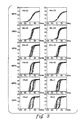
- Fig. 3 illustrates the variability in the magnetic response for 12 neighbouring MRAM devices, actually measured by the instant inventors, taking 2 EA writing loops for each device, for different HA bias fields (Hh).
- Hh HA bias fields
- Each plot shows the measured resistance change, in percent, versus the applied EA field, for each given HA bias field (He).
- He HA bias field
- a magnetic device operable using at least one electrode, comprising: at least two magnetic tunnel junctions, writable together into an average state, according to magnetic stimuli applied thereto via said at least one electrode.
- a method for storing an average state in a magnetic device using at least one electrode comprising: using at least two magnetic tunnel junctions, writable together into said state, according to magnetic stimuli applied thereto via said at least one electrode.
- the present invention relates to a magnetic device, e.g., memory cell, operable using at least one electrode, and comprising at least two magnetic tunnel junctions, writable together into an average state, according to magnetic stimuli applied thereto via the first and second electrodes.
- a magnetic device e.g., memory cell
- operable using at least one electrode and comprising at least two magnetic tunnel junctions, writable together into an average state, according to magnetic stimuli applied thereto via the first and second electrodes.
- This device may be used as a magnetic memory cell in a memory array, which includes respective pluralities of crossing first and second conductive lines forming a plurality of intersecting regions across the array.
- a plurality of magnetic memory cells, each disposed at a respective one of the plurality of intersecting regions is provided, and each cell has at least two magnetic tunnel junctions therein.
- the predictable, average response provided by the at least two magnetic tunnel junctions in each cell results in the characteristic that only the cell at an intersecting region selected by a magnetic stimuli applied via the first and second conductive lines forming the selected intersecting region is written, and other cells along the first and second conductive lines forming the selected intersecting region are not written.
- the at least two magnetic tunnel junctions may be arranged between first and second electrodes in series, or, alternatively, in parallel to accept the magnetic stimuli.
- Each of the at least two magnetic tunnel junctions may include a first region having a reference direction of magnetization, and a second, free region having a direction of magnetization changeable according to the magnetic stimuli.
- the first, reference region of each of the at least two magnetic tunnel junctions may be part of a single, cohesive magnetic region having the reference direction of magnetization.
- the second, free region of each of the at least two magnetic tunnel junctions may comprise a magnetic granule, possibly disposed in a region patterned out of a magnetic media type material, having multiple magnetic granules therein, each magnetic granule therefore forming a respective second region.
- each of the at least two magnetic tunnel junctions may comprise anti-parallel directions of magnetization therein together changeable according to the electrical and resultant magnetic stimuli applied thereto, one of the anti-parallel directions of magnetization effecting cell tunnelling in connection with its respective first region, the anti-parallel directions of magnetization providing the further characteristic of minimizing the mutual magnetic coupling with other magnetic tunnel junctions in the magnetic memory cell.
- the multiple magnetic tunnel junctions per device disclosed herein provide the advantage for a magnetic memory that memory cell selectivity can be provided on an array-wide basis using a defined operating window of magnetic stimuli applied via the bit lines and word lines. Further, since each cell is formed from multiple tunnel junctions, when the average response of the tunnel junctions in each cell is used, operation of the array is not significantly impacted by a small number of defective tunnel junctions.
- the present inventors have discovered that by averaging the magnetic response data over multiple tunnel junctions, a better and more predictable magnetic response can be obtained. For example, averaging the scattered data of Fig. 4 results in the somewhat more predictable asteroid shape of Fig. 5 .
- the present inventors then implemented, and measured the response of, eight (8) magnetic tunnel junctions arranged in parallel as one memory cell, and measured the response of four (4) such multiple-junction cells with similar junctions, but located far from each other, in the same array. The results of these measurements are shown in Fig 6. The observed scatter is due to increasing to 20 the number of loops taken. The 20-loop asteroid data of these multiple-junction cells (Fig.
- a plurality of magnetic tunnel junctions is employed in a single magnetic device, e.g., a memory cell of an MRAM array.
- the single magnetic tunnel junction ("MTJ") cell 9 of Figs. 1a-b is therefore improved by providing multiple tunnel junctions therein.
- Alternate embodiments of the multiple MTJ cell of the present invention are discussed below with reference to Figs. 9 to 14, however, by way of further introduction, the array of Figs. 1a-b is now discussed in greater detail, and in accordance with the above-incorporated, commonly assigned U.S. Patents.
- an exemplary MRAM array includes a set of electrically conductive lines that function as parallel word lines 1, 2, and 3 in a horizontal plane, and a set of electrically conductive lines that function as parallel bit lines 4, 5, and 6 in another horizontal plane.
- the bit lines are oriented in a different direction, e.g., at right angles to the word lines, so that the two sets of lines intersect when viewed from above.
- a memory cell such as typical memory cell 9 shown in detail in Fig. 1b , is located at each crossing point of the word lines and bit lines in the intersection region vertically spaced between the lines. Three word lines and three bit lines are illustrated in Fig . 1a , but the number of lines would typically be much larger.
- the memory cell 9 is arranged in a vertical stack and may include a diode 7 and a magnetic tunnel junction ("MTJ") 8.
- MTJ magnetic tunnel junction
- the vertical current path through the memory cell permits the memory cell to occupy a very small surface area.
- Contact to the word lines, the MTJ, the diode, and the contact to the bit line all occupy the same area.
- the array may be formed on a substrate, such as a silicon substrate on which there would be other circuitry.
- a layer of insulating material is usually located between the bit lines and word lines at regions of the MRAM other than the intersecting regions.
- the structure of the memory cell 9 is described in more detail with reference to Fig 1b .
- the memory cell 9 is formed on and in contact with a word line 3 ( Fig. 1a ).
- the memory cell 9 comprises a vertical stack of a diode-like device, e.g., silicon junction diode 7, and an MTJ 8 in electrical series connection.
- the diode 7 is a silicon junction diode that comprises an n-type silicon layer 10 and a p-type silicon layer 11.
- the diode's p-type silicon layer 11 is connected to the MTJ 8 via a tungsten stud 12.
- the diode's n-type silicon layer 10 is connected to word line 3.
- the MTJ 8 may be formed of a series of layers of material stacked one on top of the other.
- the MTJ 8 of Fig. 1b comprises a template layer 15, such as Pt, an initial ferromagnetic layer 16, such as permalloy (Ni-Fe), an antiferromagnetic layer (AF) 18, such as Mn-Fe, a fixed or "pinned” type of reference ferromagnetic layer (FMF) 20, such as Co, Fe or permalloy, a thin tunnelling barrier layer 22 of alumina (Al 2 O 3 ), a soft, changeable "free” ferromagnetic layer (FMS) 24, such as a sandwich of thin Co-Fe with permalloy, and a contact layer 25, such as Pt.
- a template layer 15 such as Pt
- an initial ferromagnetic layer 16 such as permalloy (Ni-Fe)
- AF antiferromagnetic layer
- FMF fixed or "pinned” type of reference ferrom
- the free layer is fabricated to have a preferred axis for the direction of magnetization called the easy axis ("EA").
- EA easy axis
- the reference layer may be fabricated to have only one preferred direction of magnetization, called its unidirectional anisotropy direction, and this direction is parallel to the easy axis of the free layer.
- the desired easy axis for the free layer is set by some combination of intrinsic anisotropy, strain-induced anisotropy and shape anisotropy of the MTJ.
- the MTJ and free layer depicted may be made in the shape of a rectangle of length L and width W, where L is larger than W ( Fig. 1b ).
- the magnetic moment of the free layer prefers to align along the direction of L.
- the unidirectional anisotropy direction of the reference layer is set by growing the Fe-Mn AF layer 18 on the initial ferromagnetic layer 16, which is itself grown on the template layer 15, such as Pt or Cu or Ta.
- the template layer 15 induces a 111 crystallographic texture in the initial ferromagnetic layer 16.
- These layers are deposited in a magnetic field directed parallel to the desired easy axis of the free layer, creating the desired intrinsic unidirectional anisotropy direction of the reference layer.
- the AF layer can be deposited on the template layer in a sufficiently large magnetic field parallel to the said easy axis while heating the substrate to a temperature higher than the blocking temperature of the AF material.
- the initial ferromagnetic layer 16 is not required. It is also possible to take advantage of the magnetostriction of the fixed layer to develop, during processing, a magnetic anisotropy which aligns magnetization along the applied magnetic field direction during deposition.
- the magnetization direction of the reference layer is more difficult to change than that of the free layer.
- the magnetization direction of the reference layer is fixed or pinned, in this embodiment.
- Shape anisotropy of the reference layer which follows the shape anisotropy of the MTJ, provides additional stability of the magnetization direction of the fixed layer.
- the magnetic fields applied to write the memory cell are large enough to reverse the direction of magnetization of the free layer, but not the direction of the reference layer. Thus, the magnetization of the fixed layer does not change direction during operation of the memory cells in the MRAM.
- the self-field of the combined current at the intersection of the write and bit lines will rotate the magnetization of the free layer of the single particular MTJ located at the intersection of the energized write and bit lines.
- the current levels are designed so that the combined self-field exceeds the switching field of the free layer. This self-field is designed to be much smaller than the field required to rotate the magnetization of the reference layer.
- the cell array architecture is designed so that the write currents do not pass through the MTJ itself. The memory cell is read by passing a sense current perpendicularly through the diode and MTJ from the reference layer through the tunnel junction barrier to the free layer (or vice versa).
- the resistance of the Al 2 O 3 tunnel barrier is strongly dependent on the thickness of the Al 2 O 3 layer, approximately varying exponentially with the thickness of this layer, this means that the electrical current largely flows perpendicularly through the Al 2 O 3 tunnel barrier.
- the probability of a charge carrier tunnelling across the barrier falls off strongly with increasing Al 2 O 3 thickness so the only carriers that tunnel across the junction are those which traverse perpendicular to the junction layer.
- the state of the memory cell is determined by measuring the resistance of the memory cell when a sense current, much smaller than the write currents, is passed perpendicularly through the MTJ. The self-field of this sense or read current is negligible and does not affect the magnetic state of the memory cell.
- the probability of tunnelling of charge carriers across the tunnel barrier depends on the relative alignment of the magnetic moments of the free and the reference layers.
- the tunnelling current is spin polarized, which means that the electrical current passing from one of the ferromagnetic layers, for example, the fixed layer, is predominantly composed of electrons of one spin type (spin up or spin down, depending on the orientation of the magnetization of the ferromagnetic layer).
- the degree of spin polarization of the current is determined by the electronic band structure of the magnetic material comprising the ferromagnetic layer at the interface of the ferromagnetic layer with the tunnel barrier.
- the first ferromagnetic layer tunnel barrier thus acts as a spin filter.
- the probability of tunnelling of the charge carriers depends on the availability of electronic states of the same spin polarization as the spin polarization of the electrical current in the second it ferromagnetic layer.
- the magnetic moment of the second ferromagnetic layer is aligned to the magnetic moment of the first ferromagnetic layer, there are more available electronic states than when the magnetic moment of the second ferromagnetic layer is aligned anti-aligned to that of the first ferromagnetic layer.
- the tunnelling probability of the charge carriers is highest when the magnetic moments of both layers are aligned, and is lowest when the magnetic moments are anti-aligned.
- the tunnelling probability takes an intermediate value.
- the electrical resistance of the cell depends on both the spin polarization of the electrical current and the electronic states in both of the ferromagnetic layers.
- the two possible magnetization directions of the free layer uniquely define two possible bit states (0 or 1) of the memory cell.
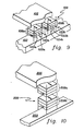
- a magnetic memory cell 109 is provided between conductive lines 103 and 105 (alternatively referred to herein as electrodes, the term electrode broadly defined as capable of imposing an electrical and/or magnetic stimulus) .
- Cell 109 includes at least two magnetic tunnel junctions 108a and 108b.
- the exemplary embodiment of Fig. 9 shows the magnetic tunnel junctions 108a and 108b arranged in parallel to accept the electrical and resultant magnetic stimuli applied thereto via lines 103 and 105.
- each magnetic tunnel junction may include a respective reference region 120a, 120b; a respective tunnelling region 122a, 122b; and a respective free region 124a, 124b.
- the writing of the magnetic memory cell is effected by changing the direction of magnetization in the free regions according to the electrical and resultant magnetic stimuli applied via lines 103 and 105, which is symbolically noted by the opposing arrows drawn in the free regions, relative to the single arrow in the reference region.
- the multiple junctions in each cell can be considered as holding an average state, but individual junctions may in fact be at different respective states within each cell.
- reference regions 120a and 120b, and tunnelling regions 122a and 122b could actually comprise respective portions of single, cohesive layers, whereas the free regions 124a and 124b are required to be separate, possibly separated by a magnetically insulating material, thereby effecting separate respective tunnelling operations for each of the at least two tunnel junctions in each cell.
- the regions 124a and 124b are required to be magnetically independent, e.g., exchange decoupled. Therefore, multiple tunnel junctions are effected by the presence of multiple free regions, in accordance with the present invention.
- the same techniques employed to form the magnetic memory cells in the above-incorporated, commonly assigned U.S. Patents can be used to form the multiple tunnel junction cells of the present invention.
- the multiple tunnel junctions in each cell can be patterned using e-beam lithography, interference lithography, STM lithography, or stamping into resist, or other known techniques to define small devices.
- magnetic memory cell 209 includes separate tunnel junctions 208a and 208b arranged in series between lines 203 and 205 to accept the electrical and resultant magnetic stimuli.
- This magnetic memory cell structure can be formed in accordance with the techniques described in the above-incorporated commonly assigned U.S. Patents, by adding additional layers to define the additional magnetic tunnel junctions within each cell.
- a magnetic memory cell 309 having multiple magnetic tunnel junctions 308a-h therein, each having mutually magnetically decoupled free regions 324a-h (not all of which are designated, for clarity), and including a single tunnelling layer 322.
- an exemplary underlying reference region 320 is shown comprising a single, cohesive magnetically pinned layer.
- the multiple, decoupled magnetic "granules" forming the single magnetic memory cell can be formed by, for example, depositing magnetic granules on top of an insulator, and then embedding them in a non-magnetic matrix, co-deposition of insulating and conducting materials, or isolating grains.
- the free layers of the devices are deposited in the form of a succession of at least two thin layers: alternating magnetic material and non-magnetic material (such as silver).
- alternating magnetic material such as silver
- non-magnetic material such as silver
- each magnetic granule could be formed as a sphere having an encircling tunnel junction layer, which together are thereafter deposited over the pinned layer.
- Fig. 12 illustrates another potential fabrication technique for the granule approach of Fig. 11 , wherein cell regions, e.g., cell region 409 having granules 408a-e therein, are patterned from a layer 424 resembling a planar magnetic media.
- magnetic media layer 424 can be deposited, and thereafter patterned, thereby forming the cell regions, e.g., 409, each having multiple magnetic granules therein.
- memory cells based on tunnel junction devices typically used a continuous metallic film. Although these films are often polycrystalline, the magnetization in the grains is strongly exchanged coupled so that, magnetically, each cell acts as a continuous film and a single junction device.
- the present invention is directed to the use of a granular film similar to that used in magnetic recording as thin film media. These films are made with grains that are magnetically decoupled from an exchange interaction point of view. The grains are not exchanged coupled although they will have some magnetostatic interaction.
- each particle or grain is a separate junction. As each particle is different and located differently, each junction will switch at a slightly different coercive filed. When operating the memory cell, it is not necessary to switch all the junctions in the selected cell but just to switch a majority of them so that the written state can be detected during read. Similarly, it is not necessary to not switch all the junctions in a non-selected cell, just to leave the majority of junctions unperturbed so that the storage state is not modified.
- multiple exchange-decoupled grains in memory cells allow for a tradeoff between signal amplitude and reproducibility in the switching threshold.
- the underlying reference region 420 and tunnelling region 422 in this type of cell can comprise single, cohesive layers. Further, as discussed above, the overlying and underlying crossing conductive lines 402, 403, 405 and 406 are provided for writing and reading each cell region.
- each tunnel junction includes a respective pinned region e.g., 520a, a respective tunnelling region, e.g., 522a, and a respective anti-parallel free region, e.g., 524a, comprising two regions having changeable, but opposing directions of magnetization therein.
- the bottom region of magnetization in region 524a effects tunnelling in connection with the pinned layer 520a, through tunnelling layer 522a.
- magnetic tunnel junction 508a reduces any field coupling to the adjacent tunnel junctions 508b and 508c.
- free regions (and/or the pinned or reference region) in each tunnel junction reduces the field coupling between the tunnel junctions, and thus ensures magnetic independence thereof.
- the anti-parallel regions can be implemented according to the principles of commonly assigned U.S. Patent 5,341,118, incorporated herein by reference in its entirety.
- magnetic memory cell 609 is provided and includes six tunnel junctions 608a-f between word line 603 and bit line 605.
- the tunnel junctions are designed to be longer than the width of line 605, so that the more stable magnetic properties toward the middle of the elongated free regions are relied upon for cell operation, rather than the more magnetically unstable end portions thereof.
- This concept is developed in greater detail in the above-incorporated U.S. Patent Application, "LIMITING MAGNETIC WRITING FIELDS TO A PREFERRED PORTION OF A CHANGEABLE MAGNETIC REGION IN MAGNETIC DEVICES.”
- the present invention by providing multiple magnetic tunnel junctions in each magnetic memory cell, increases the predictability of the response of each respective cell, and thus provides cell selectivity on an array-wide basis.
- the cell selectivity is improved because the average response of each cell can be predicted such that an operating window of applied electrical and therefore magnetic stimuli can be used.
- a set of applied easy axis and hard axis fields can therefore be identified that switches cells if applied together, but that would not switch cells if either is applied separately, i.e., cells along either the asserted bitline or wordline other than the cell at the intersection of the asserted bitline and wordline.
- Another feature/advantage of the present invention is that by providing multiple magnetic tunnel junctions in each cell, there is a built-in tolerance for defective junctions.
- a defective junction for example, one with no response to the applied electric/magnetic stimuli, will not affect the overall performance of the array since it is the average response over many junctions that effects the storage of the state in each cell.
- a defective tunnel junction will completely eliminate the ability to store data in a given cell, and therefore defeat the operation of the entire array.
- multiple junction cell 709 may include junctions 708a-j therein arranged with the spacing and layout shown, at a microscopic, micromagnetic level.
- the macroscopic, macromagnetic stimulus field shape 710 results from this spacing and layout, and can therefore be customized as required in accordance with particular system requirements.
Landscapes
- Engineering & Computer Science (AREA)
- Computer Hardware Design (AREA)
- Chemical & Material Sciences (AREA)
- Nanotechnology (AREA)
- Physics & Mathematics (AREA)
- Mathematical Physics (AREA)
- Theoretical Computer Science (AREA)
- Crystallography & Structural Chemistry (AREA)
- Hall/Mr Elements (AREA)
- Semiconductor Memories (AREA)
- Mram Or Spin Memory Techniques (AREA)
Applications Claiming Priority (2)
| Application Number | Priority Date | Filing Date | Title |
|---|---|---|---|
| US09/021,342 US6072718A (en) | 1998-02-10 | 1998-02-10 | Magnetic memory devices having multiple magnetic tunnel junctions therein |
| US21342 | 1998-02-10 |
Publications (3)
| Publication Number | Publication Date |
|---|---|
| EP0936622A2 true EP0936622A2 (fr) | 1999-08-18 |
| EP0936622A3 EP0936622A3 (fr) | 2000-11-08 |
| EP0936622B1 EP0936622B1 (fr) | 2002-10-02 |
Family
ID=21803670
Family Applications (1)
| Application Number | Title | Priority Date | Filing Date |
|---|---|---|---|
| EP99300384A Expired - Lifetime EP0936622B1 (fr) | 1998-02-10 | 1999-01-20 | Dispositifs de mémoires magnétique incorporant plusieurs jonctions magnétiques de tunnel |
Country Status (5)
| Country | Link |
|---|---|
| US (1) | US6072718A (fr) |
| EP (1) | EP0936622B1 (fr) |
| JP (1) | JP3443026B2 (fr) |
| KR (1) | KR100339176B1 (fr) |
| DE (1) | DE69903206T2 (fr) |
Cited By (4)
| Publication number | Priority date | Publication date | Assignee | Title |
|---|---|---|---|---|
| EP1134743A3 (fr) * | 2000-03-13 | 2002-04-10 | Matsushita Electric Industrial Co., Ltd. | Dispositif magnéto-résistif et dispositif de mémoire d'un type à effet magnéto-résistif |
| WO2002099905A1 (fr) * | 2001-05-31 | 2002-12-12 | National Institute Of Advanced Industrial Science And Technology | Element de magnetoresistance tunnel |
| US6885049B2 (en) * | 2000-02-28 | 2005-04-26 | Hewlett-Packard Development Company, L.P. | Spin dependent tunneling junctions including ferromagnetic layers having flattened peaks |
| EP1151482A4 (fr) * | 1999-01-06 | 2010-02-17 | Nve Corp | Capteur a effet tunnel dependant du spin |
Families Citing this family (131)
| Publication number | Priority date | Publication date | Assignee | Title |
|---|---|---|---|---|
| US20040017721A1 (en) * | 1998-10-30 | 2004-01-29 | Schwabe Nikolai Franz Gregoe | Magnetic storage device |
| JP4560847B2 (ja) * | 1998-12-28 | 2010-10-13 | ヤマハ株式会社 | 磁気抵抗ランダムアクセスメモリ |
| EP1141960B1 (fr) * | 1999-01-13 | 2002-07-03 | Infineon Technologies AG | Architecture d'ecriture/lecture pour ram magnetoresistive |
| DE50000924D1 (de) * | 1999-03-19 | 2003-01-23 | Infineon Technologies Ag | Speicherzellenanordnung und verfahren zu deren herstellung |
| US6381171B1 (en) * | 1999-05-19 | 2002-04-30 | Kabushiki Kaisha Toshiba | Magnetic element, magnetic read head, magnetic storage device, magnetic memory device |
| US6611405B1 (en) * | 1999-09-16 | 2003-08-26 | Kabushiki Kaisha Toshiba | Magnetoresistive element and magnetic memory device |
| WO2001067459A1 (fr) * | 2000-03-09 | 2001-09-13 | Lienau Richard M | Procede et appareil de lecture de donnees a partir d'une cellule de memoire ferromagnetique |
| US6269018B1 (en) * | 2000-04-13 | 2001-07-31 | International Business Machines Corporation | Magnetic random access memory using current through MTJ write mechanism |
| JP4309075B2 (ja) * | 2000-07-27 | 2009-08-05 | 株式会社東芝 | 磁気記憶装置 |
| JP4020573B2 (ja) | 2000-07-27 | 2007-12-12 | 富士通株式会社 | 磁性メモリデバイス、および磁性メモリデバイスにおけるデータ読み出し方法 |
| JP4149647B2 (ja) | 2000-09-28 | 2008-09-10 | 株式会社東芝 | 半導体記憶装置及びその製造方法 |
| US6724674B2 (en) * | 2000-11-08 | 2004-04-20 | International Business Machines Corporation | Memory storage device with heating element |
| US6563743B2 (en) * | 2000-11-27 | 2003-05-13 | Hitachi, Ltd. | Semiconductor device having dummy cells and semiconductor device having dummy cells for redundancy |
| US6611453B2 (en) * | 2001-01-24 | 2003-08-26 | Infineon Technologies Ag | Self-aligned cross-point MRAM device with aluminum metallization layers |
| US6567297B2 (en) * | 2001-02-01 | 2003-05-20 | Micron Technology, Inc. | Method and apparatus for sensing resistance values of memory cells |
| US6515341B2 (en) * | 2001-02-26 | 2003-02-04 | Motorola, Inc. | Magnetoelectronics element having a stressed over-layer configured for alteration of the switching energy barrier |
| JP4731041B2 (ja) * | 2001-05-16 | 2011-07-20 | ルネサスエレクトロニクス株式会社 | 薄膜磁性体記憶装置 |
| JP3807254B2 (ja) * | 2001-05-30 | 2006-08-09 | ソニー株式会社 | 磁気抵抗効果素子、磁気抵抗効果型磁気センサ、および磁気抵抗効果型磁気ヘッド |
| US6756620B2 (en) * | 2001-06-29 | 2004-06-29 | Intel Corporation | Low-voltage and interface damage-free polymer memory device |
| US6858862B2 (en) * | 2001-06-29 | 2005-02-22 | Intel Corporation | Discrete polymer memory array and method of making same |
| US6960479B2 (en) * | 2001-07-20 | 2005-11-01 | Intel Corporation | Stacked ferroelectric memory device and method of making same |
| US6624457B2 (en) | 2001-07-20 | 2003-09-23 | Intel Corporation | Stepped structure for a multi-rank, stacked polymer memory device and method of making same |
| US7566478B2 (en) | 2001-07-25 | 2009-07-28 | Nantero, Inc. | Methods of making carbon nanotube films, layers, fabrics, ribbons, elements and articles |
| US6574130B2 (en) * | 2001-07-25 | 2003-06-03 | Nantero, Inc. | Hybrid circuit having nanotube electromechanical memory |
| US6911682B2 (en) | 2001-12-28 | 2005-06-28 | Nantero, Inc. | Electromechanical three-trace junction devices |
| US6835591B2 (en) * | 2001-07-25 | 2004-12-28 | Nantero, Inc. | Methods of nanotube films and articles |
| US7259410B2 (en) | 2001-07-25 | 2007-08-21 | Nantero, Inc. | Devices having horizontally-disposed nanofabric articles and methods of making the same |
| US6706402B2 (en) | 2001-07-25 | 2004-03-16 | Nantero, Inc. | Nanotube films and articles |
| US6919592B2 (en) | 2001-07-25 | 2005-07-19 | Nantero, Inc. | Electromechanical memory array using nanotube ribbons and method for making same |
| US6643165B2 (en) | 2001-07-25 | 2003-11-04 | Nantero, Inc. | Electromechanical memory having cell selection circuitry constructed with nanotube technology |
| US6924538B2 (en) | 2001-07-25 | 2005-08-02 | Nantero, Inc. | Devices having vertically-disposed nanofabric articles and methods of making the same |
| US6869855B1 (en) | 2001-09-02 | 2005-03-22 | Borealis Technical Limited | Method for making electrode pairs |
| US6795281B2 (en) * | 2001-09-25 | 2004-09-21 | Hewlett-Packard Development Company, L.P. | Magneto-resistive device including soft synthetic ferrimagnet reference layer |
| KR100402390B1 (ko) * | 2001-10-05 | 2003-10-17 | 삼성전자주식회사 | 다층 터널접합층을 갖는 반도체 기억장치 및 그 제조방법 |
| US6545906B1 (en) | 2001-10-16 | 2003-04-08 | Motorola, Inc. | Method of writing to scalable magnetoresistance random access memory element |
| KR20030034500A (ko) * | 2001-10-23 | 2003-05-09 | 주식회사 하이닉스반도체 | 마그네틱 램 |
| US6570783B1 (en) * | 2001-11-15 | 2003-05-27 | Micron Technology, Inc. | Asymmetric MRAM cell and bit design for improving bit yield |
| JP3866567B2 (ja) * | 2001-12-13 | 2007-01-10 | 株式会社東芝 | 半導体記憶装置及びその製造方法 |
| JP4278325B2 (ja) | 2001-12-19 | 2009-06-10 | 株式会社ルネサステクノロジ | 半導体集積回路装置 |
| US6795334B2 (en) * | 2001-12-21 | 2004-09-21 | Kabushiki Kaisha Toshiba | Magnetic random access memory |
| KR100457159B1 (ko) * | 2001-12-26 | 2004-11-16 | 주식회사 하이닉스반도체 | 마그네틱 램 |
| KR100465598B1 (ko) * | 2001-12-26 | 2005-01-13 | 주식회사 하이닉스반도체 | 쇼트키 다이오드를 이용한 마그네틱 램 |
| JP2003197875A (ja) * | 2001-12-28 | 2003-07-11 | Toshiba Corp | 磁気記憶装置 |
| US6784028B2 (en) | 2001-12-28 | 2004-08-31 | Nantero, Inc. | Methods of making electromechanical three-trace junction devices |
| US7176505B2 (en) | 2001-12-28 | 2007-02-13 | Nantero, Inc. | Electromechanical three-trace junction devices |
| US6625059B1 (en) * | 2002-03-06 | 2003-09-23 | Hewlett-Packard Development Company, L.P. | Synthetic ferrimagnet reference layer for a magnetic storage device |
| US7335395B2 (en) | 2002-04-23 | 2008-02-26 | Nantero, Inc. | Methods of using pre-formed nanotubes to make carbon nanotube films, layers, fabrics, ribbons, elements and articles |
| US6667897B1 (en) | 2002-06-28 | 2003-12-23 | International Business Machines Corporation | Magnetic tunnel junction containing a ferrimagnetic layer and anti-parallel layer |
| US7095646B2 (en) | 2002-07-17 | 2006-08-22 | Freescale Semiconductor, Inc. | Multi-state magnetoresistance random access cell with improved memory storage density |
| JP2004111437A (ja) * | 2002-09-13 | 2004-04-08 | Toshiba Corp | 磁気記憶装置 |
| US6744651B2 (en) * | 2002-09-20 | 2004-06-01 | Taiwan Semiconductor Manufacturing Company | Local thermal enhancement of magnetic memory cell during programming |
| US6639830B1 (en) | 2002-10-22 | 2003-10-28 | Btg International Ltd. | Magnetic memory device |
| US6775183B2 (en) * | 2002-10-22 | 2004-08-10 | Btg International Ltd. | Magnetic memory device employing giant magnetoresistance effect |
| US6890767B2 (en) * | 2002-10-24 | 2005-05-10 | Taiwan Semiconductor Manufacturing Company, Ltd. | Method to reduce switch threshold of soft magnetic films |
| US6660568B1 (en) | 2002-11-07 | 2003-12-09 | International Business Machines Corporation | BiLevel metallization for embedded back end of the line structures |
| US7023723B2 (en) * | 2002-11-12 | 2006-04-04 | Nve Corporation | Magnetic memory layers thermal pulse transitions |
| US7560136B2 (en) | 2003-01-13 | 2009-07-14 | Nantero, Inc. | Methods of using thin metal layers to make carbon nanotube films, layers, fabrics, ribbons, elements and articles |
| US6909628B2 (en) * | 2003-02-13 | 2005-06-21 | Taiwan Semiconductor Manufacturing Company, Ltd. | High density magnetic RAM and array architecture using a one transistor, one diode, and one MTJ cell |
| JP2004288311A (ja) * | 2003-03-24 | 2004-10-14 | Toshiba Corp | 半導体記憶装置及びその制御方法 |
| US7230804B2 (en) * | 2003-05-02 | 2007-06-12 | Hitachi Global Storage Technologies Netherlands B.V. | Method and apparatus for providing a magnetic tunnel transistor with a self-pinned emitter |
| US7916435B1 (en) | 2003-05-02 | 2011-03-29 | Hitachi Global Storage Technologies Netherlands B.V. | Magnetic tunnel transistor having a base structure that provides polarization of unpolarized electrons from an emitter based upon a magnetic orientation of a free layer and a self-pinned layer |
| US6956763B2 (en) | 2003-06-27 | 2005-10-18 | Freescale Semiconductor, Inc. | MRAM element and methods for writing the MRAM element |
| JP4142993B2 (ja) * | 2003-07-23 | 2008-09-03 | 株式会社東芝 | 磁気メモリ装置の製造方法 |
| JP4534441B2 (ja) * | 2003-07-25 | 2010-09-01 | Tdk株式会社 | 磁気記憶セル及びこれを用いた磁気メモリデバイス |
| US6967366B2 (en) | 2003-08-25 | 2005-11-22 | Freescale Semiconductor, Inc. | Magnetoresistive random access memory with reduced switching field variation |
| US7536612B2 (en) * | 2003-08-29 | 2009-05-19 | International Business Machines Corporation | Field spike monitor for MRAM |
| US20050073878A1 (en) * | 2003-10-03 | 2005-04-07 | Taiwan Semiconductor Manufacturing Co., Ltd. | Multi-sensing level MRAM structure with different magnetoresistance ratios |
| US7611911B2 (en) * | 2003-10-08 | 2009-11-03 | International Business Machines Corporation | Method and system for patterning of magnetic thin films using gaseous transformation to transform a magnetic portion to a non-magnetic portion |
| US20060281258A1 (en) * | 2004-10-06 | 2006-12-14 | Bernard Dieny | Magnetic tunnel junction device and writing/reading method for said device |
| FR2860910B1 (fr) * | 2003-10-10 | 2006-02-10 | Commissariat Energie Atomique | Dispositif a jonction tunnel magnetique et procede d'ecriture/lecture d'un tel dispositif |
| US20050105328A1 (en) * | 2003-11-17 | 2005-05-19 | Ho Chiahua | Perpendicular MRAM with high magnetic transition and low programming current |
| US6925000B2 (en) | 2003-12-12 | 2005-08-02 | Maglabs, Inc. | Method and apparatus for a high density magnetic random access memory (MRAM) with stackable architecture |
| US7102920B2 (en) * | 2004-03-23 | 2006-09-05 | Hewlett-Packard Development Company, L.P. | Soft-reference three conductor magnetic memory storage device |
| US7211446B2 (en) * | 2004-06-11 | 2007-05-01 | International Business Machines Corporation | Method of patterning a magnetic tunnel junction stack for a magneto-resistive random access memory |
| US7061037B2 (en) * | 2004-07-06 | 2006-06-13 | Maglabs, Inc. | Magnetic random access memory with multiple memory layers and improved memory cell selectivity |
| US7072208B2 (en) * | 2004-07-28 | 2006-07-04 | Headway Technologies, Inc. | Vortex magnetic random access memory |
| US7092284B2 (en) * | 2004-08-20 | 2006-08-15 | Infineon Technologies Ag | MRAM with magnetic via for storage of information and field sensor |
| US7075818B2 (en) * | 2004-08-23 | 2006-07-11 | Maglabs, Inc. | Magnetic random access memory with stacked memory layers having access lines for writing and reading |
| US7129098B2 (en) | 2004-11-24 | 2006-10-31 | Freescale Semiconductor, Inc. | Reduced power magnetoresistive random access memory elements |
| US7088611B2 (en) * | 2004-11-30 | 2006-08-08 | Infineon Technologies Ag | MRAM with switchable ferromagnetic offset layer |
| US7061797B1 (en) * | 2004-12-30 | 2006-06-13 | Infineon Technologies Ag | Hybrid memory cell for spin-polarized electron current induced switching and writing/reading process using such memory cell |
| JP4373938B2 (ja) * | 2005-02-17 | 2009-11-25 | 株式会社東芝 | 磁気ランダムアクセスメモリ |
| US7635903B2 (en) * | 2005-09-13 | 2009-12-22 | Everspin Technologies, Inc. | Oscillator and method of manufacture |
| JP2007081280A (ja) | 2005-09-16 | 2007-03-29 | Fujitsu Ltd | 磁気抵抗効果素子及び磁気メモリ装置 |
| JP4997789B2 (ja) * | 2006-02-23 | 2012-08-08 | Tdk株式会社 | 磁気メモリ |
| US8084835B2 (en) * | 2006-10-20 | 2011-12-27 | Avalanche Technology, Inc. | Non-uniform switching based non-volatile magnetic based memory |
| US20070253245A1 (en) * | 2006-04-27 | 2007-11-01 | Yadav Technology | High Capacity Low Cost Multi-Stacked Cross-Line Magnetic Memory |
| US8535952B2 (en) * | 2006-02-25 | 2013-09-17 | Avalanche Technology, Inc. | Method for manufacturing non-volatile magnetic memory |
| US20080246104A1 (en) * | 2007-02-12 | 2008-10-09 | Yadav Technology | High Capacity Low Cost Multi-State Magnetic Memory |
| US7732881B2 (en) * | 2006-11-01 | 2010-06-08 | Avalanche Technology, Inc. | Current-confined effect of magnetic nano-current-channel (NCC) for magnetic random access memory (MRAM) |
| US8508984B2 (en) * | 2006-02-25 | 2013-08-13 | Avalanche Technology, Inc. | Low resistance high-TMR magnetic tunnel junction and process for fabrication thereof |
| US8363457B2 (en) * | 2006-02-25 | 2013-01-29 | Avalanche Technology, Inc. | Magnetic memory sensing circuit |
| US8063459B2 (en) * | 2007-02-12 | 2011-11-22 | Avalanche Technologies, Inc. | Non-volatile magnetic memory element with graded layer |
| US8018011B2 (en) * | 2007-02-12 | 2011-09-13 | Avalanche Technology, Inc. | Low cost multi-state magnetic memory |
| US8058696B2 (en) * | 2006-02-25 | 2011-11-15 | Avalanche Technology, Inc. | High capacity low cost multi-state magnetic memory |
| US8183652B2 (en) * | 2007-02-12 | 2012-05-22 | Avalanche Technology, Inc. | Non-volatile magnetic memory with low switching current and high thermal stability |
| US8120949B2 (en) * | 2006-04-27 | 2012-02-21 | Avalanche Technology, Inc. | Low-cost non-volatile flash-RAM memory |
| US7508042B2 (en) * | 2006-12-22 | 2009-03-24 | Magic Technologies, Inc. | Spin transfer MRAM device with magnetic biasing |
| US7869266B2 (en) * | 2007-10-31 | 2011-01-11 | Avalanche Technology, Inc. | Low current switching magnetic tunnel junction design for magnetic memory using domain wall motion |
| US20090218645A1 (en) * | 2007-02-12 | 2009-09-03 | Yadav Technology Inc. | multi-state spin-torque transfer magnetic random access memory |
| US8542524B2 (en) * | 2007-02-12 | 2013-09-24 | Avalanche Technology, Inc. | Magnetic random access memory (MRAM) manufacturing process for a small magnetic tunnel junction (MTJ) design with a low programming current requirement |
| WO2009054182A1 (fr) | 2007-10-25 | 2009-04-30 | Fuji Electric Holdings Co., Ltd. | Élément de vanne de spin et son procédé de fabrication |
| US8004881B2 (en) * | 2007-12-19 | 2011-08-23 | Qualcomm Incorporated | Magnetic tunnel junction device with separate read and write paths |
| US7936596B2 (en) * | 2008-02-01 | 2011-05-03 | Qualcomm Incorporated | Magnetic tunnel junction cell including multiple magnetic domains |
| US8802451B2 (en) | 2008-02-29 | 2014-08-12 | Avalanche Technology Inc. | Method for manufacturing high density non-volatile magnetic memory |
| US7579197B1 (en) | 2008-03-04 | 2009-08-25 | Qualcomm Incorporated | Method of forming a magnetic tunnel junction structure |
| US8634231B2 (en) | 2009-08-24 | 2014-01-21 | Qualcomm Incorporated | Magnetic tunnel junction structure |
| US7781231B2 (en) * | 2008-03-07 | 2010-08-24 | Qualcomm Incorporated | Method of forming a magnetic tunnel junction device |
| US7885105B2 (en) * | 2008-03-25 | 2011-02-08 | Qualcomm Incorporated | Magnetic tunnel junction cell including multiple vertical magnetic domains |
| US8659852B2 (en) * | 2008-04-21 | 2014-02-25 | Seagate Technology Llc | Write-once magentic junction memory array |
| US7855911B2 (en) * | 2008-05-23 | 2010-12-21 | Seagate Technology Llc | Reconfigurable magnetic logic device using spin torque |
| US7852663B2 (en) * | 2008-05-23 | 2010-12-14 | Seagate Technology Llc | Nonvolatile programmable logic gates and adders |
| US7881098B2 (en) * | 2008-08-26 | 2011-02-01 | Seagate Technology Llc | Memory with separate read and write paths |
| US7985994B2 (en) * | 2008-09-29 | 2011-07-26 | Seagate Technology Llc | Flux-closed STRAM with electronically reflective insulative spacer |
| US8169810B2 (en) | 2008-10-08 | 2012-05-01 | Seagate Technology Llc | Magnetic memory with asymmetric energy barrier |
| US8039913B2 (en) * | 2008-10-09 | 2011-10-18 | Seagate Technology Llc | Magnetic stack with laminated layer |
| US8089132B2 (en) | 2008-10-09 | 2012-01-03 | Seagate Technology Llc | Magnetic memory with phonon glass electron crystal material |
| US20100102405A1 (en) * | 2008-10-27 | 2010-04-29 | Seagate Technology Llc | St-ram employing a spin filter |
| US8045366B2 (en) | 2008-11-05 | 2011-10-25 | Seagate Technology Llc | STRAM with composite free magnetic element |
| US8043732B2 (en) | 2008-11-11 | 2011-10-25 | Seagate Technology Llc | Memory cell with radial barrier |
| US7826181B2 (en) * | 2008-11-12 | 2010-11-02 | Seagate Technology Llc | Magnetic memory with porous non-conductive current confinement layer |
| US8289756B2 (en) | 2008-11-25 | 2012-10-16 | Seagate Technology Llc | Non volatile memory including stabilizing structures |
| US7826259B2 (en) * | 2009-01-29 | 2010-11-02 | Seagate Technology Llc | Staggered STRAM cell |
| US7999338B2 (en) | 2009-07-13 | 2011-08-16 | Seagate Technology Llc | Magnetic stack having reference layers with orthogonal magnetization orientation directions |
| US9385308B2 (en) * | 2010-03-26 | 2016-07-05 | Qualcomm Incorporated | Perpendicular magnetic tunnel junction structure |
| US8625337B2 (en) | 2010-05-06 | 2014-01-07 | Qualcomm Incorporated | Method and apparatus of probabilistic programming multi-level memory in cluster states of bi-stable elements |
| DE102010055754A1 (de) * | 2010-12-22 | 2012-06-28 | Sensitec Gmbh | Magnetoresistives Sensorelement |
| US9236561B2 (en) | 2011-09-12 | 2016-01-12 | Samsung Electronics Co., Ltd. | Method and system for providing multiple self-aligned logic cells in a single stack |
| US9548095B2 (en) * | 2014-08-20 | 2017-01-17 | Everspin Technologies, Inc. | Redundant magnetic tunnel junctions in magnetoresistive memory |
| US11386320B2 (en) | 2019-03-06 | 2022-07-12 | International Business Machines Corporation | Magnetic domain wall-based non-volatile, linear and bi-directional synaptic weight element |
| US11222920B2 (en) * | 2020-02-04 | 2022-01-11 | Western Digital Technologies, Inc. | Magnetic device including multiferroic regions and methods of forming the same |
Family Cites Families (9)
| Publication number | Priority date | Publication date | Assignee | Title |
|---|---|---|---|---|
| IT1230363B (it) * | 1989-08-01 | 1991-10-18 | Sgs Thomson Microelectronics | Cella di memoria eeprom, con protezione migliorata da errori dovuti a rottura della cella. |
| MY108176A (en) * | 1991-02-08 | 1996-08-30 | Hitachi Global Storage Tech Netherlands B V | Magnetoresistive sensor based on oscillations in the magnetoresistance |
| US5408377A (en) * | 1993-10-15 | 1995-04-18 | International Business Machines Corporation | Magnetoresistive sensor with improved ferromagnetic sensing layer and magnetic recording system using the sensor |
| JP3767930B2 (ja) * | 1995-11-13 | 2006-04-19 | 沖電気工業株式会社 | 情報の記録・再生方法および情報記憶装置 |
| US5659499A (en) * | 1995-11-24 | 1997-08-19 | Motorola | Magnetic memory and method therefor |
| US5650958A (en) * | 1996-03-18 | 1997-07-22 | International Business Machines Corporation | Magnetic tunnel junctions with controlled magnetic response |
| US5640343A (en) * | 1996-03-18 | 1997-06-17 | International Business Machines Corporation | Magnetic memory array using magnetic tunnel junction devices in the memory cells |
| US5920500A (en) * | 1996-08-23 | 1999-07-06 | Motorola, Inc. | Magnetic random access memory having stacked memory cells and fabrication method therefor |
| US5768181A (en) * | 1997-04-07 | 1998-06-16 | Motorola, Inc. | Magnetic device having multi-layer with insulating and conductive layers |
-
1998
- 1998-02-10 US US09/021,342 patent/US6072718A/en not_active Expired - Lifetime
-
1999
- 1999-01-15 KR KR1019990001019A patent/KR100339176B1/ko not_active Expired - Fee Related
- 1999-01-20 DE DE69903206T patent/DE69903206T2/de not_active Expired - Lifetime
- 1999-01-20 EP EP99300384A patent/EP0936622B1/fr not_active Expired - Lifetime
- 1999-02-03 JP JP02629199A patent/JP3443026B2/ja not_active Expired - Fee Related
Cited By (7)
| Publication number | Priority date | Publication date | Assignee | Title |
|---|---|---|---|---|
| EP1151482A4 (fr) * | 1999-01-06 | 2010-02-17 | Nve Corp | Capteur a effet tunnel dependant du spin |
| US6885049B2 (en) * | 2000-02-28 | 2005-04-26 | Hewlett-Packard Development Company, L.P. | Spin dependent tunneling junctions including ferromagnetic layers having flattened peaks |
| EP1134743A3 (fr) * | 2000-03-13 | 2002-04-10 | Matsushita Electric Industrial Co., Ltd. | Dispositif magnéto-résistif et dispositif de mémoire d'un type à effet magnéto-résistif |
| US6538297B2 (en) | 2000-03-13 | 2003-03-25 | Matsushita Electric Industrial Co., Ltd. | Magneto-resistive device and magneto-resistive effect type storage device |
| WO2002099905A1 (fr) * | 2001-05-31 | 2002-12-12 | National Institute Of Advanced Industrial Science And Technology | Element de magnetoresistance tunnel |
| US7220498B2 (en) | 2001-05-31 | 2007-05-22 | National Institute Of Advanced Industrial Science And Technology | Tunnel magnetoresistance element |
| US7514160B2 (en) | 2001-05-31 | 2009-04-07 | National Institute Of Advanced Industrial Science And Technology | Tunnel magnetoresistance element having a double underlayer of amorphous MgO and crystalline MgO(001) |
Also Published As
| Publication number | Publication date |
|---|---|
| EP0936622A3 (fr) | 2000-11-08 |
| DE69903206D1 (de) | 2002-11-07 |
| DE69903206T2 (de) | 2003-07-10 |
| EP0936622B1 (fr) | 2002-10-02 |
| KR19990072259A (ko) | 1999-09-27 |
| JP3443026B2 (ja) | 2003-09-02 |
| JPH11317071A (ja) | 1999-11-16 |
| US6072718A (en) | 2000-06-06 |
| KR100339176B1 (ko) | 2002-05-31 |
Similar Documents
| Publication | Publication Date | Title |
|---|---|---|
| EP0936622B1 (fr) | Dispositifs de mémoires magnétique incorporant plusieurs jonctions magnétiques de tunnel | |
| US6590750B2 (en) | Limiting magnetoresistive electrical interaction to a preferred portion of a magnetic region in magnetic devices | |
| US5946228A (en) | Limiting magnetic writing fields to a preferred portion of a changeable magnetic region in magnetic devices | |
| EP0936623B1 (fr) | Dispositifs à jonction tunnel magnétique | |
| US6005800A (en) | Magnetic memory array with paired asymmetric memory cells for improved write margin | |
| US5966323A (en) | Low switching field magnetoresistive tunneling junction for high density arrays | |
| US6862212B2 (en) | Multi-bit magnetic memory cells | |
| US5734605A (en) | Multi-layer magnetic tunneling junction memory cells | |
| EP1038299B1 (fr) | Jonction tunnel magnetique a faible champ de commutation destinee a une cellule memoire magnetique a etats multiples | |
| US5959880A (en) | Low aspect ratio magnetoresistive tunneling junction | |
| WO2019022815A1 (fr) | Réseau de mémoire à accès aléatoire magnetoélectrique et son procédé de fonctionnement | |
| US20050167657A1 (en) | Multi-bit magnetic memory cells | |
| EP1449219A1 (fr) | Memoire vive magnetoresistive permettant d'ameliorer l'evolutivite | |
| KR100969285B1 (ko) | 전자 장치, 메모리 장치, 자기 메모리 장치 어레이, 전자장치 제조 방법, 하부 구조 자기 메모리 장치 제조 방법및 상부 구조 자기 메모리 장치 제조 방법 | |
| US6927995B2 (en) | Multi-bit MRAM device with switching nucleation sites | |
| US20040076036A1 (en) | Magnetic memory device | |
| US20040213055A1 (en) | Magneto-resistive memory cell structures with improved selectivity | |
| US6740948B2 (en) | Magnetic shielding for reducing magnetic interference | |
| EP1556862A2 (fr) | Dispositif a memoire magnetique |
Legal Events
| Date | Code | Title | Description |
|---|---|---|---|
| PUAI | Public reference made under article 153(3) epc to a published international application that has entered the european phase |
Free format text: ORIGINAL CODE: 0009012 |
|
| AK | Designated contracting states |
Kind code of ref document: A2 Designated state(s): DE FR GB IE |
|
| AX | Request for extension of the european patent |
Free format text: AL;LT;LV;MK;RO;SI |
|
| PUAL | Search report despatched |
Free format text: ORIGINAL CODE: 0009013 |
|
| AK | Designated contracting states |
Kind code of ref document: A3 Designated state(s): AT BE CH CY DE DK ES FI FR GB GR IE IT LI LU MC NL PT SE |
|
| AX | Request for extension of the european patent |
Free format text: AL;LT;LV;MK;RO;SI |
|
| 17P | Request for examination filed |
Effective date: 20010417 |
|
| AKX | Designation fees paid |
Free format text: DE FR GB IE |
|
| 17Q | First examination report despatched |
Effective date: 20010704 |
|
| GRAG | Despatch of communication of intention to grant |
Free format text: ORIGINAL CODE: EPIDOS AGRA |
|
| GRAG | Despatch of communication of intention to grant |
Free format text: ORIGINAL CODE: EPIDOS AGRA |
|
| GRAH | Despatch of communication of intention to grant a patent |
Free format text: ORIGINAL CODE: EPIDOS IGRA |
|
| GRAH | Despatch of communication of intention to grant a patent |
Free format text: ORIGINAL CODE: EPIDOS IGRA |
|
| GRAA | (expected) grant |
Free format text: ORIGINAL CODE: 0009210 |
|
| AK | Designated contracting states |
Kind code of ref document: B1 Designated state(s): DE FR GB IE |
|
| REG | Reference to a national code |
Ref country code: GB Ref legal event code: FG4D |
|
| REG | Reference to a national code |
Ref country code: IE Ref legal event code: FG4D |
|
| REF | Corresponds to: |
Ref document number: 69903206 Country of ref document: DE Date of ref document: 20021107 |
|
| ET | Fr: translation filed | ||
| PLBE | No opposition filed within time limit |
Free format text: ORIGINAL CODE: 0009261 |
|
| STAA | Information on the status of an ep patent application or granted ep patent |
Free format text: STATUS: NO OPPOSITION FILED WITHIN TIME LIMIT |
|
| 26N | No opposition filed |
Effective date: 20030703 |
|
| REG | Reference to a national code |
Ref country code: GB Ref legal event code: 746 Effective date: 20081219 |
|
| PGFP | Annual fee paid to national office [announced via postgrant information from national office to epo] |
Ref country code: IE Payment date: 20101220 Year of fee payment: 13 |
|
| PGFP | Annual fee paid to national office [announced via postgrant information from national office to epo] |
Ref country code: FR Payment date: 20120130 Year of fee payment: 14 |
|
| REG | Reference to a national code |
Ref country code: IE Ref legal event code: MM4A |
|
| PG25 | Lapsed in a contracting state [announced via postgrant information from national office to epo] |
Ref country code: IE Free format text: LAPSE BECAUSE OF NON-PAYMENT OF DUE FEES Effective date: 20120120 |
|
| REG | Reference to a national code |
Ref country code: FR Ref legal event code: ST Effective date: 20130930 |
|
| PG25 | Lapsed in a contracting state [announced via postgrant information from national office to epo] |
Ref country code: FR Free format text: LAPSE BECAUSE OF NON-PAYMENT OF DUE FEES Effective date: 20130131 |
|
| PGFP | Annual fee paid to national office [announced via postgrant information from national office to epo] |
Ref country code: GB Payment date: 20150127 Year of fee payment: 17 |
|
| REG | Reference to a national code |
Ref country code: DE Ref legal event code: R081 Ref document number: 69903206 Country of ref document: DE Owner name: GLOBALFOUNDRIES INC., KY Free format text: FORMER OWNER: INTERNATIONAL BUSINESS MACHINES CORPORATION, ARMONK, NY, US Ref country code: DE Ref legal event code: R082 Ref document number: 69903206 Country of ref document: DE Representative=s name: RICHARDT PATENTANWAELTE PARTG MBB, DE Ref country code: DE Ref legal event code: R081 Ref document number: 69903206 Country of ref document: DE Owner name: GLOBALFOUNDRIES INC., KY Free format text: FORMER OWNER: INTERNATIONAL BUSINESS MACHINES CORPORATION, ARMONK, N.Y., US |
|
| REG | Reference to a national code |
Ref country code: DE Ref legal event code: R082 Ref document number: 69903206 Country of ref document: DE Representative=s name: RICHARDT PATENTANWAELTE PARTG MBB, DE Ref country code: DE Ref legal event code: R081 Ref document number: 69903206 Country of ref document: DE Owner name: GLOBALFOUNDRIES INC., KY Free format text: FORMER OWNER: GLOBALFOUNDRIES US 2 LLC (N.D.GES.DES STAATES DELAWARE), HOPEWELL JUNCTION, N.Y., US |
|
| GBPC | Gb: european patent ceased through non-payment of renewal fee |
Effective date: 20160120 |
|
| REG | Reference to a national code |
Ref country code: FR Ref legal event code: TP Owner name: GLOBALFOUNDRIES INC., GB Effective date: 20160829 |
|
| PG25 | Lapsed in a contracting state [announced via postgrant information from national office to epo] |
Ref country code: GB Free format text: LAPSE BECAUSE OF NON-PAYMENT OF DUE FEES Effective date: 20160120 |
|
| PGFP | Annual fee paid to national office [announced via postgrant information from national office to epo] |
Ref country code: DE Payment date: 20180110 Year of fee payment: 20 |
|
| REG | Reference to a national code |
Ref country code: DE Ref legal event code: R071 Ref document number: 69903206 Country of ref document: DE |