EP0932842B1 - Imaging device for imaging radiation - Google Patents
Imaging device for imaging radiation Download PDFInfo
- Publication number
- EP0932842B1 EP0932842B1 EP97909356A EP97909356A EP0932842B1 EP 0932842 B1 EP0932842 B1 EP 0932842B1 EP 97909356 A EP97909356 A EP 97909356A EP 97909356 A EP97909356 A EP 97909356A EP 0932842 B1 EP0932842 B1 EP 0932842B1
- Authority
- EP
- European Patent Office
- Prior art keywords
- imaging device
- array
- image
- output
- circuitry
- Prior art date
- Legal status (The legal status is an assumption and is not a legal conclusion. Google has not performed a legal analysis and makes no representation as to the accuracy of the status listed.)
- Expired - Lifetime
Links
- 238000003384 imaging method Methods 0.000 title claims abstract description 57
- 230000005855 radiation Effects 0.000 title claims abstract description 53
- 230000001419 dependent effect Effects 0.000 claims abstract description 3
- 239000000758 substrate Substances 0.000 claims description 29
- 239000004065 semiconductor Substances 0.000 claims description 21
- 230000009977 dual effect Effects 0.000 claims description 5
- 238000010586 diagram Methods 0.000 description 10
- 238000000034 method Methods 0.000 description 7
- 238000009825 accumulation Methods 0.000 description 6
- 238000005516 engineering process Methods 0.000 description 6
- 238000001514 detection method Methods 0.000 description 4
- 238000004519 manufacturing process Methods 0.000 description 4
- 239000000463 material Substances 0.000 description 3
- 238000007493 shaping process Methods 0.000 description 3
- 230000005260 alpha ray Effects 0.000 description 2
- 230000005250 beta ray Effects 0.000 description 2
- 230000005251 gamma ray Effects 0.000 description 2
- 229910052710 silicon Inorganic materials 0.000 description 2
- 239000010703 silicon Substances 0.000 description 2
- 230000001960 triggered effect Effects 0.000 description 2
- JBRZTFJDHDCESZ-UHFFFAOYSA-N AsGa Chemical compound [As]#[Ga] JBRZTFJDHDCESZ-UHFFFAOYSA-N 0.000 description 1
- 229910004613 CdTe Inorganic materials 0.000 description 1
- 229910004611 CdZnTe Inorganic materials 0.000 description 1
- 229910001218 Gallium arsenide Inorganic materials 0.000 description 1
- 239000003990 capacitor Substances 0.000 description 1
- 238000013500 data storage Methods 0.000 description 1
- WPYVAWXEWQSOGY-UHFFFAOYSA-N indium antimonide Chemical compound [Sb]#[In] WPYVAWXEWQSOGY-UHFFFAOYSA-N 0.000 description 1
- 238000002347 injection Methods 0.000 description 1
- 239000007924 injection Substances 0.000 description 1
- 238000005259 measurement Methods 0.000 description 1
- YFDLHELOZYVNJE-UHFFFAOYSA-L mercury diiodide Chemical compound I[Hg]I YFDLHELOZYVNJE-UHFFFAOYSA-L 0.000 description 1
- 238000012986 modification Methods 0.000 description 1
- 230000004048 modification Effects 0.000 description 1
- NJPPVKZQTLUDBO-UHFFFAOYSA-N novaluron Chemical class C1=C(Cl)C(OC(F)(F)C(OC(F)(F)F)F)=CC=C1NC(=O)NC(=O)C1=C(F)C=CC=C1F NJPPVKZQTLUDBO-UHFFFAOYSA-N 0.000 description 1
- 230000003287 optical effect Effects 0.000 description 1
- 230000000630 rising effect Effects 0.000 description 1
Images

Classifications
-
- G—PHYSICS
- G01—MEASURING; TESTING
- G01T—MEASUREMENT OF NUCLEAR OR X-RADIATION
- G01T1/00—Measuring X-radiation, gamma radiation, corpuscular radiation, or cosmic radiation
- G01T1/16—Measuring radiation intensity
- G01T1/24—Measuring radiation intensity with semiconductor detectors
- G01T1/247—Detector read-out circuitry
-
- H—ELECTRICITY
- H04—ELECTRIC COMMUNICATION TECHNIQUE
- H04N—PICTORIAL COMMUNICATION, e.g. TELEVISION
- H04N25/00—Circuitry of solid-state image sensors [SSIS]; Control thereof
- H04N25/70—SSIS architectures; Circuits associated therewith
- H04N25/76—Addressed sensors, e.g. MOS or CMOS sensors
- H04N25/77—Pixel circuitry, e.g. memories, A/D converters, pixel amplifiers, shared circuits or shared components
- H04N25/772—Pixel circuitry, e.g. memories, A/D converters, pixel amplifiers, shared circuits or shared components comprising A/D, V/T, V/F, I/T or I/F converters
- H04N25/773—Pixel circuitry, e.g. memories, A/D converters, pixel amplifiers, shared circuits or shared components comprising A/D, V/T, V/F, I/T or I/F converters comprising photon counting circuits, e.g. single photon detection [SPD] or single photon avalanche diodes [SPAD]
Definitions
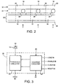
- Imaging devices comprising an array of image cells of various types are known.
- a semiconductor pixel detector which comprises a semiconductor substrate with electrodes which apply depletion voltage to each pixel position and define a charge collection volume.
- simple buffer circuits read out the electric signals when a photon is photo-absorbed or when ionising radiation crosses the depletion zone of the substrate. Accordingly pixel detectors of this type typically operate in a pulse mode, the numbers of hits being accumulated externally to the imaging device.
- the buffer circuits can either be on the same substrate (EP-A-0,287,197) as the charge collection volumes, or on a separate substrate (EP-A-0,571,135) that is mechanically bonded to a substrate having the charge collection volumes in accordance with, for example, the well known bump-bonding technique.
- an Active-pixel Semiconductor Imaging Device comprises an array of pixel cells including a semiconductor substrate having an array of pixel detectors and a further array of pixel circuits.
- the pixel detectors generate charge in response to instant radiation.
- Each pixel circuit is associated with a respective pixel detector and accumulates charge resulting from radiation incident on the pixel detector.
- the pixel circuits are individually addressable and comprise circuitry which enables charge to be accumulated from a plurality of successive radiation hits on the respective pixel detectors.
- the device operates by accumulating charge on the gate, for example, of a transistor. Accordingly, analogue storage of the charge value is obtained. At a determined time, the charge from the pixel circuits can be read out and used to generate an image based on the analogue charge values stored in each of the pixel circuits.
- CCD devices suffer from disadvantages of limited dynamic range, due to the limited capacity of the potential well inside the semiconductor substrate, and also to the inactive times during which an image is read out.
- Pulse counting semiconductive pixel devices also have the disadvantage of limited dynamic range. As these devices read the pixel contact when a hit is detected, they suffer from saturation problems at high counting rates.
- the semiconductor pixel device according to WO95/33332 provides significant advantages over the earlier prior art by providing a large dynamic range for the accumulation of images.
- the invention seeks to mitigate the problems of the prior art described above.
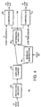
- the actual size of the pixel circuit and the pixel detector will depend on the application for which the imaging device is intended, and will also depend on the integrated circuit technology available for constructing the image circuit 20 to be described later. With current circuit technology, it is not possible to obtain the smallest possible image detectors which would be required in some applications. Typically, the minimum pixel size is of the order of 200 micrometres square using current technology. However, with advances expected in circuit manufacturing technology, it is expected that this minimum size can be significantly reduced using the teaching of the present application and improved circuit fabrication techniques. Accordingly, the present invention is not limited to any particular pixel image size.
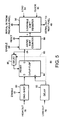
- FIG 4 is a schematic block diagram of the threshold circuitry 42 represented in Figure 3.
- protection circuitry 60 is connected to the input node 50 (ie the bump-bond connection 34 to the pixel detector 19).
- the protection circuitry is provided to prevent damage due to over- or under-voltage values and is typically provided by two diodes connected to the high and low supply line Vdd and Vss (not shown).
- the output of the protection circuitry 60 is connected to amplifier/shaper circuitry 62 which produces an analogue signal proportional to the charge injection of a delta peak.
- the amplifier shaper 62 is implemented by means of a charge sensitive amplifier followed by a shaper.
- the shaping time depends on the maximum signal rate on a pixel.
- Figure 4 illustrates optional baseline subtraction circuitry which is needed if the leakage current varies significantly within the selected shaping time.
- a differential amplifier 66 subtracts the baseline so that comparators 68 and 70 see the true peak signal height.
- First and second comparators 68 and 70 have respective high and low threshold values 72 and 74 input thereto.
- the high and low threshold values can represent higher and lower limits of accepted signal amplitudes. In this case any signal peaks below the low threshold and above the high threshold will be rejected by the counter circuitry 44. If the peak signal value exceeds the high threshold value 72, then the first comparator 68 outputs a logic 1, otherwise it outputs a logic 0.
- the second comparator 70 if the peak signal value exceeds the low threshold value 74, then the second comparator 70 outputs a logic 1, otherwise it outputs a logic 0. It will be appreciated that the comparison output values of the present embodiment form one example only and in other embodiments of the invention other values could be output as a result of the comparisons.
- the length of the single-triggered one-shot circuit 80 is adequate to coincide with the rising edge from the low output signal 78 from the second comparator 70 at all signal amplitudes.
- the high and low threshold values are supplied from the control logic 102 and are preferably adjustable.
- the high and low threshold values could be derived from the Vdd and Vss supply voltages in a fixed manner.
Landscapes
- Molecular Biology (AREA)
- Spectroscopy & Molecular Physics (AREA)
- High Energy & Nuclear Physics (AREA)
- Physics & Mathematics (AREA)
- Health & Medical Sciences (AREA)
- Life Sciences & Earth Sciences (AREA)
- General Physics & Mathematics (AREA)
- Multimedia (AREA)
- Engineering & Computer Science (AREA)
- Signal Processing (AREA)
- Transforming Light Signals Into Electric Signals (AREA)
- Measurement Of Radiation (AREA)
- Solid State Image Pick-Up Elements (AREA)
- Apparatus For Radiation Diagnosis (AREA)
- Light Receiving Elements (AREA)
- Facsimile Scanning Arrangements (AREA)
Applications Claiming Priority (3)
| Application Number | Priority Date | Filing Date | Title |
|---|---|---|---|
| GB9621470 | 1996-10-15 | ||
| GB9621470A GB2318411B (en) | 1996-10-15 | 1996-10-15 | Imaging device for imaging radiation |
| PCT/EP1997/005436 WO1998016853A1 (en) | 1996-10-15 | 1997-09-29 | Imaging device for imaging radiation |
Publications (2)
| Publication Number | Publication Date |
|---|---|
| EP0932842A1 EP0932842A1 (en) | 1999-08-04 |
| EP0932842B1 true EP0932842B1 (en) | 2002-04-10 |
Family
ID=10801442
Family Applications (1)
| Application Number | Title | Priority Date | Filing Date |
|---|---|---|---|
| EP97909356A Expired - Lifetime EP0932842B1 (en) | 1996-10-15 | 1997-09-29 | Imaging device for imaging radiation |
Country Status (12)
| Country | Link |
|---|---|
| US (3) | US6248990B1 (enExample) |
| EP (1) | EP0932842B1 (enExample) |
| JP (3) | JP2001502424A (enExample) |
| AT (1) | ATE216085T1 (enExample) |
| AU (1) | AU4707397A (enExample) |
| CA (1) | CA2268627A1 (enExample) |
| DE (1) | DE69711902T2 (enExample) |
| ES (1) | ES2175361T3 (enExample) |
| GB (1) | GB2318411B (enExample) |
| IL (1) | IL128703A (enExample) |
| NO (1) | NO991780L (enExample) |
| WO (1) | WO1998016853A1 (enExample) |
Cited By (1)
| Publication number | Priority date | Publication date | Assignee | Title |
|---|---|---|---|---|
| US7138635B2 (en) | 2003-11-07 | 2006-11-21 | Siemens Aktiengesellschaft | Detector module for CT and/or PET and/or SPECT tomography |
Families Citing this family (72)
| Publication number | Priority date | Publication date | Assignee | Title |
|---|---|---|---|---|
| GB2289983B (en) | 1994-06-01 | 1996-10-16 | Simage Oy | Imaging devices,systems and methods |
| GB2318411B (en) * | 1996-10-15 | 1999-03-10 | Simage Oy | Imaging device for imaging radiation |
| CA2347526A1 (en) * | 1998-10-19 | 2000-04-27 | Ben-Gurion University Of The Negev | Optical imager using a method for adaptive real-time expanding of the dynamic range |
| US9029793B2 (en) | 1998-11-05 | 2015-05-12 | Siemens Aktiengesellschaft | Imaging device |
| GB2343577B (en) * | 1998-11-05 | 2001-01-24 | Simage Oy | Imaging device |
| FR2791469B1 (fr) * | 1999-03-23 | 2001-04-13 | Commissariat Energie Atomique | Dispositif d'imagerie de rayonnement x et procede de realisation d'un tel dispositif |
| GB2357414A (en) * | 1999-12-16 | 2001-06-20 | Secr Defence | Fast detection of X-rays using detector arrays and energy discrimination |
| FI111759B (fi) * | 2000-03-14 | 2003-09-15 | Planmed Oy | Anturijärjestelmä ja menetelmä digitaalisessa röntgenkuvantamisessa |
| US6307915B1 (en) * | 2000-06-26 | 2001-10-23 | Afp Imaging Corporation | Triggering of solid state X-ray imagers with non-destructive readout capability |
| DE10033179B4 (de) * | 2000-06-29 | 2016-06-02 | Carl Zeiss Microscopy Gmbh | Verfahren zur optischen Detektion einer beleuchteten Probe in mehreren Detektionskanälen |
| US6747737B2 (en) * | 2000-06-29 | 2004-06-08 | Carl Zeiss Jena Gmbh | Method for optical detection of an illuminated specimen in a plurality of detection channels |
| US6795118B1 (en) * | 2000-10-18 | 2004-09-21 | Micron Technology, Inc. | Testing of solid-state image sensors |
| WO2002057807A1 (en) * | 2000-10-24 | 2002-07-25 | Ii-Vi Incorporated | High-speed pulse discriminating gamma ray camera |
| US6642495B2 (en) * | 2001-02-12 | 2003-11-04 | Princeton Scientific Instruments | Optical pulse counting imager and system |
| US20040212017A1 (en) * | 2001-08-07 | 2004-10-28 | Hirotaka Mizuno | Semiconductor device and ic card |
| US6677569B2 (en) * | 2001-10-12 | 2004-01-13 | Massachusetts Institute Of Technology | Methods and apparatus for performing signal processing functions in an electronic imager |
| FI119173B (fi) * | 2001-11-23 | 2008-08-29 | Planmed Oy | Anturijärjestely ja menetelmä digitaalisessa pyyhkäisykuvantamisessa |
| US7412022B2 (en) * | 2002-02-28 | 2008-08-12 | Jupiter Clyde P | Non-invasive stationary system for three-dimensional imaging of density fields using periodic flux modulation of compton-scattered gammas |
| US7361881B2 (en) * | 2002-03-13 | 2008-04-22 | Oy Ajat Ltd | Ganged detector pixel, photon/pulse counting radiation imaging device |
| DE10212638A1 (de) * | 2002-03-21 | 2003-10-16 | Siemens Ag | Computertomograph und Verfahren zum Nachweis von Röntgenstrahlung mit einer aus einer Vielzahl von Detektoren bestehenden Detektoreinheit |
| FI20021255A7 (fi) * | 2002-06-27 | 2003-12-28 | Metorex Int Oy | Suoraan konversioon perustuva kuvaava röntgendetektori ja sellaista käyttävä kuvausjärjestely |
| GB0224689D0 (en) | 2002-10-23 | 2002-12-04 | Simage Oy | Formation of contacts on semiconductor substrates |
| WO2004038810A2 (en) | 2002-10-25 | 2004-05-06 | Goldpower Limited | Circuit substrate and method |
| US7223981B1 (en) * | 2002-12-04 | 2007-05-29 | Aguila Technologies Inc. | Gamma ray detector modules |
| ES2327835T3 (es) | 2003-01-10 | 2009-11-04 | Paul Scherrer Institut | Dispositivo de imagenes de recuento de fotones. |
| WO2004095060A2 (en) * | 2003-04-23 | 2004-11-04 | L-3 Communications Security and Detection Systems Corporation | X-ray imaging technique |
| US7130379B2 (en) * | 2003-05-28 | 2006-10-31 | International Business Machines Corporation | Device and method for generating an x-ray point source by geometric confinement |
| US7332724B2 (en) * | 2005-07-26 | 2008-02-19 | General Electric Company | Method and apparatus for acquiring radiation data |
| US7202463B1 (en) * | 2005-09-16 | 2007-04-10 | Adobe Systems Incorporated | Higher dynamic range image sensor with signal integration |
| US7605375B2 (en) * | 2007-04-26 | 2009-10-20 | Oy Ajat Ltd. | Multi-functional radiation/photon identifying and processing application specific integrated circuit and device |
| FR2916117B1 (fr) * | 2007-05-10 | 2011-03-18 | Centre Nat Rech Scient | Dispositif d'imagerie par rayons x a source poly-chromatique |
| EP2028509A1 (en) * | 2007-08-09 | 2009-02-25 | European Organisation for Nuclear Research CERN | Radiation monitoring device |
| JP2008175829A (ja) * | 2008-02-25 | 2008-07-31 | Toshiba Corp | 粒子線測定方法および粒子線測定用モニタ装置 |
| JP5124332B2 (ja) * | 2008-03-31 | 2013-01-23 | 株式会社日立製作所 | 放射線検査装置及び校正方法 |
| JP2010078338A (ja) * | 2008-09-24 | 2010-04-08 | Toshiba Corp | X線検出器 |
| US8422629B2 (en) * | 2009-03-27 | 2013-04-16 | Weyerhaeuser Nr Company | Seedling counter |
| EP2427112A4 (en) * | 2009-05-08 | 2016-07-13 | L 3 Comm Security & Detection | BIENERGY IMAGING SYSTEM |
| FI122647B (fi) | 2009-06-09 | 2012-05-15 | Planmeca Oy | Digitaaliröntgenanturijärjestely ja digitaalinen röntgenkuvantamismenetelmä |
| US8384038B2 (en) * | 2009-06-24 | 2013-02-26 | General Electric Company | Readout electronics for photon counting and energy discriminating detectors |
| EP2348704A1 (en) * | 2010-01-26 | 2011-07-27 | Paul Scherrer Institut | A single photon counting readout chip with neglibible dead time |
| US8716643B2 (en) * | 2010-09-06 | 2014-05-06 | King Abdulaziz City Science And Technology | Single photon counting image sensor and method |
| EP2651119B1 (en) | 2010-12-09 | 2017-02-22 | Rigaku Corporation | Radiation detector |
| DE102011003454A1 (de) * | 2011-02-01 | 2012-08-02 | Siemens Aktiengesellschaft | Strahlungsdirektkonverter, Strahlungsdetektor, medizintechnisches Gerät und Verfahren zum Erzeugen eines Strahlungsdirektkonverters |
| EP2490441A1 (en) * | 2011-02-16 | 2012-08-22 | Paul Scherrer Institut | Single photon counting detector system having improved counter architecture |
| US9052497B2 (en) | 2011-03-10 | 2015-06-09 | King Abdulaziz City For Science And Technology | Computing imaging data using intensity correlation interferometry |
| US9099214B2 (en) | 2011-04-19 | 2015-08-04 | King Abdulaziz City For Science And Technology | Controlling microparticles through a light field having controllable intensity and periodicity of maxima thereof |
| US9310495B2 (en) | 2011-05-04 | 2016-04-12 | Oy Ajat Ltd. | Photon/energy identifying X-ray and gamma ray imaging device (“PID”) with a two dimensional array of pixels and system therefrom |
| US8488854B2 (en) * | 2011-12-07 | 2013-07-16 | Ge Medical Systems Israel, Ltd. | System and apparatus for classifying x-ray energy into discrete levels |
| US9069092B2 (en) | 2012-02-22 | 2015-06-30 | L-3 Communication Security and Detection Systems Corp. | X-ray imager with sparse detector array |
| DE102012212124B4 (de) | 2012-07-11 | 2018-06-14 | Siemens Healthcare Gmbh | Zählender digitaler Röntgendetektor und Verfahren zur Aufnahme einer Serie von Röntgenbildern |
| US9036065B1 (en) * | 2012-08-16 | 2015-05-19 | Rambus Inc. | Shared-counter image sensor |
| EP2871496B1 (en) | 2013-11-12 | 2020-01-01 | Samsung Electronics Co., Ltd | Radiation detector and computed tomography apparatus using the same |
| CN106291653B (zh) * | 2015-06-29 | 2019-04-23 | 中国辐射防护研究院 | 流体总α、总β放射性连续在线监测方法及装置 |
| CN107300712B (zh) * | 2016-04-14 | 2021-08-17 | 中国辐射防护研究院 | 一种可同时测量β、γ能谱的层叠型闪烁体探测器的测量方法 |
| SE542767C2 (en) * | 2018-05-15 | 2020-07-07 | Xcounter Ab | Sensor unit and radiation detector |
| JP7232001B2 (ja) * | 2018-08-27 | 2023-03-02 | キヤノン株式会社 | 撮像素子及びその制御方法、プログラム、記憶媒体 |
| US11985440B2 (en) | 2018-11-12 | 2024-05-14 | Magic Leap, Inc. | Depth based dynamic vision sensor |
| WO2020101895A1 (en) | 2018-11-12 | 2020-05-22 | Magic Leap, Inc. | Event-based camera with high-resolution frame output |
| US11902677B2 (en) | 2018-11-12 | 2024-02-13 | Magic Leap, Inc. | Patch tracking image sensor |
| WO2020102110A1 (en) * | 2018-11-13 | 2020-05-22 | Magic Leap, Inc. | Event-based ir camera |
| US11889209B2 (en) | 2019-02-07 | 2024-01-30 | Magic Leap, Inc. | Lightweight cross reality device with passive depth extraction |
| CN113678435B (zh) | 2019-02-07 | 2025-05-06 | 奇跃公司 | 具有高时间分辨率的轻型低功耗交叉现实设备 |
| DE102019111567A1 (de) * | 2019-05-03 | 2020-11-05 | Wipotec Gmbh | Verfahren und Vorrichtung zur Röntgeninspektion von Produkten, insbesondere von Lebensmitteln |
| EP3756033B1 (en) | 2019-05-13 | 2023-11-15 | Varex Imaging Sweden AB | Method of reading out data in a radiation detector, radiation detector and imaging apparatus |
| TW202141064A (zh) * | 2020-03-24 | 2021-11-01 | 日商索尼半導體解決方案公司 | 受光裝置及測距裝置 |
| WO2022074732A1 (ja) * | 2020-10-06 | 2022-04-14 | 国立大学法人静岡大学 | 放射線撮像装置 |
| WO2022109868A1 (en) * | 2020-11-25 | 2022-06-02 | Shenzhen Xpectvision Technology Co., Ltd. | Imaging apparatus |
| DE112021005839T5 (de) * | 2020-12-09 | 2023-08-17 | Ams International Ag | Elektrische schaltung zur extraktion der baseline in einem photonenzählsystem |
| CN112711060B (zh) * | 2020-12-18 | 2022-10-04 | 兰州大学 | 一种多层闪烁体β-γ混合场探测器探头 |
| KR102368868B1 (ko) * | 2021-07-26 | 2022-03-04 | 한전케이피에스 주식회사 | 컴프턴 산란을 이용하는 파이프용 검사 장치 |
| JP7743465B2 (ja) * | 2023-05-30 | 2025-09-24 | キヤノン株式会社 | 光電変換装置、移動体、光電変換方法、及びコンピュータプログラム |
| EP4617732A1 (de) * | 2024-03-14 | 2025-09-17 | Siemens Healthineers AG | Photonenzählender röntgendetektor, verfahren zum betreiben eines photonenzählenden röntgendetektors und röntgengerät |
Family Cites Families (33)
| Publication number | Priority date | Publication date | Assignee | Title |
|---|---|---|---|---|
| US4131798A (en) * | 1977-04-05 | 1978-12-26 | Abbott Laboratories | Array gamma counter |
| JPS57149979A (en) * | 1981-03-11 | 1982-09-16 | Mitsubishi Electric Corp | Single channel frequency meter |
| JPH0640077B2 (ja) * | 1983-10-12 | 1994-05-25 | 松下電器産業株式会社 | 放射線受像方法 |
| JPS60164287A (ja) * | 1984-02-07 | 1985-08-27 | Rigaku Denki Kogyo Kk | パルス波高値分析装置 |
| JPS614989A (ja) * | 1984-06-19 | 1986-01-10 | Matsushita Electric Ind Co Ltd | 放射線線量率計 |
| JPH0799868B2 (ja) * | 1984-12-26 | 1995-10-25 | 日本放送協会 | 固体撮像装置 |
| JPS6295484A (ja) * | 1985-10-22 | 1987-05-01 | Denki Kagaku Keiki Co Ltd | 基線安定化回路 |
| JPH0612560Y2 (ja) * | 1985-12-31 | 1994-03-30 | 株式会社島津製作所 | 放射線パイルアツプ検出回路 |
| JPS62191787A (ja) * | 1986-02-18 | 1987-08-22 | Matsushita Electric Ind Co Ltd | 放射線受像装置 |
| US4804854A (en) * | 1987-02-16 | 1989-02-14 | Shimadzu Corporation | Low-noise arrayed sensor radiation image detecting system wherein each sensor connects to a buffer circuit |
| JPH01138485A (ja) * | 1987-11-25 | 1989-05-31 | Matsushita Electric Ind Co Ltd | 放射線画像装置 |
| JPH01216290A (ja) * | 1988-02-24 | 1989-08-30 | Shimadzu Corp | 半導体放射線位置検出器とその製造方法 |
| JPH01264154A (ja) * | 1988-04-14 | 1989-10-20 | Matsushita Electric Ind Co Ltd | 放射線受像装置 |
| JPH036966A (ja) * | 1989-06-02 | 1991-01-14 | Fuji Electric Co Ltd | Ccdイメージセンサ |
| JPH0317587A (ja) * | 1989-06-14 | 1991-01-25 | Fuji Electric Co Ltd | 半導体放射線測定装置 |
| JPH0715499B2 (ja) * | 1989-06-23 | 1995-02-22 | 松下電器産業株式会社 | 放射線受像装置 |
| JP2890553B2 (ja) * | 1989-11-24 | 1999-05-17 | 株式会社島津製作所 | X線像撮像装置 |
| JPH03233384A (ja) * | 1990-02-09 | 1991-10-17 | Hitachi Medical Corp | ポジトロンct用偶発同時計数回路 |
| US5107122A (en) * | 1990-10-12 | 1992-04-21 | Hughes Aircraft Company | Sparse readout method and apparatus for a pixel array |
| GB2262383B (en) * | 1991-12-09 | 1995-06-14 | Sony Broadcast & Communication | Charge-coupled image sensor |
| CA2095366C (en) * | 1992-05-21 | 1999-09-14 | Timothy C. Collins | Hybridized semiconductor pixel detector arrays for use in digital radiography |
| US5235176A (en) * | 1992-07-30 | 1993-08-10 | General Electric Company | Optical radiation sensing assembly with increased resolution |
| JPH06148332A (ja) * | 1992-11-02 | 1994-05-27 | Toshiba Corp | 宇宙線データ収集装置 |
| JP2604114Y2 (ja) * | 1993-11-30 | 2000-04-17 | 株式会社島津製作所 | 放射線検出器 |
| US5493122A (en) * | 1994-02-04 | 1996-02-20 | Nucleonics Development Company | Energy resolving x-ray detector |
| GB2289979A (en) * | 1994-06-01 | 1995-12-06 | Simage Oy | Imaging devices systems and methods |
| GB2289983B (en) * | 1994-06-01 | 1996-10-16 | Simage Oy | Imaging devices,systems and methods |
| KR987001092A (ko) * | 1994-12-23 | 1998-04-30 | 엘. 린그렌 클린턴 | 반도체 감마 선 카메라 및 의학 화상 시스템(Semiconductor Gamma-Ray Camera and Medical Imaging System) |
| WO1996041213A1 (en) * | 1995-06-07 | 1996-12-19 | Massachusetts Institute Of Technology | X-ray detector and method for measuring energy of individual x-ray photons for improved imaging of subjects using reduced dose |
| JP3643432B2 (ja) * | 1996-04-10 | 2005-04-27 | 株式会社東芝 | 核医学診断装置 |
| JPH1033518A (ja) * | 1996-07-26 | 1998-02-10 | Toshiba Corp | X線診断装置 |
| US5742659A (en) * | 1996-08-26 | 1998-04-21 | Universities Research Assoc., Inc. | High resolution biomedical imaging system with direct detection of x-rays via a charge coupled device |
| GB2318411B (en) * | 1996-10-15 | 1999-03-10 | Simage Oy | Imaging device for imaging radiation |
-
1996
- 1996-10-15 GB GB9621470A patent/GB2318411B/en not_active Expired - Fee Related
-
1997
- 1997-09-29 AU AU47073/97A patent/AU4707397A/en not_active Abandoned
- 1997-09-29 JP JP10517972A patent/JP2001502424A/ja active Pending
- 1997-09-29 CA CA002268627A patent/CA2268627A1/en not_active Abandoned
- 1997-09-29 EP EP97909356A patent/EP0932842B1/en not_active Expired - Lifetime
- 1997-09-29 IL IL12870397A patent/IL128703A/en not_active IP Right Cessation
- 1997-09-29 ES ES97909356T patent/ES2175361T3/es not_active Expired - Lifetime
- 1997-09-29 DE DE69711902T patent/DE69711902T2/de not_active Expired - Lifetime
- 1997-09-29 WO PCT/EP1997/005436 patent/WO1998016853A1/en not_active Ceased
- 1997-09-29 AT AT97909356T patent/ATE216085T1/de active
- 1997-10-10 US US08/948,778 patent/US6248990B1/en not_active Expired - Lifetime
-
1999
- 1999-04-14 NO NO991780A patent/NO991780L/no unknown
-
2001
- 2001-04-25 US US09/840,870 patent/US6355923B2/en not_active Expired - Lifetime
-
2002
- 2002-03-11 US US10/096,136 patent/US20020092970A1/en not_active Abandoned
-
2011
- 2011-03-28 JP JP2011070578A patent/JP5623954B2/ja not_active Expired - Lifetime
-
2014
- 2014-07-31 JP JP2014156912A patent/JP5800966B2/ja not_active Expired - Lifetime
Cited By (1)
| Publication number | Priority date | Publication date | Assignee | Title |
|---|---|---|---|---|
| US7138635B2 (en) | 2003-11-07 | 2006-11-21 | Siemens Aktiengesellschaft | Detector module for CT and/or PET and/or SPECT tomography |
Also Published As
| Publication number | Publication date |
|---|---|
| DE69711902T2 (de) | 2002-11-14 |
| AU4707397A (en) | 1998-05-11 |
| JP2011174936A (ja) | 2011-09-08 |
| DE69711902D1 (de) | 2002-05-16 |
| NO991780L (no) | 1999-06-15 |
| US6248990B1 (en) | 2001-06-19 |
| CA2268627A1 (en) | 1998-04-23 |
| GB9621470D0 (en) | 1996-12-04 |
| US6355923B2 (en) | 2002-03-12 |
| NO991780D0 (no) | 1999-04-14 |
| IL128703A (en) | 2004-06-20 |
| US20020092970A1 (en) | 2002-07-18 |
| JP2001502424A (ja) | 2001-02-20 |
| EP0932842A1 (en) | 1999-08-04 |
| ES2175361T3 (es) | 2002-11-16 |
| US20010025914A1 (en) | 2001-10-04 |
| JP5623954B2 (ja) | 2014-11-12 |
| JP5800966B2 (ja) | 2015-10-28 |
| JP2015004681A (ja) | 2015-01-08 |
| GB2318411B (en) | 1999-03-10 |
| ATE216085T1 (de) | 2002-04-15 |
| HK1010577A1 (en) | 1999-06-25 |
| IL128703A0 (en) | 2000-01-31 |
| WO1998016853A1 (en) | 1998-04-23 |
| GB2318411A (en) | 1998-04-22 |
Similar Documents
| Publication | Publication Date | Title |
|---|---|---|
| EP0932842B1 (en) | Imaging device for imaging radiation | |
| US6657200B2 (en) | Readout system for solid-state detector arrays | |
| US6690019B2 (en) | High data rate smart sensor | |
| JP5701743B2 (ja) | 放射線検出器、画像システム、光子を検出するための方法及びその方法を実行するコンピュータプログラム | |
| US9310495B2 (en) | Photon/energy identifying X-ray and gamma ray imaging device (“PID”) with a two dimensional array of pixels and system therefrom | |
| US6856350B2 (en) | Semiconductor radiation imaging device including threshold circuitry | |
| EP1127454B1 (en) | Imaging device using Time Delay Integration and radiation hit counts | |
| US9029793B2 (en) | Imaging device | |
| EP1064780B1 (en) | Imaging device for imaging radiation | |
| US9201150B2 (en) | Suppression of direct detection events in X-ray detectors | |
| US6586743B1 (en) | X-ray detector having sensors and evaluation units | |
| US5619040A (en) | Data acquisition system | |
| JPH095445A (ja) | 放射線像撮像装置 | |
| Allison | Cadmium telluride matrix gamma camera |
Legal Events
| Date | Code | Title | Description |
|---|---|---|---|
| PUAI | Public reference made under article 153(3) epc to a published international application that has entered the european phase |
Free format text: ORIGINAL CODE: 0009012 |
|
| 17P | Request for examination filed |
Effective date: 19990219 |
|
| AK | Designated contracting states |
Kind code of ref document: A1 Designated state(s): AT BE CH DE DK ES FI FR GB GR IE IT LI LU MC NL PT SE |
|
| 17Q | First examination report despatched |
Effective date: 20000710 |
|
| RAP1 | Party data changed (applicant data changed or rights of an application transferred) |
Owner name: SIMAGE OY |
|
| GRAG | Despatch of communication of intention to grant |
Free format text: ORIGINAL CODE: EPIDOS AGRA |
|
| GRAG | Despatch of communication of intention to grant |
Free format text: ORIGINAL CODE: EPIDOS AGRA |
|
| GRAH | Despatch of communication of intention to grant a patent |
Free format text: ORIGINAL CODE: EPIDOS IGRA |
|
| REG | Reference to a national code |
Ref country code: GB Ref legal event code: IF02 |
|
| GRAH | Despatch of communication of intention to grant a patent |
Free format text: ORIGINAL CODE: EPIDOS IGRA |
|
| GRAA | (expected) grant |
Free format text: ORIGINAL CODE: 0009210 |
|
| AK | Designated contracting states |
Kind code of ref document: B1 Designated state(s): AT BE CH DE DK ES FI FR GB GR IE IT LI LU MC NL PT SE |
|
| PG25 | Lapsed in a contracting state [announced via postgrant information from national office to epo] |
Ref country code: LI Free format text: LAPSE BECAUSE OF FAILURE TO SUBMIT A TRANSLATION OF THE DESCRIPTION OR TO PAY THE FEE WITHIN THE PRESCRIBED TIME-LIMIT Effective date: 20020410 Ref country code: GR Free format text: LAPSE BECAUSE OF FAILURE TO SUBMIT A TRANSLATION OF THE DESCRIPTION OR TO PAY THE FEE WITHIN THE PRESCRIBED TIME-LIMIT Effective date: 20020410 Ref country code: CH Free format text: LAPSE BECAUSE OF FAILURE TO SUBMIT A TRANSLATION OF THE DESCRIPTION OR TO PAY THE FEE WITHIN THE PRESCRIBED TIME-LIMIT Effective date: 20020410 Ref country code: BE Free format text: LAPSE BECAUSE OF FAILURE TO SUBMIT A TRANSLATION OF THE DESCRIPTION OR TO PAY THE FEE WITHIN THE PRESCRIBED TIME-LIMIT Effective date: 20020410 Ref country code: AT Free format text: LAPSE BECAUSE OF FAILURE TO SUBMIT A TRANSLATION OF THE DESCRIPTION OR TO PAY THE FEE WITHIN THE PRESCRIBED TIME-LIMIT Effective date: 20020410 |
|
| REF | Corresponds to: |
Ref document number: 216085 Country of ref document: AT Date of ref document: 20020415 Kind code of ref document: T |
|
| REG | Reference to a national code |
Ref country code: CH Ref legal event code: EP |
|
| REG | Reference to a national code |
Ref country code: IE Ref legal event code: FG4D |
|
| REF | Corresponds to: |
Ref document number: 69711902 Country of ref document: DE Date of ref document: 20020516 |
|
| PG25 | Lapsed in a contracting state [announced via postgrant information from national office to epo] |
Ref country code: SE Free format text: LAPSE BECAUSE OF FAILURE TO SUBMIT A TRANSLATION OF THE DESCRIPTION OR TO PAY THE FEE WITHIN THE PRESCRIBED TIME-LIMIT Effective date: 20020710 Ref country code: PT Free format text: LAPSE BECAUSE OF FAILURE TO SUBMIT A TRANSLATION OF THE DESCRIPTION OR TO PAY THE FEE WITHIN THE PRESCRIBED TIME-LIMIT Effective date: 20020710 Ref country code: DK Free format text: LAPSE BECAUSE OF FAILURE TO SUBMIT A TRANSLATION OF THE DESCRIPTION OR TO PAY THE FEE WITHIN THE PRESCRIBED TIME-LIMIT Effective date: 20020710 |
|
| PGFP | Annual fee paid to national office [announced via postgrant information from national office to epo] |
Ref country code: ES Payment date: 20020909 Year of fee payment: 6 |
|
| PG25 | Lapsed in a contracting state [announced via postgrant information from national office to epo] |
Ref country code: LU Free format text: LAPSE BECAUSE OF NON-PAYMENT OF DUE FEES Effective date: 20020929 |
|
| PG25 | Lapsed in a contracting state [announced via postgrant information from national office to epo] |
Ref country code: IE Free format text: LAPSE BECAUSE OF NON-PAYMENT OF DUE FEES Effective date: 20020930 |
|
| ET | Fr: translation filed | ||
| REG | Reference to a national code |
Ref country code: CH Ref legal event code: PL |
|
| REG | Reference to a national code |
Ref country code: ES Ref legal event code: FG2A Ref document number: 2175361 Country of ref document: ES Kind code of ref document: T3 |
|
| PLBE | No opposition filed within time limit |
Free format text: ORIGINAL CODE: 0009261 |
|
| STAA | Information on the status of an ep patent application or granted ep patent |
Free format text: STATUS: NO OPPOSITION FILED WITHIN TIME LIMIT |
|
| PG25 | Lapsed in a contracting state [announced via postgrant information from national office to epo] |
Ref country code: MC Free format text: LAPSE BECAUSE OF NON-PAYMENT OF DUE FEES Effective date: 20030401 |
|
| 26N | No opposition filed |
Effective date: 20030113 |
|
| REG | Reference to a national code |
Ref country code: IE Ref legal event code: MM4A |
|
| PG25 | Lapsed in a contracting state [announced via postgrant information from national office to epo] |
Ref country code: ES Free format text: LAPSE BECAUSE OF NON-PAYMENT OF DUE FEES Effective date: 20030930 |
|
| REG | Reference to a national code |
Ref country code: ES Ref legal event code: FD2A Effective date: 20030930 |
|
| REG | Reference to a national code |
Ref country code: GB Ref legal event code: 732E |
|
| NLS | Nl: assignments of ep-patents |
Owner name: GOLDPOWER LIMITED |
|
| PG25 | Lapsed in a contracting state [announced via postgrant information from national office to epo] |
Ref country code: IT Free format text: LAPSE BECAUSE OF NON-PAYMENT OF DUE FEES Effective date: 20050929 |
|
| REG | Reference to a national code |
Ref country code: FR Ref legal event code: TP |
|
| REG | Reference to a national code |
Ref country code: GB Ref legal event code: 732E |
|
| REG | Reference to a national code |
Ref country code: GB Ref legal event code: 732E |
|
| NLS | Nl: assignments of ep-patents |
Owner name: IPL INTELLECTUAL PROPERTY LICENSING LIMITED Effective date: 20070626 |
|
| NLUE | Nl: licence registered with regard to european patents |
Effective date: 20070626 |
|
| REG | Reference to a national code |
Ref country code: FR Ref legal event code: TP Ref country code: FR Ref legal event code: CL |
|
| REG | Reference to a national code |
Ref country code: NL Ref legal event code: UDE Effective date: 20110301 |
|
| REG | Reference to a national code |
Ref country code: FR Ref legal event code: RL |
|
| REG | Reference to a national code |
Ref country code: DE Ref legal event code: R089 Ref document number: 69711902 Country of ref document: DE |
|
| REG | Reference to a national code |
Ref country code: GB Ref legal event code: 732E Free format text: REGISTERED BETWEEN 20110414 AND 20110420 |
|
| REG | Reference to a national code |
Ref country code: FR Ref legal event code: TP |
|
| REG | Reference to a national code |
Ref country code: NL Ref legal event code: SD Effective date: 20110504 |
|
| REG | Reference to a national code |
Ref country code: DE Ref legal event code: R082 Ref document number: 69711902 Country of ref document: DE Ref country code: DE Ref legal event code: R081 Ref document number: 69711902 Country of ref document: DE Owner name: SIEMENS HEALTHCARE GMBH, DE Free format text: FORMER OWNER: IPL INTELLECTUAL PROPERTY LICENSING LTD., LIMASSOL, CY Ref country code: DE Ref legal event code: R081 Ref document number: 69711902 Country of ref document: DE Owner name: SIEMENS AKTIENGESELLSCHAFT, DE Free format text: FORMER OWNER: IPL INTELLECTUAL PROPERTY LICENSING LTD., LIMASSOL, CY |
|
| REG | Reference to a national code |
Ref country code: DE Ref legal event code: R082 Ref document number: 69711902 Country of ref document: DE Ref country code: DE Ref legal event code: R081 Ref document number: 69711902 Country of ref document: DE Owner name: SIEMENS HEALTHCARE GMBH, DE Free format text: FORMER OWNER: SIEMENS AKTIENGESELLSCHAFT, 80333 MUENCHEN, DE Ref country code: DE Ref legal event code: R081 Ref document number: 69711902 Country of ref document: DE Owner name: SIEMENS AKTIENGESELLSCHAFT, DE Free format text: FORMER OWNER: SIEMENS AKTIENGESELLSCHAFT, 80333 MUENCHEN, DE |
|
| REG | Reference to a national code |
Ref country code: DE Ref legal event code: R081 Ref document number: 69711902 Country of ref document: DE Owner name: SIEMENS HEALTHCARE GMBH, DE Free format text: FORMER OWNER: SIEMENS AKTIENGESELLSCHAFT, 80333 MUENCHEN, DE |
|
| REG | Reference to a national code |
Ref country code: FR Ref legal event code: PLFP Year of fee payment: 20 |
|
| PGFP | Annual fee paid to national office [announced via postgrant information from national office to epo] |
Ref country code: GB Payment date: 20160914 Year of fee payment: 20 Ref country code: FI Payment date: 20160913 Year of fee payment: 20 Ref country code: NL Payment date: 20160905 Year of fee payment: 20 |
|
| PGFP | Annual fee paid to national office [announced via postgrant information from national office to epo] |
Ref country code: FR Payment date: 20160914 Year of fee payment: 20 |
|
| PGFP | Annual fee paid to national office [announced via postgrant information from national office to epo] |
Ref country code: DE Payment date: 20161121 Year of fee payment: 20 |
|
| REG | Reference to a national code |
Ref country code: DE Ref legal event code: R071 Ref document number: 69711902 Country of ref document: DE |
|
| REG | Reference to a national code |
Ref country code: NL Ref legal event code: MK Effective date: 20170928 |
|
| REG | Reference to a national code |
Ref country code: GB Ref legal event code: PE20 Expiry date: 20170928 |
|
| PG25 | Lapsed in a contracting state [announced via postgrant information from national office to epo] |
Ref country code: GB Free format text: LAPSE BECAUSE OF EXPIRATION OF PROTECTION Effective date: 20170928 |