EP0907928B1 - Systemträger für die montage einer integrierten schaltung in einem spritzgussgehäuse - Google Patents
Systemträger für die montage einer integrierten schaltung in einem spritzgussgehäuse Download PDFInfo
- Publication number
- EP0907928B1 EP0907928B1 EP97931650A EP97931650A EP0907928B1 EP 0907928 B1 EP0907928 B1 EP 0907928B1 EP 97931650 A EP97931650 A EP 97931650A EP 97931650 A EP97931650 A EP 97931650A EP 0907928 B1 EP0907928 B1 EP 0907928B1
- Authority
- EP
- European Patent Office
- Prior art keywords
- spring element
- lead
- injection
- housing
- integrated circuit
- Prior art date
- Legal status (The legal status is an assumption and is not a legal conclusion. Google has not performed a legal analysis and makes no representation as to the accuracy of the status listed.)
- Expired - Lifetime
Links
Images
Classifications
-
- G—PHYSICS
- G06—COMPUTING OR CALCULATING; COUNTING
- G06K—GRAPHICAL DATA READING; PRESENTATION OF DATA; RECORD CARRIERS; HANDLING RECORD CARRIERS
- G06K19/00—Record carriers for use with machines and with at least a part designed to carry digital markings
- G06K19/06—Record carriers for use with machines and with at least a part designed to carry digital markings characterised by the kind of the digital marking, e.g. shape, nature, code
- G06K19/067—Record carriers with conductive marks, printed circuits or semiconductor circuit elements, e.g. credit or identity cards also with resonating or responding marks without active components
- G06K19/07—Record carriers with conductive marks, printed circuits or semiconductor circuit elements, e.g. credit or identity cards also with resonating or responding marks without active components with integrated circuit chips
- G06K19/077—Constructional details, e.g. mounting of circuits in the carrier
- G06K19/0772—Physical layout of the record carrier
- G06K19/07724—Physical layout of the record carrier the record carrier being at least partially made by a molding process
-
- H—ELECTRICITY
- H01—ELECTRIC ELEMENTS
- H01L—SEMICONDUCTOR DEVICES NOT COVERED BY CLASS H10
- H01L23/00—Details of semiconductor or other solid state devices
-
- G—PHYSICS
- G06—COMPUTING OR CALCULATING; COUNTING
- G06K—GRAPHICAL DATA READING; PRESENTATION OF DATA; RECORD CARRIERS; HANDLING RECORD CARRIERS
- G06K19/00—Record carriers for use with machines and with at least a part designed to carry digital markings
- G06K19/06—Record carriers for use with machines and with at least a part designed to carry digital markings characterised by the kind of the digital marking, e.g. shape, nature, code
- G06K19/067—Record carriers with conductive marks, printed circuits or semiconductor circuit elements, e.g. credit or identity cards also with resonating or responding marks without active components
- G06K19/07—Record carriers with conductive marks, printed circuits or semiconductor circuit elements, e.g. credit or identity cards also with resonating or responding marks without active components with integrated circuit chips
- G06K19/077—Constructional details, e.g. mounting of circuits in the carrier
- G06K19/07743—External electrical contacts
-
- G—PHYSICS
- G06—COMPUTING OR CALCULATING; COUNTING
- G06K—GRAPHICAL DATA READING; PRESENTATION OF DATA; RECORD CARRIERS; HANDLING RECORD CARRIERS
- G06K19/00—Record carriers for use with machines and with at least a part designed to carry digital markings
- G06K19/06—Record carriers for use with machines and with at least a part designed to carry digital markings characterised by the kind of the digital marking, e.g. shape, nature, code
- G06K19/067—Record carriers with conductive marks, printed circuits or semiconductor circuit elements, e.g. credit or identity cards also with resonating or responding marks without active components
- G06K19/07—Record carriers with conductive marks, printed circuits or semiconductor circuit elements, e.g. credit or identity cards also with resonating or responding marks without active components with integrated circuit chips
- G06K19/077—Constructional details, e.g. mounting of circuits in the carrier
- G06K19/07745—Mounting details of integrated circuit chips
-
- H—ELECTRICITY
- H01—ELECTRIC ELEMENTS
- H01L—SEMICONDUCTOR DEVICES NOT COVERED BY CLASS H10
- H01L2224/00—Indexing scheme for arrangements for connecting or disconnecting semiconductor or solid-state bodies and methods related thereto as covered by H01L24/00
- H01L2224/01—Means for bonding being attached to, or being formed on, the surface to be connected, e.g. chip-to-package, die-attach, "first-level" interconnects; Manufacturing methods related thereto
- H01L2224/26—Layer connectors, e.g. plate connectors, solder or adhesive layers; Manufacturing methods related thereto
- H01L2224/31—Structure, shape, material or disposition of the layer connectors after the connecting process
- H01L2224/32—Structure, shape, material or disposition of the layer connectors after the connecting process of an individual layer connector
- H01L2224/321—Disposition
- H01L2224/32151—Disposition the layer connector connecting between a semiconductor or solid-state body and an item not being a semiconductor or solid-state body, e.g. chip-to-substrate, chip-to-passive
- H01L2224/32221—Disposition the layer connector connecting between a semiconductor or solid-state body and an item not being a semiconductor or solid-state body, e.g. chip-to-substrate, chip-to-passive the body and the item being stacked
- H01L2224/32245—Disposition the layer connector connecting between a semiconductor or solid-state body and an item not being a semiconductor or solid-state body, e.g. chip-to-substrate, chip-to-passive the body and the item being stacked the item being metallic
-
- H—ELECTRICITY
- H01—ELECTRIC ELEMENTS
- H01L—SEMICONDUCTOR DEVICES NOT COVERED BY CLASS H10
- H01L2224/00—Indexing scheme for arrangements for connecting or disconnecting semiconductor or solid-state bodies and methods related thereto as covered by H01L24/00
- H01L2224/01—Means for bonding being attached to, or being formed on, the surface to be connected, e.g. chip-to-package, die-attach, "first-level" interconnects; Manufacturing methods related thereto
- H01L2224/42—Wire connectors; Manufacturing methods related thereto
- H01L2224/47—Structure, shape, material or disposition of the wire connectors after the connecting process
- H01L2224/48—Structure, shape, material or disposition of the wire connectors after the connecting process of an individual wire connector
- H01L2224/481—Disposition
- H01L2224/48151—Connecting between a semiconductor or solid-state body and an item not being a semiconductor or solid-state body, e.g. chip-to-substrate, chip-to-passive
- H01L2224/48221—Connecting between a semiconductor or solid-state body and an item not being a semiconductor or solid-state body, e.g. chip-to-substrate, chip-to-passive the body and the item being stacked
- H01L2224/48245—Connecting between a semiconductor or solid-state body and an item not being a semiconductor or solid-state body, e.g. chip-to-substrate, chip-to-passive the body and the item being stacked the item being metallic
- H01L2224/48247—Connecting between a semiconductor or solid-state body and an item not being a semiconductor or solid-state body, e.g. chip-to-substrate, chip-to-passive the body and the item being stacked the item being metallic connecting the wire to a bond pad of the item
-
- H—ELECTRICITY
- H01—ELECTRIC ELEMENTS
- H01L—SEMICONDUCTOR DEVICES NOT COVERED BY CLASS H10
- H01L2224/00—Indexing scheme for arrangements for connecting or disconnecting semiconductor or solid-state bodies and methods related thereto as covered by H01L24/00
- H01L2224/73—Means for bonding being of different types provided for in two or more of groups H01L2224/10, H01L2224/18, H01L2224/26, H01L2224/34, H01L2224/42, H01L2224/50, H01L2224/63, H01L2224/71
- H01L2224/732—Location after the connecting process
- H01L2224/73251—Location after the connecting process on different surfaces
- H01L2224/73265—Layer and wire connectors
-
- H—ELECTRICITY
- H01—ELECTRIC ELEMENTS
- H01L—SEMICONDUCTOR DEVICES NOT COVERED BY CLASS H10
- H01L24/00—Arrangements for connecting or disconnecting semiconductor or solid-state bodies; Methods or apparatus related thereto
- H01L24/73—Means for bonding being of different types provided for in two or more of groups H01L24/10, H01L24/18, H01L24/26, H01L24/34, H01L24/42, H01L24/50, H01L24/63, H01L24/71
-
- H—ELECTRICITY
- H01—ELECTRIC ELEMENTS
- H01L—SEMICONDUCTOR DEVICES NOT COVERED BY CLASS H10
- H01L2924/00—Indexing scheme for arrangements or methods for connecting or disconnecting semiconductor or solid-state bodies as covered by H01L24/00
- H01L2924/10—Details of semiconductor or other solid state devices to be connected
- H01L2924/11—Device type
- H01L2924/14—Integrated circuits
Definitions
- the invention relates to a system carrier for the assembly of a integrated circuit in an injection molded housing, wherein the leadframe has a lead (this is a lead element for the contacting of the integrated circuit), the is provided with a contact surface after completion of the injection molded housing an external contact of the same for the Contacting the integrated circuit from outside the Housing is.
- the contact surfaces are not in the immediate vicinity of the integrated circuit in the injection molded housing. This causes the leads to be relatively far inside the case or extend on its surface.
- the production usually done by a two-part injection mold, which has a cavity into which the integrated Circuit introduced with the system carrier connected to it becomes.
- the integrated circuit is common with a thermosetting coating (the so-called Molded body) from which the leads with the contact surfaces stick out.
- the so-called Molded body With so-called in-mold labeling, two sides of the cavity formed in the injection mold each a decorative film or a label attached. Between the two Decorative films and is in direct contact with them the wrapping of the integrated circuit.
- the actual Card body is now pressed in by a thermoplastic Plastic in the remaining cavity between the two decorative foils.
- EP 0 277 854 A1 describes a process for the production of Chip cards described in which an injection mold with the inside protruding knobs, which in recesses of the Intervene leads is used. Through an intake duct there will be a vacuum between the chip and the inside of the Injection mold generated so that the chip with the contact surfaces of the lead against the inside of the injection mold is sucked. The knobs prevent the chip from slipping from the intended position in the card body to be produced.
- the invention is based, another possibility specify how the plastic flash formation on the Contact areas of the leads can be avoided.
- each lead to be closed with a spring element provided, which during injection molding of the housing by the Injection mold is compressible, with the resulting Force of the compressed spring element the contact surfaces the leads can be pressed against the inner wall of the injection mold
- the spring elements according to the invention make use of Hold-down pins known from the prior art are unnecessary. This eliminates the associated disadvantages of a more complex one Manageability of the injection mold and it will holes appear after removing the hold-down pins avoided in the injection molded housing. Nevertheless, the invention due to the fixation of the contact surface and thus of the lead a flash formation on the contact areas as well as a Deformation of the leads when the plastic mass is injected avoided in the injection mold.
- the spring element is hook-shaped, is simultaneously the lead can be anchored in the housing. Consequently can lead out of the lead or the contact surface mechanical or thermal load of the finished Housing are avoided.
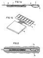
- FIG. 1A shows a system carrier 1 (a so-called lead frame) in a side sectional view. He has leads 2 on, of which only one in Figure 1A due to the representation is visible. With the system carrier 1 is an integrated Circuit 4 connected, which for protection with an envelope 9 is provided, which usually consists of a thermoset (Molded body). The casing 9 is only on one System carrier side 1.
- a system carrier 1 a so-called lead frame
- FIG. 1B shows the object from FIG. 1A in a perspective view Presentation.
- Sheath 9 is again shown and a plurality of leads 2, each having a contact area 3 for later external contacting of the integrated Switching from the outside of an injection molded housing that is still to be manufactured serve.
- the invention is based on a of leads 2 explained, where it goes without saying that all leads of system carrier 1 designed in the same way could be.
- Figure 1A shows that the lead 2 on its from the Envelope 9 protruding end is formed so that a approximately semi-circular spring element 6 is formed. This creates the resilient effect by pressure from below on the spring element 6 in the direction of the contact surface 3 (FIG. 1A). It is particularly favorable when the spring element 6 is nearby the contact surface 3 is arranged, as shown in Figure 1A. Because then one is transferred to the spring element 6 Force optimally on the contact surface 3.
- FIG. 1A shows that the lead 2 on its from the Envelope 9 protruding end is formed so that a approximately semi-circular spring element 6 is formed. This creates the resilient effect by pressure from below on the spring element 6 in the direction of the contact surface 3 (FIG. 1A). It is particularly favorable when the spring element 6 is nearby the contact surface 3 is arranged, as shown in Figure 1A. Because then one is transferred to the spring element 6 Force optimally on the contact surface 3.
- Below is a manufacturing process to explain the function of the spring element 6 for an injection molded housing for the integrated circuit
- Figure 2 shows the object of Figure 1A after it in a Injection mold 7a, 7b with an upper mold half 7a and a lower tool half 7b has been introduced.
- the two mold halves 7a, 7b of the injection mold not yet fully closed, so that on the spring element 6 no force is exerted yet.
- a possible manufacturing process of an injection molded housing is the so-called in-mold labeling, which is explained here.
- Figure 2 clearly shows that in this embodiment the invention advantageously the spring element 6 a projection over the thickness of the casing 9 has.
- the lower tool half 7b is already in contact with the spring element 6, but not yet the casing 9.
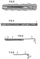
- Figure 3 shows the injection mold 7a, 7b after the final Put together. Due to the protrusion of the spring element 6 is this has been compressed during assembly. Through this caused spring force, the contact surface 3 against pressed an inner wall 8 of the upper tool half 7a. The following injection of a thermoplastic compound in the remaining cavity of the injection mold 7a, 7b is ensured by the spring element 6 that the Contact surface 3 on its top, that of a later external Contacting the integrated circuit is used, plan on the inner wall 8 rests, so that no plastic mass between the two can reach.
- Figure 4 shows the finished injection molded housing 5 after Removal of the injection mold 7a, 7b.
- Figure 4 is closed remove that the top of the contact surface 3 free of Is plastic.
- the spring force of the upset Spring element 6 of the lead 2 during the injection process held or fixed, so that a deformation of the Leads 2 is avoided during housing manufacture.
- Another advantage of the spring element 6 according to the invention is that by its shape anchoring the lead 2 in Injection molded housing 5 takes place. This means that even when it occurs bending or torsional loads on the injection molded housing 5 a detachment of the contact surface 3 from the housing 5 is avoided.
- the spring element 6, as in the embodiment explains part of the lead 2, so a possibly unwanted further contact at the bottom of the housing 5 via the spring element 6 by being present the lower decorative film 10 prevents the spring element 6 covers down.
- FIG. 5 shows another embodiment of the invention, in which the spring element 6 in turn is part of the lead 2 and is arranged in the immediate vicinity of the contact surface 3.
- the spring element is not semicircular but J-shaped educated. This is also easier to manufacture Embodiment of the invention will have the same advantages achieved as described above: prevention of flash formation at the top of the contact surface 3, prevention of bending of the lead 2 during the spraying process and anchoring of the lead 2 and thus the contact surface 3 in the finished Injection molded housing 5.
- the invention is particularly suitable for production very thin injection molded housing 5, especially for manufacturing of chip cards or similar cases.
- the invention enables the use of an injection mold without wear-sensitive hold-down pins. There will be holes avoided in the finished injection molded housing.
- Figure 6 shows a further embodiment of the invention. Only part of the system carrier 1 is shown, namely a part of the lead 2 with the contact surface 3 and the spring element 6, which is also part of this embodiment of the lead is 2.
- the spring element 6 is at the end of Leads 2 executed zigzag, which makes a particularly cheap springy behavior is effected.
- the end of the spring element 6 is again J-shaped for an additional Anchoring the lead 2 in the finished housing 5 too reach and a good contact surface for the injection mold 7a, 7b to offer.
Landscapes
- Engineering & Computer Science (AREA)
- Computer Hardware Design (AREA)
- Microelectronics & Electronic Packaging (AREA)
- Physics & Mathematics (AREA)
- General Physics & Mathematics (AREA)
- Theoretical Computer Science (AREA)
- Condensed Matter Physics & Semiconductors (AREA)
- Power Engineering (AREA)
- Injection Moulding Of Plastics Or The Like (AREA)
- Encapsulation Of And Coatings For Semiconductor Or Solid State Devices (AREA)
- Structures Or Materials For Encapsulating Or Coating Semiconductor Devices Or Solid State Devices (AREA)
- Manufacturing Of Electrical Connectors (AREA)
Abstract
Description
- Figuren 1A bis 4
- ein erstes Ausführungsbeispiel des erfindungsgemäßen Systemträgers und verschiedene Schritte der Gehäuseherstellung für eine mit diesem verbundene integrierte Schaltung.
- Figuren 5 und 6
- weitere Ausführungsbeispiele des erfindungsgemäßen Systemträgers.
Claims (7)
- Systemträger (1) für die Montage einer integrierten Schaltung (4) in einem Spritzgußgehäuse (5), der wenigstens einen Lead (2) aufweist, der eine Kontaktfläche (3) zur Kontaktierung der integrierten Schaltung (4) von außerhalb des Gehäuses (5) aufweist,
dadurch gekennzeichnet, dass
wenigstens einer der Leads (2) ein Federelement (6) aufweist, das so angeordnet ist, dass es beim Spritzgießen des Gehäuses (5) durch ein Spritzwerkzeug (7a, 7b) gestaucht wird, wodurch die Kontaktfläche (3) gegen eine Innenwand (8) des Spritzwerkzeugs (7a, 7b) gepresst wird. - Systemtrager nach Anspruch 1,
bei dem ein Ende des Leads (2) zum Federelement (6) ausgebildet ist. - Systemträger nach einem der vorstehenden Ansprüche,
bei dem das Federelement (6) hakenförmig ausgebildet ist, so daß nach Fertigstellung des Gehäuses (5) der Lead (2) darin verankert ist. - Systemträger nach Anspruch 3,
bei dem das Federelement (6) J-förmig ausgebildet ist. - Systemträger nach Anspruch 3,
bei dem das Federelement (6) halbkreisförmig ausgebildet ist. - Systemträger nach einem der vorstehenden Ansprüche,
bei dem das Federelement (6) wenigstens teilweise zickzackförmig ausgebildet ist. - Systemträger nach einem der vorstehenden Ansprüche,
bei dem das Federelement (6) so angeordnet ist, dass es durch Zusammenfügen zweier Teile des Spritzwerkzeugs (7a, 7b) gestaucht wird,
wobei das Federelement (6) einen Überstand gegenüber der Dikke des Gehäuses (5) aufweist.
Applications Claiming Priority (3)
| Application Number | Priority Date | Filing Date | Title |
|---|---|---|---|
| DE19625228 | 1996-06-24 | ||
| DE19625228A DE19625228C2 (de) | 1996-06-24 | 1996-06-24 | Systemträger für die Montage einer integrierten Schaltung in einem Spritzgußgehäuse |
| PCT/DE1997/001314 WO1997050056A1 (de) | 1996-06-24 | 1997-06-24 | Systemträger für die montage einer integrierten schaltung in einem spritzgussgehäuse |
Publications (2)
| Publication Number | Publication Date |
|---|---|
| EP0907928A1 EP0907928A1 (de) | 1999-04-14 |
| EP0907928B1 true EP0907928B1 (de) | 2001-12-12 |
Family
ID=7797849
Family Applications (1)
| Application Number | Title | Priority Date | Filing Date |
|---|---|---|---|
| EP97931650A Expired - Lifetime EP0907928B1 (de) | 1996-06-24 | 1997-06-24 | Systemträger für die montage einer integrierten schaltung in einem spritzgussgehäuse |
Country Status (7)
| Country | Link |
|---|---|
| US (1) | US6614100B1 (de) |
| EP (1) | EP0907928B1 (de) |
| JP (1) | JP3640676B2 (de) |
| KR (1) | KR100397081B1 (de) |
| CN (1) | CN1099703C (de) |
| DE (2) | DE19625228C2 (de) |
| WO (1) | WO1997050056A1 (de) |
Families Citing this family (14)
| Publication number | Priority date | Publication date | Assignee | Title |
|---|---|---|---|---|
| US6001672A (en) | 1997-02-25 | 1999-12-14 | Micron Technology, Inc. | Method for transfer molding encapsulation of a semiconductor die with attached heat sink |
| DE19800646C2 (de) * | 1998-01-09 | 2000-05-04 | Siemens Ag | Trägerelement für einen Halbleiterchip |
| EP0949582A1 (de) * | 1998-04-07 | 1999-10-13 | ESEC Management SA | Elektronikobjekt |
| EP0949583A1 (de) * | 1998-04-07 | 1999-10-13 | ESEC Management SA | Elektronikobjekt |
| TW508774B (en) * | 2000-09-15 | 2002-11-01 | Samsung Techwin Co Ltd | Lead frame, semiconductor package having the same, method of manufacturing semiconductor package, molding plates and molding machine for manufacturing semiconductor package |
| US7220615B2 (en) * | 2001-06-11 | 2007-05-22 | Micron Technology, Inc. | Alternative method used to package multimedia card by transfer molding |
| RU2004117773A (ru) * | 2001-11-23 | 2005-06-10 | Награид Са (Ch) | Способ изготовления модуля, содержащего, по меньшей мере, один электронный компонент |
| FR2895548B1 (fr) * | 2005-12-26 | 2008-03-21 | Oberthur Card Syst Sa | Procede de fabrication d'une carte a microcircuit, et carte a microcircuit associee |
| US7380721B2 (en) * | 2006-08-22 | 2008-06-03 | Honeywell International Inc. | Low-cost compact bar code sensor |
| US7768231B2 (en) * | 2006-09-18 | 2010-08-03 | Lg Chem, Ltd. | Battery pack |
| TWI331084B (en) * | 2008-05-12 | 2010-10-01 | Asustek Comp Inc | In-mold decoration device and manufacturing method thereof |
| EP2486624B1 (de) * | 2009-10-05 | 2015-03-25 | Cardiac Pacemakers, Inc. | Mehrbandantenne für eine implantierbare vorrichtung |
| DE102012204630A1 (de) | 2012-03-22 | 2013-09-26 | Robert Bosch Gmbh | Verfahren zur thermoplastischen Umspritzung und thermoplastische Umspritzung |
| JP6357371B2 (ja) * | 2014-07-09 | 2018-07-11 | 新光電気工業株式会社 | リードフレーム、半導体装置及びリードフレームの製造方法 |
Family Cites Families (37)
| Publication number | Priority date | Publication date | Assignee | Title |
|---|---|---|---|---|
| DE3051195C2 (de) * | 1980-08-05 | 1997-08-28 | Gao Ges Automation Org | Trägerelement zum Einbau in Ausweiskarten |
| FR2520541A1 (fr) * | 1982-01-22 | 1983-07-29 | Flonic Sa | Procede d'insertion d'un circuit integre dans une carte a memoire et carte obtenue suivant ce procede |
| US4801561A (en) * | 1984-07-05 | 1989-01-31 | National Semiconductor Corporation | Method for making a pre-testable semiconductor die package |
| JPS6394645A (ja) * | 1986-10-08 | 1988-04-25 | Mitsubishi Electric Corp | 電子装置 |
| FR2609821B1 (fr) * | 1987-01-16 | 1989-03-31 | Flonic Sa | Procede de realisation de cartes a memoire et cartes obtenues par la mise en oeuvre dudit procede |
| US5438481A (en) * | 1987-11-17 | 1995-08-01 | Advanced Interconnections Corporation | Molded-in lead frames |
| JPH01272142A (ja) * | 1988-04-25 | 1989-10-31 | Mitsubishi Electric Corp | 半導体集積回路用ソケット |
| US5030407A (en) * | 1988-04-28 | 1991-07-09 | Schlumberger Industries | Method of making cards having graphics elements thereon |
| US5244840A (en) * | 1989-05-23 | 1993-09-14 | Mitsubishi Denki Kabushiki Kaisha | Method for manufacturing an encapsulated IC card having a molded frame and a circuit board |
| JPH04284661A (ja) * | 1991-03-13 | 1992-10-09 | Toshiba Corp | 半導体装置 |
| CA2115553C (en) * | 1991-09-30 | 2002-08-20 | Deepak Keshav Pai | Plated compliant lead |
| JP3187106B2 (ja) * | 1991-12-27 | 2001-07-11 | ローム株式会社 | 電気回路素子のパッケージ構造 |
| US5155901A (en) * | 1991-12-30 | 1992-10-20 | Fierkens Richard H J | Integrated circuit lead frame positioner apparatus and method |
| US5328870A (en) * | 1992-01-17 | 1994-07-12 | Amkor Electronics, Inc. | Method for forming plastic molded package with heat sink for integrated circuit devices |
| US5446313A (en) * | 1992-05-25 | 1995-08-29 | Hitachi, Ltd. | Thin type semiconductor device and module structure using the device |
| US5715872A (en) * | 1992-10-14 | 1998-02-10 | Micron Technology, Inc. | Process and device for the shaping of leads of integrated circuits |
| JP3117828B2 (ja) * | 1992-12-28 | 2000-12-18 | ローム株式会社 | 合成樹脂封止型電子部品及びそのリード端子の曲げ加工方法 |
| JP2927660B2 (ja) * | 1993-01-25 | 1999-07-28 | シャープ株式会社 | 樹脂封止型半導体装置の製造方法 |
| US5474958A (en) * | 1993-05-04 | 1995-12-12 | Motorola, Inc. | Method for making semiconductor device having no die supporting surface |
| JP2560974B2 (ja) * | 1993-06-04 | 1996-12-04 | 日本電気株式会社 | 半導体装置 |
| US5555204A (en) * | 1993-06-29 | 1996-09-10 | Kabushiki Kaisha Toshiba | Non-volatile semiconductor memory device |
| JP2565091B2 (ja) * | 1993-07-01 | 1996-12-18 | 日本電気株式会社 | 半導体装置およびその製造方法 |
| US5767443A (en) * | 1993-07-10 | 1998-06-16 | Micron Technology, Inc. | Multi-die encapsulation device |
| US5420752A (en) * | 1993-08-18 | 1995-05-30 | Lsi Logic Corporation | GPT system for encapsulating an integrated circuit package |
| US5448824A (en) * | 1993-08-27 | 1995-09-12 | Delco Electronics Corporation | Method for forming a lead during molding of an electronic housing |
| JPH07230934A (ja) * | 1994-02-18 | 1995-08-29 | Rohm Co Ltd | 電子部品及びその基板実装構造 |
| KR950027550U (ko) * | 1994-03-07 | 1995-10-18 | 정의훈 | 클로즈 가이드(Cloth guide)의 경사안내로울러 좌. 우 이송장치 |
| US5494562A (en) * | 1994-06-27 | 1996-02-27 | Ciba Corning Diagnostics Corp. | Electrochemical sensors |
| SE514116C2 (sv) * | 1994-10-19 | 2001-01-08 | Ericsson Telefon Ab L M | Förfarande för framställning av en kapslad optokomponent, gjutform för kapsling av en optokomponent och tryckanordning för gjutform |
| US5945130A (en) * | 1994-11-15 | 1999-08-31 | Vlt Corporation | Apparatus for circuit encapsulation |
| US5682673A (en) * | 1995-04-17 | 1997-11-04 | Ipac, Inc. | Method for forming encapsulated IC packages |
| US6252302B1 (en) * | 1996-09-19 | 2001-06-26 | Warren M. Farnworth | Heat transfer material for an improved die edge contacting socket |
| JP3175609B2 (ja) * | 1996-11-19 | 2001-06-11 | 日本電気株式会社 | チップ型電子部品 |
| JP3011233B2 (ja) * | 1997-05-02 | 2000-02-21 | 日本電気株式会社 | 半導体パッケージ及びその半導体実装構造 |
| JPH1126678A (ja) * | 1997-06-30 | 1999-01-29 | Oki Electric Ind Co Ltd | 電子部品のリード構造 |
| US5869883A (en) * | 1997-09-26 | 1999-02-09 | Stanley Wang, President Pantronix Corp. | Packaging of semiconductor circuit in pre-molded plastic package |
| US6081424A (en) * | 1998-05-19 | 2000-06-27 | Chrysler Corporation | Mechanism for removing heat from electronic components |
-
1996
- 1996-06-24 DE DE19625228A patent/DE19625228C2/de not_active Expired - Fee Related
-
1997
- 1997-06-24 EP EP97931650A patent/EP0907928B1/de not_active Expired - Lifetime
- 1997-06-24 DE DE59705782T patent/DE59705782D1/de not_active Expired - Lifetime
- 1997-06-24 CN CN97194071A patent/CN1099703C/zh not_active Expired - Fee Related
- 1997-06-24 WO PCT/DE1997/001314 patent/WO1997050056A1/de not_active Ceased
- 1997-06-24 JP JP50210598A patent/JP3640676B2/ja not_active Expired - Fee Related
- 1997-06-24 KR KR10-1998-0708621A patent/KR100397081B1/ko not_active Expired - Fee Related
-
1998
- 1998-12-23 US US09/220,745 patent/US6614100B1/en not_active Expired - Lifetime
Also Published As
| Publication number | Publication date |
|---|---|
| US6614100B1 (en) | 2003-09-02 |
| DE19625228C2 (de) | 1998-05-14 |
| JP2000512782A (ja) | 2000-09-26 |
| DE19625228A1 (de) | 1998-01-02 |
| KR20000010656A (ko) | 2000-02-25 |
| DE59705782D1 (de) | 2002-01-24 |
| EP0907928A1 (de) | 1999-04-14 |
| JP3640676B2 (ja) | 2005-04-20 |
| WO1997050056A1 (de) | 1997-12-31 |
| KR100397081B1 (ko) | 2003-10-17 |
| CN1216623A (zh) | 1999-05-12 |
| CN1099703C (zh) | 2003-01-22 |
Similar Documents
| Publication | Publication Date | Title |
|---|---|---|
| EP0907928B1 (de) | Systemträger für die montage einer integrierten schaltung in einem spritzgussgehäuse | |
| EP0748486B1 (de) | Steckkarte für elektronische datenverarbeitungsgeräte und verfahren zu deren herstellung und montage | |
| EP0706214A2 (de) | Elektronikmodul und Chipkarte | |
| DE69205033T2 (de) | Elektrischer Steckverbinder mit Überbrückungen. | |
| DE19926300B4 (de) | Harzformverfahren zum Einsetzen eines Kontaktgebers, und mit dem Kontaktgeber versehener Motoranschluß | |
| EP1199913A2 (de) | Verfahren zur Herstellung von Leiterfolie-Trägergehäuse-Einheiten | |
| EP2122784A1 (de) | Sensoranordnung | |
| DE69113079T2 (de) | Leiterrahmen für Packungen von integrierten Leistungsanordnungen. | |
| DE19607786A1 (de) | Verbindungselement | |
| DE69126714T2 (de) | Teile einer Halbleitervorrichtung | |
| EP1743404A1 (de) | Verfahren zur herstellung eines kunststoffumspritzten stanzgitters und kunststoffumspritztes stanzgitter | |
| DE3212903A1 (de) | Verfahren zur herstellung von kunststoff-gehaeusen mit eingebautem waermeableiter fuer integrierte schaltungen und zur ausfuehrung des verfahrens geeignete kombination aus formwerkzeug und waermeableiter | |
| EP1451531B1 (de) | Fühler, vielzahl von fühlern und verfahren zur herstellung des fühlers | |
| DE3501391A1 (de) | Gehaeuse fuer ein elektrisches bauteil | |
| EP0502467B1 (de) | Halterung für eine Ringkerndrossel eines elektrischen Netzsteckers | |
| DE69210072T2 (de) | Elektrisches Verbindergehäuse | |
| DE69017929T2 (de) | Verbinderhalter. | |
| EP0507211A2 (de) | Vorrichtung zur Herstellung eines mit einer Isolationsschicht versehenen Kerns einer elektrischen Spule sowie mit der Vorrichtung herstellbarer Kern | |
| EP3996894B1 (de) | Gehäuse eines elektronikmoduls und dessen herstellung | |
| DE69204587T2 (de) | Elektrischer Kontaktstift für gedruckte Schaltungsplatten. | |
| DE3878574T2 (de) | Verbindungselemente. | |
| DE3239047A1 (de) | Elektromagnetisches relais | |
| DE3910717C2 (de) | Blattfederschalter mit einstückigem Gehäuse | |
| DE19902448A1 (de) | Trägerband | |
| DE4243575C2 (de) | Verfahren zum Herstellen einer Kabeleinführung in ein Gehäuse eines Sensors |
Legal Events
| Date | Code | Title | Description |
|---|---|---|---|
| PUAI | Public reference made under article 153(3) epc to a published international application that has entered the european phase |
Free format text: ORIGINAL CODE: 0009012 |
|
| 17P | Request for examination filed |
Effective date: 19981217 |
|
| AK | Designated contracting states |
Kind code of ref document: A1 Designated state(s): DE FR GB IT |
|
| 17Q | First examination report despatched |
Effective date: 20000524 |
|
| RAP1 | Party data changed (applicant data changed or rights of an application transferred) |
Owner name: INFINEON TECHNOLOGIES AG |
|
| GRAG | Despatch of communication of intention to grant |
Free format text: ORIGINAL CODE: EPIDOS AGRA |
|
| GRAG | Despatch of communication of intention to grant |
Free format text: ORIGINAL CODE: EPIDOS AGRA |
|
| GRAH | Despatch of communication of intention to grant a patent |
Free format text: ORIGINAL CODE: EPIDOS IGRA |
|
| GRAH | Despatch of communication of intention to grant a patent |
Free format text: ORIGINAL CODE: EPIDOS IGRA |
|
| GRAA | (expected) grant |
Free format text: ORIGINAL CODE: 0009210 |
|
| AK | Designated contracting states |
Kind code of ref document: B1 Designated state(s): DE FR GB IT |
|
| REG | Reference to a national code |
Ref country code: GB Ref legal event code: IF02 |
|
| REF | Corresponds to: |
Ref document number: 59705782 Country of ref document: DE Date of ref document: 20020124 |
|
| GBT | Gb: translation of ep patent filed (gb section 77(6)(a)/1977) |
Effective date: 20020227 |
|
| ET | Fr: translation filed | ||
| PLBE | No opposition filed within time limit |
Free format text: ORIGINAL CODE: 0009261 |
|
| STAA | Information on the status of an ep patent application or granted ep patent |
Free format text: STATUS: NO OPPOSITION FILED WITHIN TIME LIMIT |
|
| 26N | No opposition filed | ||
| PGFP | Annual fee paid to national office [announced via postgrant information from national office to epo] |
Ref country code: GB Payment date: 20070621 Year of fee payment: 11 |
|
| GBPC | Gb: european patent ceased through non-payment of renewal fee |
Effective date: 20080624 |
|
| PG25 | Lapsed in a contracting state [announced via postgrant information from national office to epo] |
Ref country code: GB Free format text: LAPSE BECAUSE OF NON-PAYMENT OF DUE FEES Effective date: 20080624 |
|
| PGFP | Annual fee paid to national office [announced via postgrant information from national office to epo] |
Ref country code: FR Payment date: 20110630 Year of fee payment: 15 |
|
| PGFP | Annual fee paid to national office [announced via postgrant information from national office to epo] |
Ref country code: IT Payment date: 20110625 Year of fee payment: 15 |
|
| PG25 | Lapsed in a contracting state [announced via postgrant information from national office to epo] |
Ref country code: IT Free format text: LAPSE BECAUSE OF NON-PAYMENT OF DUE FEES Effective date: 20120624 |
|
| REG | Reference to a national code |
Ref country code: FR Ref legal event code: ST Effective date: 20130228 |
|
| PG25 | Lapsed in a contracting state [announced via postgrant information from national office to epo] |
Ref country code: FR Free format text: LAPSE BECAUSE OF NON-PAYMENT OF DUE FEES Effective date: 20120702 |
|
| PGFP | Annual fee paid to national office [announced via postgrant information from national office to epo] |
Ref country code: DE Payment date: 20140723 Year of fee payment: 18 |
|
| REG | Reference to a national code |
Ref country code: DE Ref legal event code: R081 Ref document number: 59705782 Country of ref document: DE Owner name: POLARIS INNOVATIONS LTD., IE Free format text: FORMER OWNER: QIMONDA AG, 81739 MUENCHEN, DE Ref country code: DE Ref legal event code: R081 Ref document number: 59705782 Country of ref document: DE Owner name: INFINEON TECHNOLOGIES AG, DE Free format text: FORMER OWNER: QIMONDA AG, 81739 MUENCHEN, DE |
|
| REG | Reference to a national code |
Ref country code: DE Ref legal event code: R081 Ref document number: 59705782 Country of ref document: DE Owner name: POLARIS INNOVATIONS LTD., IE Free format text: FORMER OWNER: INFINEON TECHNOLOGIES AG, 85579 NEUBIBERG, DE |
|
| REG | Reference to a national code |
Ref country code: DE Ref legal event code: R119 Ref document number: 59705782 Country of ref document: DE |
|
| PG25 | Lapsed in a contracting state [announced via postgrant information from national office to epo] |
Ref country code: DE Free format text: LAPSE BECAUSE OF NON-PAYMENT OF DUE FEES Effective date: 20160101 |