EP0904559B1 - Dispositif de balayage a laser pulse a longueur d'onde courte - Google Patents
Dispositif de balayage a laser pulse a longueur d'onde courte Download PDFInfo
- Publication number
- EP0904559B1 EP0904559B1 EP97953077A EP97953077A EP0904559B1 EP 0904559 B1 EP0904559 B1 EP 0904559B1 EP 97953077 A EP97953077 A EP 97953077A EP 97953077 A EP97953077 A EP 97953077A EP 0904559 B1 EP0904559 B1 EP 0904559B1
- Authority
- EP
- European Patent Office
- Prior art keywords
- laser
- pulsed
- medium
- modulated
- pattern generator
- Prior art date
- Legal status (The legal status is an assumption and is not a legal conclusion. Google has not performed a legal analysis and makes no representation as to the accuracy of the status listed.)
- Expired - Lifetime
Links
Images




Classifications
-
- H—ELECTRICITY
- H04—ELECTRIC COMMUNICATION TECHNIQUE
- H04N—PICTORIAL COMMUNICATION, e.g. TELEVISION
- H04N1/00—Scanning, transmission or reproduction of documents or the like, e.g. facsimile transmission; Details thereof
- H04N1/40—Picture signal circuits
- H04N1/40025—Circuits exciting or modulating particular heads for reproducing continuous tone value scales
- H04N1/40037—Circuits exciting or modulating particular heads for reproducing continuous tone value scales the reproducing element being a laser
-
- G—PHYSICS
- G02—OPTICS
- G02B—OPTICAL ELEMENTS, SYSTEMS OR APPARATUS
- G02B26/00—Optical devices or arrangements for the control of light using movable or deformable optical elements
- G02B26/08—Optical devices or arrangements for the control of light using movable or deformable optical elements for controlling the direction of light
- G02B26/10—Scanning systems
-
- B—PERFORMING OPERATIONS; TRANSPORTING
- B23—MACHINE TOOLS; METAL-WORKING NOT OTHERWISE PROVIDED FOR
- B23K—SOLDERING OR UNSOLDERING; WELDING; CLADDING OR PLATING BY SOLDERING OR WELDING; CUTTING BY APPLYING HEAT LOCALLY, e.g. FLAME CUTTING; WORKING BY LASER BEAM
- B23K26/00—Working by laser beam, e.g. welding, cutting or boring
- B23K26/02—Positioning or observing the workpiece, e.g. with respect to the point of impact; Aligning, aiming or focusing the laser beam
- B23K26/03—Observing, e.g. monitoring, the workpiece
- B23K26/032—Observing, e.g. monitoring, the workpiece using optical means
-
- B—PERFORMING OPERATIONS; TRANSPORTING
- B23—MACHINE TOOLS; METAL-WORKING NOT OTHERWISE PROVIDED FOR
- B23K—SOLDERING OR UNSOLDERING; WELDING; CLADDING OR PLATING BY SOLDERING OR WELDING; CUTTING BY APPLYING HEAT LOCALLY, e.g. FLAME CUTTING; WORKING BY LASER BEAM
- B23K26/00—Working by laser beam, e.g. welding, cutting or boring
- B23K26/02—Positioning or observing the workpiece, e.g. with respect to the point of impact; Aligning, aiming or focusing the laser beam
- B23K26/06—Shaping the laser beam, e.g. by masks or multi-focusing
-
- B—PERFORMING OPERATIONS; TRANSPORTING
- B23—MACHINE TOOLS; METAL-WORKING NOT OTHERWISE PROVIDED FOR
- B23K—SOLDERING OR UNSOLDERING; WELDING; CLADDING OR PLATING BY SOLDERING OR WELDING; CUTTING BY APPLYING HEAT LOCALLY, e.g. FLAME CUTTING; WORKING BY LASER BEAM
- B23K26/00—Working by laser beam, e.g. welding, cutting or boring
- B23K26/02—Positioning or observing the workpiece, e.g. with respect to the point of impact; Aligning, aiming or focusing the laser beam
- B23K26/06—Shaping the laser beam, e.g. by masks or multi-focusing
- B23K26/064—Shaping the laser beam, e.g. by masks or multi-focusing by means of optical elements, e.g. lenses, mirrors or prisms
-
- B—PERFORMING OPERATIONS; TRANSPORTING
- B23—MACHINE TOOLS; METAL-WORKING NOT OTHERWISE PROVIDED FOR
- B23K—SOLDERING OR UNSOLDERING; WELDING; CLADDING OR PLATING BY SOLDERING OR WELDING; CUTTING BY APPLYING HEAT LOCALLY, e.g. FLAME CUTTING; WORKING BY LASER BEAM
- B23K26/00—Working by laser beam, e.g. welding, cutting or boring
- B23K26/02—Positioning or observing the workpiece, e.g. with respect to the point of impact; Aligning, aiming or focusing the laser beam
- B23K26/06—Shaping the laser beam, e.g. by masks or multi-focusing
- B23K26/064—Shaping the laser beam, e.g. by masks or multi-focusing by means of optical elements, e.g. lenses, mirrors or prisms
- B23K26/0643—Shaping the laser beam, e.g. by masks or multi-focusing by means of optical elements, e.g. lenses, mirrors or prisms comprising mirrors
-
- B—PERFORMING OPERATIONS; TRANSPORTING
- B23—MACHINE TOOLS; METAL-WORKING NOT OTHERWISE PROVIDED FOR
- B23K—SOLDERING OR UNSOLDERING; WELDING; CLADDING OR PLATING BY SOLDERING OR WELDING; CUTTING BY APPLYING HEAT LOCALLY, e.g. FLAME CUTTING; WORKING BY LASER BEAM
- B23K26/00—Working by laser beam, e.g. welding, cutting or boring
- B23K26/02—Positioning or observing the workpiece, e.g. with respect to the point of impact; Aligning, aiming or focusing the laser beam
- B23K26/06—Shaping the laser beam, e.g. by masks or multi-focusing
- B23K26/064—Shaping the laser beam, e.g. by masks or multi-focusing by means of optical elements, e.g. lenses, mirrors or prisms
- B23K26/0648—Shaping the laser beam, e.g. by masks or multi-focusing by means of optical elements, e.g. lenses, mirrors or prisms comprising lenses
-
- B—PERFORMING OPERATIONS; TRANSPORTING
- B23—MACHINE TOOLS; METAL-WORKING NOT OTHERWISE PROVIDED FOR
- B23K—SOLDERING OR UNSOLDERING; WELDING; CLADDING OR PLATING BY SOLDERING OR WELDING; CUTTING BY APPLYING HEAT LOCALLY, e.g. FLAME CUTTING; WORKING BY LASER BEAM
- B23K26/00—Working by laser beam, e.g. welding, cutting or boring
- B23K26/02—Positioning or observing the workpiece, e.g. with respect to the point of impact; Aligning, aiming or focusing the laser beam
- B23K26/06—Shaping the laser beam, e.g. by masks or multi-focusing
- B23K26/0665—Shaping the laser beam, e.g. by masks or multi-focusing by beam condensation on the workpiece, e.g. for focusing
-
- B—PERFORMING OPERATIONS; TRANSPORTING
- B23—MACHINE TOOLS; METAL-WORKING NOT OTHERWISE PROVIDED FOR
- B23K—SOLDERING OR UNSOLDERING; WELDING; CLADDING OR PLATING BY SOLDERING OR WELDING; CUTTING BY APPLYING HEAT LOCALLY, e.g. FLAME CUTTING; WORKING BY LASER BEAM
- B23K26/00—Working by laser beam, e.g. welding, cutting or boring
- B23K26/08—Devices involving relative movement between laser beam and workpiece
-
- B—PERFORMING OPERATIONS; TRANSPORTING
- B23—MACHINE TOOLS; METAL-WORKING NOT OTHERWISE PROVIDED FOR
- B23K—SOLDERING OR UNSOLDERING; WELDING; CLADDING OR PLATING BY SOLDERING OR WELDING; CUTTING BY APPLYING HEAT LOCALLY, e.g. FLAME CUTTING; WORKING BY LASER BEAM
- B23K26/00—Working by laser beam, e.g. welding, cutting or boring
- B23K26/08—Devices involving relative movement between laser beam and workpiece
- B23K26/082—Scanning systems, i.e. devices involving movement of the laser beam relative to the laser head
-
- B—PERFORMING OPERATIONS; TRANSPORTING
- B23—MACHINE TOOLS; METAL-WORKING NOT OTHERWISE PROVIDED FOR
- B23K—SOLDERING OR UNSOLDERING; WELDING; CLADDING OR PLATING BY SOLDERING OR WELDING; CUTTING BY APPLYING HEAT LOCALLY, e.g. FLAME CUTTING; WORKING BY LASER BEAM
- B23K26/00—Working by laser beam, e.g. welding, cutting or boring
- B23K26/08—Devices involving relative movement between laser beam and workpiece
- B23K26/082—Scanning systems, i.e. devices involving movement of the laser beam relative to the laser head
- B23K26/0821—Scanning systems, i.e. devices involving movement of the laser beam relative to the laser head using multifaceted mirrors, e.g. polygonal mirror
-
- G—PHYSICS
- G02—OPTICS
- G02B—OPTICAL ELEMENTS, SYSTEMS OR APPARATUS
- G02B26/00—Optical devices or arrangements for the control of light using movable or deformable optical elements
- G02B26/08—Optical devices or arrangements for the control of light using movable or deformable optical elements for controlling the direction of light
- G02B26/10—Scanning systems
- G02B26/12—Scanning systems using multifaceted mirrors
-
- G—PHYSICS
- G03—PHOTOGRAPHY; CINEMATOGRAPHY; ANALOGOUS TECHNIQUES USING WAVES OTHER THAN OPTICAL WAVES; ELECTROGRAPHY; HOLOGRAPHY
- G03F—PHOTOMECHANICAL PRODUCTION OF TEXTURED OR PATTERNED SURFACES, e.g. FOR PRINTING, FOR PROCESSING OF SEMICONDUCTOR DEVICES; MATERIALS THEREFOR; ORIGINALS THEREFOR; APPARATUS SPECIALLY ADAPTED THEREFOR
- G03F7/00—Photomechanical, e.g. photolithographic, production of textured or patterned surfaces, e.g. printing surfaces; Materials therefor, e.g. comprising photoresists; Apparatus specially adapted therefor
- G03F7/70—Microphotolithographic exposure; Apparatus therefor
- G03F7/70383—Direct write, i.e. pattern is written directly without the use of a mask by one or multiple beams
- G03F7/704—Scanned exposure beam, e.g. raster-, rotary- and vector scanning
-
- H—ELECTRICITY
- H10—SEMICONDUCTOR DEVICES; ELECTRIC SOLID-STATE DEVICES NOT OTHERWISE PROVIDED FOR
- H10P—GENERIC PROCESSES OR APPARATUS FOR THE MANUFACTURE OR TREATMENT OF DEVICES COVERED BY CLASS H10
- H10P76/00—Manufacture or treatment of masks on semiconductor bodies, e.g. by lithography or photolithography
- H10P76/20—Manufacture or treatment of masks on semiconductor bodies, e.g. by lithography or photolithography of masks comprising organic materials
- H10P76/204—Manufacture or treatment of masks on semiconductor bodies, e.g. by lithography or photolithography of masks comprising organic materials of organic photoresist masks
- H10P76/2041—Photolithographic processes
- H10P76/2042—Photolithographic processes using lasers
Definitions
- This invention relates to laser scanners and especially to a laser scanner using short wavelength laser radiation.
- Photolithography is commonly employed to produce repeatable patterns on devices such as integrated circuits, integrated circuit masks, flat panel displays, and printed circuit boards.
- a conventional photolithography process coats a workpiece with a layer of photoresist and illuminates selected regions of the photoresist with light that changes the properties of the illuminated regions.
- the photoresist layer is then developed and either the illuminated regions or not-illuminated regions (depending on the type of photoresist) are removed to leave a patterned layer covering portions of the workpiece.
- the workpiece is then subjected to a process such as etching where the covered portions of the workpiece are protected from the process.
- a laser scanner is a photolithographic device which scans one or more focused and spatially modulated laser beams in a series of scan lines covering a layer being patterned. Whether a laser scanner illuminates a region depends on the laser beam's intensity as the beam scans passes the region. The precision of a laser scanner in selecting regions illuminated depends on the accuracy of modulation of the laser beam, the sharpness of the focus of the laser beam, the precision with which the laser beam moves across the layer being patterned, and synchronization between modulation and movement of the laser beam.
- a typical scanner includes a laser, a modulator, scan optics, and a precision stage.
- the laser generates a collimated light beam which in a multi-beam system is split into an array of separate collimated sub-beams.
- the laser beam is ultraviolet light of wavelength e.g. 363.8 nm (nanometers), or 325 nm.
- Modulation of the array of beam changes the intensities of the individual sub-beams independently, typically turning sub-beams on and off; grayscale (intensity) control can also be employed.
- Scan optics including a rotating reflective polygon or other scanning device and a scan lens, forms an image of the beam or array and sweeps that image across a scan line in an image plane of the scan optics onto the surface of the workpiece to be exposed, which is held on an X-Y stage.
- the stage precisely moves the workpiece approximately perpendicular to the scan line direction. Movement of the workpiece can be continuous during scanning or may only occur during the dead time between scan lines.
- sub-beams in the beam are turned on and off to control which regions within the scan line at the surface of the device are illuminated.
- a typical application of such laser scanners is, as described above, for photolithography.
- Certain semiconductor photolithography applications require formation of very small size features.
- Commercially available photolithography equipment has a numerical aperture of the lens system of less than 0.80, approximately the limit of what is practical with light (ultraviolet) wavelengths. Remaining avenues for resolution improvement require use of shorter wavelengths.
- typical wavelengths used in the prior art are in the 350 nm region. It is not possible simply to obtain a commercially available compact continuous wave laser capable of efficiently operating at shorter wavelengths with powers above approximately 1 Watt.
- Pulsed solid-state lasers have been demonstrated with powers greater than 1 Watt. Hence, there is a need for photolithography equipment capable of operating with a pulsed short wavelength source for forming very small size features, i.e. features of 300 nm or less in size.
- Laser pattern generation e.g. for mask making or for direct writing of features for instance on semiconductor wafers, to form devices having a feature size of 300 nm or less requires high resolution imaging, only provided by short wavelength radiation, i.e. about 250 nm or less. There is direct ratio between laser wavelength and feature size; it is difficult to fabricate a feature size substantially smaller than the wavelength of the exposure radiation.
- a laser pattern generator using a pulsed laser operating at e.g. 355 nm or less instead of a conventional continuous wave laser, allows use of short wavelength laser radiation and hence fabrication of small feature sizes.
- the present laser pattern generator employs in one embodiment a laser outputting pulsed coherent light at a wavelength of e.g. 263 nm.
- This laser is pulsed at high frequency, providing a stream of laser pulses rather than a continuous output beam.
- the present laser pattern generator may operate in a synchronous mode, where the pulse rate of the laser is synchronous to the beam placement on the writing grid, i.e. the data which is used to operate the modulator is synchronous to the laser beam pulse rate. In this case, the modulator rise time can be much shorter than the laser pulse.
- Another type of laser pattern generator in accordance with this invention is an asynchronous type, in which the pulse rate of the laser is at least as fast as the pixel rate of the data used for writing the pattern, and the phase of the pulse rate of the laser is independent of the phase of the external modulator.
- the modulation rise time in this case is comparable to or greater than the pixel period of the data being written.
- a mode locked laser is used in an otherwise conventional laser scanner of the type commercially available.
- the data defining the pattern to be written i.e. on, off or gray level data
- the pulse rate is comparable to or faster than the modulation rate and hence not synchronous to the data defining the pattern.
- the laser In order to have an efficient operating laser pattern generator, the laser typically has a pulse rate greater than one MHz in either embodiment. Moreover, the spot size to pixel grid separation is large enough to ensure a smooth image intensity.
- the laser itself is a mode-locked solid state laser outputting light at e.g. 263 nm.
- Commercially available laser pattern and generators already operate in the ultraviolet. Hence, their optics which are optimized for somewhat higher e.g. 350 nm wavelengths, are readily reconfigured by routine optical engineering to deal with the shorter present 263 nm wavelength.
- the present invention is not limited to a 263 nm laser and is applicable to longer wavelengths and also to shorter wavelengths, to the extent that suitable laser sources are available operating at shorter wavelengths.
- the present invention is directed to the use of a pulsed laser source in a laser pattern generator without limitation to the wavelength of the laser radiation.
- the invention is defined by the subject-matter of claims 1-19.
- Fig. 1 is a simplified diagram of a laser pattern generator in accordance with this invention.
- This laser pattern generator in terms of most of its components, is conventional and generally is of the type described in the above-referenced U.S. Patents, and is also similar to a variety of commercially available laser pattern generators as used for photolithography.
- this laser pattern generator includes, instead of a conventional CW laser, a pulsed laser 40, which emits a series of laser pulses indicated as laser beam 42 which is pulsed at a relatively high frequency, i.e. 100 MHz with a range of typically 1 to 300 MHz.
- a pulsed laser 40 which emits a series of laser pulses indicated as laser beam 42 which is pulsed at a relatively high frequency, i.e. 100 MHz with a range of typically 1 to 300 MHz.
- Such a laser can be constructed from a mode-locked Nd:YLF laser driving an external cavity that is resonant for second harmonic radiation. This approach has been described, for instance, in S.C. Tidwell, J.F. Seamans, D.D. Lowenthal, G. Matone and G.
- the pulsed laser beam 42 is coupled to the optical input port of an acousto-optic modulator 46, which also has an electrical port receiving a Data signal as shown.
- This Data signal represents the pattern to be written.
- the laser beam 42 is split into a number of sub-beams and the modulator 46 individually modulates each of the sub-beams, as is well known in this field.
- the modulated beam output from modulator 46 is incident upon the reflective facets of a conventional rotating polygon 48 of the type well known in this field. This is the actual scanning device and is part of the scanning optics. Other types of scanners may also be used. For instance, see “Highly Accurate Pattern Generation Using Acousto-Optical Deflection" Sanstrom et al., SPIE Vol.
- Optical/ Laser Microlithography (1991), pp. 629 and following, which discloses a laser reticle writer using acousto-optical deflection for scanning.
- An acousto-optical scanner hence is substitutable for a polygon-type scanner and was found to be faster at short scans.
- Fig. 1 shows the rotating polygon scanning device 48, an acousto-optical deflection device or equivalent can be substituted.
- the scanning laser beam reflected from the facets of rotating polygon 48, passes through the scan lens 52 which typically includes refractive (and sometimes reflective) optics which focus the beam on the upper surface of workpiece 54, which in turn is held on stage 58.
- the workpiece is e.g. a reticle (a transparent substrate on which is formed a layer e.g. of metal to be patterned and over which is also formed a photoresist layer to be exposed by the scanning beam).
- a reticle a transparent substrate on which is formed a layer e.g. of metal to be patterned and over which is also formed a photoresist layer to be exposed by the scanning beam.
- Commercially available photo-resists are exposed by an approximately 250 nm wavelength laser beam. Examples of such photo-resists are APEX-E and UV-III from Shipley.
- the modulator 46 is optimized for the 250 nm wavelength region in terms of transducer geometry and acoustic coupling.
- the refractive elements of the scan lens 52 using conventional fused silica and if necessary, calcium fluoride lens elements, are optimized for the particular incident wavelength. Such modifications are well within the skill of one of ordinary skill in the art.
- a typical optical output power level of laser 40 is 1 Watt.
- the apparatus of Fig. 1 takes one of at least two embodiments.
- the pixels i.e. the data applied to the electrical port of modulator 46
- the pulse rate of the laser is a fixed frequency dependent on the actual laser cavity design and materials.
- the laser pulses in one embodiment are 50 picoseconds long and have a period of e.g. 13 nanoseconds (ns). (The pulse rate is 50 to 100 MHz.) Of course, this is only exemplary and other wavelengths are possible for the laser as are other pulse lengths and periods (pulse frequencies).
- Fig. 2 shows an example of a pattern scanned by such a synchronous mode laser scanner.
- the edge position of the feature being written (shown by the circles which are intended to be exposed beam spots or pixels) represents the feature edge position determined by a fixed writing grid and the modulator state, i.e. on, off, grayscale, at the edge pixels. Grayscale (variations in image intensity between on and off) may also be used.
- the individual spots, i.e. exposed pixels are formed in a sequence by laser pulses on the fixed writing grid.
- the polygon scan axis is the horizontal axis and the stage axis of movement is the vertical axis.
- the pixels being on or off represent an edge of the feature, shown by line A.
- Fig. 3 shows writing in the (second) asynchronous mode embodiment.
- the individual pixel spots are not aligned to the writing grid, but are turned off gradually by the modulator 46, in order to achieve the writing pattern shown in Fig. 2.
- the modulator intensity profile determines the feature edge position, shown by line B.
- This embodiment also can be used in conjunction with grayscale, but again grayscale is not necessary.
- the laser pulse rate is e.g. 200 MHz.
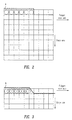
- Figs. 4A and 4B show, respectively, the transmitted intensity versus scan position and the dose versus scan position for the asynchronous mode second embodiment.
- the edge location of the deposited dose on the workpiece is a function of the modulation wave form position and not the phase of the pulse train. Hence, this writing method is "phase independent".
- Fig. 5 shows a block diagram of a laser scanner in the (first) synchronous mode embodiment.
- this laser scanner is similar to those known in the prior art and referred to above, with the addition of an acousto-optic deflector and associated optics for performing the synchronizing, the accompanying signal processing electronics, and the substitution of a pulsed laser for a nonpulsed (continuous operating) laser. Therefore operation of the apparatus of Fig. 5 is easily understood by one of ordinary skill in the art. Hence the emphasis in the following description is on the novel elements, rather than on the conventional aspects of this apparatus.
- the apparatus of Fig. 5 has many common elements with that of Fig. 5 of above-referenced U.S. Patent No. 5,386,221.
- the apparatus of Fig. 5 has many common elements with that of Fig. 5 of above-referenced U.S. Patent No. 5,386,221.
- the apparatus of Fig. 5 has many common elements with that of Fig. 5 of above-referenced U.S. Patent No
- a multi-beam apparatus e.g. having 32 laser sub-beams in one version to create a "brush" which scans the workpiece (reticle or wafer) by a rotating polygonal mirror.
- Each beam of the brush is modulated by a multi-channel acousto-optical modulator (AOM).
- AOM acousto-optical modulator
- the electrical signals coupled to these channels determine the specific patterns to be generated. This electrical signals are created by a rasterizer.
- Pulsed laser 100 provides a laser beam in the ultraviolet (approximately 250 nm wavelength, e.g. 263 and/or 266 nm) as described above.
- the laser beam is attenuated by attenuator 102 to adjust the power range to the resist exposure requirements and steered by a beam steering apparatus 104, which reduces the need to perform manual alignment of the source laser beam.
- the stigmator 108 through which the laser beam next passes, insures that the beam is circular by correcting for any elipticity and other astigmatic problems.
- the corrected beam is then split into e.g. 32 individual sub-beams by beam splitter 110.
- the plurality of sub-beams is collectively referred to as the brush.
- the brush passes through a brush module optics 114 (a relay lens) to re-image and shrink the beams.
- the brush then enters the acousto-optical modulator (AOM) 116.
- the AOM modulates the intensity of a laser beam to a level corresponding to one of the grayscale levels, for instance provided by the grayscale rasterization as shown.
- Electrical signals to drive the AOM are generated as shown beginning with the data which is the geometric descriptions 122 of the patterns (features) to be written. These come for instance from a computer or other source and define the actual patterns which are to be written on the medium, for instance portions of an integrated circuit.
- multichannel data in some embodiments including grayscale rasterization, drives the multi-channel AOM 116 (having one channel for each sub-beam).
- the modulated brush then passes through a relay optics 130 which causes the sub-beams to converge on a spot on a steering mirror 132.
- the steering mirror 132 provides for small corrections to the placement of the brush and the stripe axis at the final image plane.
- the steering mirror 132 alters the angle at which the brush impinges on the polygon mirror 148 in the stripe direction.
- a stripe correction error factor is also applied to adjust the steering mirror 132.
- acousto-optic deflector (AOD) 140 on which the afocal spot on the steering mirror is reimaged by optics 136 and which in turn directs the brush into optics 142.
- Optics 142 further reimages the afocal spot inside the AOD onto the rotating polygon.
- the zero-order beam stop is not shown for clarity.
- Acousto-optic deflector 140 provides the synchronization as described above and in further detail below.
- Such acousto-optic deflectors are available, for instance, from Newport EOS.
- the optics 136 and 142 are simple relay lenses, i.e. focussing and defocussing optics, and hence not described in any further detail.
- the optics 136 and 142 together perform the function of brush magnification adjustment to adjust the size of the array of sub-beams, i.e. so that they are enlarged and moved farther apart or made smaller and move closer together.
- the brush is then directed onto the facets of the rotating polygon mirror 148 which has e.g. 24 facets and causes the brush to scan the workpiece along the scan axis.
- the polygon mirror 148 rotates at a constant rate of 20,000 rpm.
- the once per facet (OPF) sensor 152 performs polygon synchronization and stage control, as described in above-referenced Patent No. 5,386,221, and includes the laser light source 152 and the pickup 154.
- the brush reflected from the rotating polygon mirror 148 passes through an f-theta lens assembly 160 which creates an enlarged intermediate image plane, e.g. 33 times the size of the image plane.
- the reduction lens 186 is located at the other end of the enlarged image plane.
- the brush exiting the reduction lens 186 is made up of the beams that actually scan the workpiece, illustrated here as a reticle (semiconductor mask) 196.
- a beam splitter 164 disposed within the enlarged intermediate image plane is used for two subsystems.
- One subsystem is an alignment system 178 which captures images of alignment marks on the workpiece using a non-exposing wavelength.
- the second subsystem is a facet detect photo multiplier tube (PMT) 168.
- the facet detect PMT 168 is used for the timing of data for each of the facets of the rotating polygon mirror 148. This allows synchronization of the provision of information from the data path 124 to (1) the AOM 116 and (2) to the rotation of the rotating polygon mirror 148.
- the alignment system 178 is used to detect the position of patterns previously written on the workpiece, so that the pattern to be written can be accurately aligned to the previously written pattern.
- the pattern alignment system also includes a calibration photo multiplier tube (PMT) 182 providing pattern acquisition data for purposes of machine set-up and adjustment.
- PMT calibration photo multiplier tube
- LMS laser measurement system
- Focus sensor (nose piece) 192 is as described in U.S. Patent No. 5,087,927, issued February 11, 1992 to Tim Thomas et al., entitled "On-axis Air Gage Focus System.”
- the reticle 196 is located on a stage (not shown) which includes a stage mirror 200.
- the LMS includes a laser 206 with beam splitters 208, 212, 214 providing beams to measure the relative position of the stage to the reduction lens.
- the pulsed laser 100 operates at a fixed pulse frequency and pulse length which cannot readily be varied, being inherent in the construction of the laser. Therefore in accordance with the invention the optical system has been modified by provision of optics 136 and 142 to provide an additional afocal point between the steering mirror 132 and rotating polygon 148, at the location of the acousto-optic deflector 140.
- the AOD 140 operates due to a change in its drive frequency, i.e.
- the electrical signal provided to its electrical port to cause a small angle change to the laser brush when it reaches rotating polygon 148, which in turn corrects a small angle change to the output of the scanner so it can be used to adjust the scan position of the brush to position the laser pulses at predetermined grid locations at the writing surface on reticle 196. This is required to compensate for pointing errors between the polygon 148 facets and to correct for scan position errors in the motion of the stage supporting reticle 196 by timing corrections of the data.
- the position of the pulses is determined by a timing grating 210 located at the start of the scan at the intermediate image plane provided by the beam splitting cube 164. Hence this synchronization occurs once per scan.
- Grating 210 has a period of twice the distance between laser pulses.
- One of the 32 beams is turned on by the modulator 116 for a small portion of the scan line at the start of each scan.
- the radiation transmitted through the beam splitting cube 164 is blocked by a beam stop (not shown) just as in conventional facet detection.
- the radiation reflected from the hypotenuse of the beam splitting cube 164 is focused on the grating 210.
- Fig. 6A shows detail of Fig. 5.
- PMT detector 168 is located behind the grating 210 to generate an electronic signal proportional to the amount of light transmitted through the grating for each laser pulse and provides this signal to servo control 170 which controls AOD driver 218 (shown in Fig. 5 as part of AOD 140).
- Grating 210 includes in one embodiment a grating part for pulse synchronization and a slit for facet detection; however the grating and slit do not have to be on the same structure.
- the servo control electronics 170 driving the AOD 140 develops two time averaged signals from respectively the even and odd numbered pulses.
- the error signal of the servo is the difference between these two signals compared with the timing correction signal.
- the error signal causes a frequency change in the AOD driver electronics 218 which advances or retards the scanned signal (as shown in Fig. 6B) accordingly until a null condition is reached. At this point the frequency of the AOD 140 is locked until the facet detect signal is received.
- This signal for the start of data can be obtained from a slit located after an opaque region of the grating 210 and an appropriate grating delay.
- Fig. 7A shows the beams (the curves) incident on grating 210, with the resulting detected odd/even signal strengths A, B at detector 168 being shown graphically in Fig. 7B.
- Fig. 7C shows the beams, shifted in phase by 180°, incident on grating 210 and the resulting detector 168 signal strengths A/B in Fig. 7D; when signals A and B are equal (Fig. 7D), the desired phase adjustment has been accomplished to achieve synchronization for no timing correction.
- a non-zero timing correction may be introduced to set the appropriate phase after facet detect.
- the signal from a pulsed spot strobed on the facet detect slit in grating 210 together with the phase adjustment from the grating servo give a signal representing the true position of the laser beam, independent of the timing of the laser beam pulses.
- An appropriate data delay is introduced along with the phase setting to place the pulsed beam at the correct location on the workpiece at the correct time. (This is used in the synchronous embodiment.)
- Fig. 8 shows a detailed block diagram of servo control electronics 170 (for the synchronous embodiment).
- PMT (photomultiplier tube) 168 provides its output signal to a preamplifier 224 which drives a 38.5 MHz bandpass filter 228, the output signal of which is coupled to a synchronous demodulator 230.
- the other input port of synchronous demodulator 230 is coupled to a second 38.5 MHz BDF 236, driven in turn by the clock pulse 242 from laser 100 divided by two by e.g. flip-flop 240.
- Demodulator 230 drives 1 MHz low pass filter 246 which outputs an error signal to AOD driver 218 of Fig. 6A.
- N N D
- N D the number of spots of deflection required to shift by one writing grid unit plus some margin, about 5.
- N A the number of spots in the array of scanned spots or "brush" of the system, e.g. 102 spots in one version.
- the reason for this additional term is to allow for meeting the Bragg angle tolerance on the input to the AOD.
- the configuration of the AOD 140 and the array of beams is shown in Fig. 6B.
- N A (4/ ⁇ )D A /d 1/e2 , where D A is the length of the array inside the multi-transducer AOM 116 and d 1/e2 is the 1/e 2 diameter of each of the beams inside the AOM 116. (The factor 4/ ⁇ comes about from measuring a resolved spot at the 40% intensity point rather than the 1/e 2 intensity'point.)
- the total number of resolved spots, N determines the AOD 140 configuration and the preparation of the input beams. In particular the input beam diameter must be made big enough, and therefore the angular spread of the array small enough, so the total angular input plus any deflection angle falls within the Bragg angle acceptance tolerance. An N of 110 is sufficient.
- t N/ ⁇ F.
- AOD devices are commercially available with 110 MHz bandwidth giving a transit time of 1 ⁇ s.
- a typical facet period of polygon 148 is 125 ⁇ s.
- a laser pulse period of e.g. 10 to 20 ns gives 50 to 100 samples per transit time, adequate to prepare an averaged error signal from the grating 210. Devoting 10 ⁇ s of the scan period for grating synchronization allows 10 servo loop time constants for equilibrium to be established.
- Fig. 9 shows a detailed block diagram of the asynchronous (second) mode embodiment. Most of the elements are identical to those of Fig. 5 and are identically labeled. In one embodiment, magnification adjustment optics (not shown) are located intermediate steering mirror 132 and polygon 148. There is no AOD or AOD driver or AOD grating; hence filter block 171 differs from and is simpler than servo block 170 of Fig. 5 and is for purposes of facet detection only, as described below.
- the present inventors have found that two challenges of the asynchronous embodiment are first keeping the edge location of a printed feature invariant to changes in laser pulse phase and second, detecting the scanned beam at facet detect in such a way that its measured position is also independent of the laser pulse phase.
- a pulsed laser scanning system scans a pulsed Gaussian shaped laser beam across the writing surface. For pulses that are short compared to the pixel dwell time, the pulses can be treated as infinitesimally short.
- This writing beam is turned on or off by the acousto-optic modulator 116 (AOM). As the sound wave inside the AOM 116 propagates across the beam, the intensity of the pulses is modulated by an error function profile.
- I(x,dn) The integrated intensity or dose on the writing surface is given by I(x,dn) below, where n is an integer, dn is a phase variable between 0 and 1, a is the distance beam scans between laser pulses, r is the 1/e 2 radius of the Gaussian beam, and d off is the distance the beam scans during the time sound travels across the 1/e 2 diameter of the spot inside the AOM.
- phase variable, dn sets the phase of the laser pulses with respect to the modulation function.
- edge location is in fact invariant to the phase variable dn. This is illustrated in Fig. 4B.
- the signal generated from a pulsed laser traversing the facet detection slit can likewise be modeled mathematically.
- a facet detect pulse, or start of scan signal is generated by scanning the pulsed Gaussian beam across the narrow facet detection slit (not shown) provided e.g. in grating 210 with the PMT detector 168 located behind the slit. This can be done at an intermediate image plane at a higher magnification. If the detector response is Gaussian to the short pulses of light from the laser or if appropriate electronic filtering (described below) is performed on the output signal from the detector 168 to give a Guassian response, the integrated signal, or voltage, from the pulses is given by S(x,dn) below. This signal is calculated as a function of position of the beam at the writing substrate.
- n the phase variable dn, and the distance scanned between laser pulses a
- w the distance scanned between laser pulses a
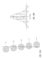
- Figs. 10A, 10B and 11A, 11B show a round laser beam traversing the rectangular narrow facet detection slit.
- Fig. 10B shows the resulting unfiltered electronic signal from the pulses under an envelope of what would be the signal if the laser were operating in a CW mode; the vertical scale in Fig. 10B is amplitude and the horizontal scale is scan position.
- Figs. 11A and 11B show graphically the response of the facet detector in terms of the broadened pulses from the above-described electronic filtering carried out by filter circuitry 171 of Fig. 9 and the sum of the signals (dotted line) from the individual pulses for two different arbitrarily chosen phases. Comparing Fig. 11A to Fig. 11B shows that the sum is independent of pulse phase.
- variable phase differences between the laser pulses and the data pixel clock signals are accommodated by appropriate choice of system parameters, of which a range have been found to be appropriate.
- One exemplary version for a 263 nm wavelength laser beam uses a pixel size of 160 nm, a spot size (1/e 2 ) of 320 nm, an AOM spot size (1/e 2 ) of 144 nm, a pixel period of 20 ns, and a laser period of 13 ns.
- the distance the beam scans between laser pulses is 104 nm
- the 1/e 2 radius of the image spot is 160 nm
- the distance the beam scans during the time the acoustic signal travels across the 1/e 2 diameter of the spot inside the AOM is 192 nm.
- the asynchronous embodiment it has been found to be satisfactory, in spite of the pulsing of the laser beam, to use several stages of a low pass filter network to broaden and make Gaussian the output signal from the facet detector PMT 168, to achieve facet detection of the pulsed laser beam.
- a low pass filter network for example, four series-connected low pass filter stages each having an RC time constant of 15 ns coupled to receive the output signal of PMT 168 provide sufficient signal smoothing for facet detection; this is filter circuitry 171 shown in Fig. 9.
- the filtering of the facet detector PMT 168 output signal thereby allows facet detection in the asynchronous embodiment.
Landscapes
- Physics & Mathematics (AREA)
- Optics & Photonics (AREA)
- Engineering & Computer Science (AREA)
- Plasma & Fusion (AREA)
- Mechanical Engineering (AREA)
- General Physics & Mathematics (AREA)
- Multimedia (AREA)
- Signal Processing (AREA)
- Mechanical Optical Scanning Systems (AREA)
- Lasers (AREA)
Claims (19)
- Générateur de motifs laser comprenant: un laser pulsé (100) générant un faisceau laser pulsé; un modulateur opto-acoustique (116) placé pour recevoir le faisceau pulsé et moduler le faisceau pulsé à l'aide d'un signal électrique définissant le motif; un dispositif de balayage (148, 152, 154) placé pour recevoir le faisceau pulsé modulé du modulateur et balayer le faisceau modulé d'un côté à l'autre d'un support (196); un déflecteur (140) dans un trajet du faisceau pulsé modulé entre le modulateur et le dispositif de balayage afin de dévier le faisceau; une lentille de balayage (160) placée entre le dispositif de balayage et le support pour focaliser le faisceau pulsé modulé et dévié sur le support; et un détecteur (168) pour détecter le faisceau pulsé modulé et dévié; comprenant de plus un circuit de commande (170) couplé au détecteur (168) et au déflecteur (140) afin de dévier le faisceau pulsé modulé en synchronisme avec les impulsions détectées du faisceau.
- Générateur de motifs laser selon la revendication 1, caractérisé en ce que le laser (100) est pulsé à une fréquence d'au moins 1 MHz.
- Générateur de motifs laser selon la revendication 1, caractérisé en ce que le dispositif de balayage (148, 152, 154) inclut un polygone tournant (148) ayant une pluralité de facettes réfléchissantes.
- Générateur de motifs laser selon la revendication 1, caractérisé en ce qu'un diamètre du faisceau pulsé modulé et dévié frappant le support est inférieur à 400 nm.
- Générateur de motifs laser selon la revendication 1, caractérisé en ce que le laser est un laser à semi-conducteur à fréquence quadruplée.
- Générateur de motifs laser selon la revendication 1, caractérisé en ce que le signal électrique représente un motif en échelle de gris à écrire sur le support.
- Générateur de motifs laser selon la revendication 1, caractérisé en ce qu'un temps de montée du modulateur est inférieur à une période de pulsation du faisceau.
- Générateur de motifs laser comprenant: un laser pulsé (100) générant un faisceau laser pulsé; un modulateur opto-acoustique (116) placé pour recevoir le faisceau pulsé et moduler le faisceau pulsé à l'aide d'un signal électrique définissant le motif; un dispositif de balayage (148, 152, 154) placé pour recevoir le faisceau pulsé modulé du modulateur et balayer le faisceau modulé d'un côté à l'autre d'un support (196); une lentille de balayage (160) entre le dispositif de balayage et le support afin de focaliser le faisceau pulsé modulé et dévié sur le support; dans lequel le générateur de motifs laser est conçu de telle manière qu'une cadence de pulsation du laser est égale ou supérieure à une cadence de pixel des pixels du motif et que la cadence de pulsation du laser (100) est asynchrone à la modulation du faisceau pulsé, ce qui fait qu'un motif défini sur le support par le faisceau pulsé modulé n'est pas aligné sur une grille fixe définie sur une surface du support.
- Générateur de motifs laser selon la revendication 8, caractérisé en ce qu'une phase d'une cadence de pulsation du laser pulsé est indépendante d'une fréquence de modulation du signal électrique.
- Générateur de motifs laser selon la revendication 1, caractérisé en ce que le faisceau laser est à une longueur d'onde inférieure ou égale à 355 nm quand il sort du laser.
- Générateur de motifs laser selon la revendication 8, caractérisé en ce que le faisceau laser pulsé est à une longueur d'onde inférieure ou égale à 355 nm quand il sort du laser pulsé.
- Procédé de présentation d'une pluralité de pixels sur un support à l'aide d'un faisceau laser, comprenant: la délivrance d'un faisceau laser pulsé depuis un laser pulsé (100); la modulation du faisceau laser pulsé à l'aide d'un signal électrique définissant les pixels; la déflexion du faisceau pulsé modulé en synchronisme avec les pulsations du faisceau; le balayage du faisceau modulé et dévié d'un côté à l'autre du support; la focalisation du faisceau balayé modulé et dévié sur le support; et la détection des pulsations du faisceau modulé et dévié pour commander la déflexion.
- Procédé selon la revendication 12, caractérisé en ce que le faisceau laser est pulsé à une fréquence d'au moins 1 MHz.
- Procédé selon la revendication 12, caractérisé en ce que le balayage inclut un polygone tournant ayant une pluralité de facettes réfléchissantes.
- Procédé selon la revendication 12, caractérisé en ce que le balayage inclut une déflexion opto-acoustique afin de synchroniser le balayage sur le faisceau pulsé.
- Procédé selon la revendication 12, caractérisé en ce qu'un diamètre du faisceau frappant le support est inférieur à 400 nm.
- Procédé selon la revendication 12, comprenant de plus la production du faisceau laser depuis un laser à semi-conducteur à fréquence quadruplée.
- Procédé selon la revendication 12, caractérisé en ce que le signal électrique représente un motif en échelle de gris à écrire sur le support.
- Procédé selon la revendication 12, caractérisé en ce qu'un temps de montée d'un modulateur au cours de l'étape de modulation est inférieur à une période de pulsation du faisceau pulsé.
Applications Claiming Priority (3)
| Application Number | Priority Date | Filing Date | Title |
|---|---|---|---|
| US769169 | 1996-12-18 | ||
| US08/769,169 US6037967A (en) | 1996-12-18 | 1996-12-18 | Short wavelength pulsed laser scanner |
| PCT/US1997/022053 WO1998027450A1 (fr) | 1996-12-18 | 1997-12-10 | Scanner laser pulse a courte longueur d'onde courte |
Publications (2)
| Publication Number | Publication Date |
|---|---|
| EP0904559A1 EP0904559A1 (fr) | 1999-03-31 |
| EP0904559B1 true EP0904559B1 (fr) | 2001-10-24 |
Family
ID=25084671
Family Applications (1)
| Application Number | Title | Priority Date | Filing Date |
|---|---|---|---|
| EP97953077A Expired - Lifetime EP0904559B1 (fr) | 1996-12-18 | 1997-12-10 | Dispositif de balayage a laser pulse a longueur d'onde courte |
Country Status (7)
| Country | Link |
|---|---|
| US (1) | US6037967A (fr) |
| EP (1) | EP0904559B1 (fr) |
| JP (1) | JP2000507003A (fr) |
| KR (1) | KR19990082646A (fr) |
| CA (1) | CA2244712A1 (fr) |
| DE (1) | DE69707671T2 (fr) |
| WO (1) | WO1998027450A1 (fr) |
Families Citing this family (70)
| Publication number | Priority date | Publication date | Assignee | Title |
|---|---|---|---|---|
| GB9802688D0 (en) * | 1998-02-06 | 1998-07-29 | Marconi Gec Ltd | Improvements in or relating to sound detection |
| DE19829986C1 (de) * | 1998-07-04 | 2000-03-30 | Lis Laser Imaging Systems Gmbh | Verfahren zur Direktbelichtung von Leiterplattensubstraten |
| DE69819044T2 (de) | 1998-08-20 | 2004-08-12 | Orbotech Ltd. | Laserwiederholfrequenzvervielfacher |
| IL133889A (en) | 2000-01-05 | 2007-03-08 | Orbotech Ltd | Pulse light pattern writer |
| US6555781B2 (en) * | 1999-05-10 | 2003-04-29 | Nanyang Technological University | Ultrashort pulsed laser micromachining/submicromachining using an acoustooptic scanning device with dispersion compensation |
| US6246706B1 (en) | 1999-05-27 | 2001-06-12 | Spectra Physics Lasers, Inc. | Laser writing method and apparatus |
| SE516914C2 (sv) * | 1999-09-09 | 2002-03-19 | Micronic Laser Systems Ab | Metoder och rastrerare för högpresterande mönstergenerering |
| JP2001255661A (ja) * | 2000-01-05 | 2001-09-21 | Orbotech Ltd | パルス光パターン書込み装置 |
| US6552779B2 (en) * | 2000-05-25 | 2003-04-22 | Ball Semiconductor, Inc. | Flying image of a maskless exposure system |
| US6560248B1 (en) * | 2000-06-08 | 2003-05-06 | Mania Barco Nv | System, method and article of manufacture for improved laser direct imaging a printed circuit board utilizing a mode locked laser and scophony operation |
| US6625181B1 (en) * | 2000-10-23 | 2003-09-23 | U.C. Laser Ltd. | Method and apparatus for multi-beam laser machining |
| US7062354B2 (en) | 2000-11-08 | 2006-06-13 | Orbotech Ltd. | Multi-layer printed circuit board fabrication system and method |
| JP4514317B2 (ja) * | 2000-11-27 | 2010-07-28 | 株式会社ミツトヨ | 露光装置 |
| US7453486B2 (en) * | 2000-12-13 | 2008-11-18 | Orbotech Ltd | Pulse light pattern writer |
| AU2002245119A1 (en) | 2000-12-15 | 2002-07-30 | Sloan-Kettering Institute For Cancer Research | Beam-steering of multi-chromatic light using acousto-optical deflectors and dispersion-compensatory optics |
| WO2002054837A2 (fr) * | 2001-01-04 | 2002-07-11 | Laser Imaging Systems Gmbh & Co. Kg | Dispositif de formation directe de motifs |
| US6689985B2 (en) | 2001-01-17 | 2004-02-10 | Orbotech, Ltd. | Laser drill for use in electrical circuit fabrication |
| US6472239B2 (en) * | 2001-04-02 | 2002-10-29 | Micron Technology, Inc. | Method for fabricating semiconductor components |
| US6680213B2 (en) | 2001-04-02 | 2004-01-20 | Micron Technology, Inc. | Method and system for fabricating contacts on semiconductor components |
| US6532097B1 (en) * | 2001-10-11 | 2003-03-11 | Applied Materials, Inc. | Image registration apparatus having an adjustable reflective diffraction grating and method |
| WO2003033199A1 (fr) * | 2001-10-19 | 2003-04-24 | U.C. Laser Ltd. | Procede d'amelioration de l'alignement de tranches |
| US6658315B2 (en) * | 2001-10-31 | 2003-12-02 | Ball Semiconductor, Inc. | Non-synchronous control of pulsed light |
| NL1020709C2 (nl) * | 2002-05-29 | 2003-12-02 | Ind Automation Integrators I A | Van een AOD voorziene laserbewerkinrichting. |
| US20040195222A1 (en) * | 2002-12-25 | 2004-10-07 | Semiconductor Energy Laboratory Co., Ltd. | Laser irradiation method, laser irradiation apparatus, and method for manufacturing semiconductor device |
| US7483196B2 (en) | 2003-09-23 | 2009-01-27 | Applied Materials, Inc. | Apparatus for multiple beam deflection and intensity stabilization |
| EP1537938A3 (fr) * | 2003-12-02 | 2009-02-18 | Semiconductor Energy Laboratory Co., Ltd. | Appareil d'irradiation laser, méthode d'irradiation laser, et méthode de fabrication de dispositif semi-conducteur |
| EP1553643A3 (fr) * | 2003-12-26 | 2009-01-21 | Sel Semiconductor Energy Laboratory Co., Ltd. | Méthode d'irradiation par laser et méthode de fabrication d'un film cristallin et semiconducteur |
| US20050283498A1 (en) * | 2004-06-22 | 2005-12-22 | Taiwan Semiconductor Manufacturing Company, Ltd. | System and method to build, retrieve and track information in a knowledge database for trouble shooting purposes |
| US7403265B2 (en) * | 2005-03-30 | 2008-07-22 | Asml Netherlands B.V. | Lithographic apparatus and device manufacturing method utilizing data filtering |
| CN101203808A (zh) * | 2005-04-15 | 2008-06-18 | 麦克罗尼克激光系统公司 | 图像增强技术 |
| CA2621001C (fr) * | 2005-08-31 | 2012-10-16 | Heidelberg Instruments Mikrotechnik Gmbh | Dispositif pour diviser et moduler optiquement un rayonnement electromagnetique |
| DE102006040843B4 (de) * | 2005-08-31 | 2015-04-16 | Heidelberger Instruments Mikrotechnik Gmbh | Vorrichtung zur optischen Aufspaltung und Modulation von elektromagnetischer Strahlung |
| US9889043B2 (en) * | 2006-01-20 | 2018-02-13 | Lensar, Inc. | System and apparatus for delivering a laser beam to the lens of an eye |
| GB2438600B (en) * | 2006-05-19 | 2008-07-09 | Exitech Ltd | Method for patterning thin films on moving substrates |
| CN1870234B (zh) * | 2006-06-15 | 2011-07-20 | 友达光电股份有限公司 | 薄膜晶体管的制作方法 |
| DE102006034755A1 (de) * | 2006-07-24 | 2008-01-31 | Carl Zeiss Smt Ag | Optische Vorrichtung sowie Verfahren zur Korrektur bzw. Verbesserung des Abbildungsverhaltens einer optischen Vorrichtung |
| US7706420B2 (en) * | 2006-09-05 | 2010-04-27 | Corning Incorporated | Optical power modulation at high frequency |
| US20080090396A1 (en) * | 2006-10-06 | 2008-04-17 | Semiconductor Energy Laboratory Co., Ltd. | Light exposure apparatus and method for making semiconductor device formed using the same |
| JP5007192B2 (ja) * | 2006-10-06 | 2012-08-22 | 株式会社半導体エネルギー研究所 | 半導体装置の作製方法 |
| WO2008091898A1 (fr) * | 2007-01-23 | 2008-07-31 | Imra America, Inc. | Impression de microtexture par laser ultra-bref |
| DE102007012815B4 (de) * | 2007-03-16 | 2024-06-06 | Dmg Mori Ultrasonic Lasertec Gmbh | Verfahren und Vorrichtung zur Bildung eines Gesenks |
| ITPD20070201A1 (it) * | 2007-06-08 | 2008-12-09 | Helios Technology Societa A Re | Macchina per la rimozione di superfici di semiconduttori, ed in particolare di superfici con circuiti integrati |
| GB2457720A (en) * | 2008-02-23 | 2009-08-26 | Philip Thomas Rumsby | Method for laser processing on the opposite sides of thin transparent substrates |
| IL198719A0 (en) * | 2009-05-12 | 2010-02-17 | Orbotech Ltd | Optical imaging system |
| CN102598310A (zh) * | 2009-09-18 | 2012-07-18 | 应用材料公司 | 背接触太阳能电池中的通孔的激光钻孔 |
| JP5604745B2 (ja) * | 2010-11-11 | 2014-10-15 | 株式会社ブイ・テクノロジー | 露光装置 |
| JP5667545B2 (ja) * | 2011-10-24 | 2015-02-12 | 東京エレクトロン株式会社 | 液処理装置および液処理方法 |
| JP5856824B2 (ja) * | 2011-11-28 | 2016-02-10 | オリンパス株式会社 | 光走査装置および走査型顕微鏡装置 |
| JP6125649B2 (ja) * | 2012-10-31 | 2017-05-10 | ハンズ レーザー テクノロジー インダストリー グループ カンパニー リミテッド | 紫外レーザマーキングFθレンズ及びレーザ加工デバイス |
| JP6318572B2 (ja) * | 2013-11-19 | 2018-05-09 | 株式会社リコー | 画像処理装置及び方法、並びに画像形成装置 |
| TWI709006B (zh) * | 2014-04-01 | 2020-11-01 | 日商尼康股份有限公司 | 圖案描繪裝置及圖案描繪方法 |
| JP6349924B2 (ja) * | 2014-04-28 | 2018-07-04 | 株式会社ニコン | パターン描画装置 |
| CN110095862B (zh) * | 2014-04-28 | 2021-08-27 | 株式会社尼康 | 图案曝光装置 |
| JP2015210517A (ja) * | 2014-09-09 | 2015-11-24 | 株式会社ニコン | パターン描画装置、パターン描画方法、および、デバイス製造方法 |
| JP2016068149A (ja) * | 2014-10-02 | 2016-05-09 | 株式会社ディスコ | レーザー加工装置 |
| US10286488B2 (en) | 2015-03-06 | 2019-05-14 | Intel Corporation | Acousto-optics deflector and mirror for laser beam steering |
| KR20250037607A (ko) | 2015-09-09 | 2025-03-17 | 일렉트로 싸이언티픽 인더스트리이즈 인코포레이티드 | 작업물들을 레이저 가공하기 위한 레이저 가공 장치, 방법들 및 관련된 배열들 |
| CN109791280B (zh) * | 2016-10-04 | 2022-01-07 | 株式会社尼康 | 光束扫描装置 |
| JP6997566B2 (ja) * | 2017-09-14 | 2022-01-17 | 株式会社ディスコ | レーザー加工装置 |
| KR102148929B1 (ko) * | 2017-11-24 | 2020-08-28 | 주식회사 이오테크닉스 | 4f 앵글제어 광학계를 포함하는 레이저 가공 장치 |
| JP2018045254A (ja) * | 2017-12-11 | 2018-03-22 | 株式会社ニコン | パターン描画装置 |
| KR102081199B1 (ko) * | 2018-02-13 | 2020-02-25 | 주식회사 이오테크닉스 | 4f 앵글제어 광학계를 포함하는 레이저 가공 시스템 |
| JP6504293B2 (ja) * | 2018-03-23 | 2019-04-24 | 株式会社ニコン | パターン描画装置 |
| JP6587026B2 (ja) * | 2018-10-30 | 2019-10-09 | 株式会社ニコン | パターン露光装置 |
| DE102018132001A1 (de) * | 2018-12-12 | 2020-06-18 | Laser Imaging Systems Gmbh | Vorrichtung zum Belichten von plattenförmigen Werkstücken mit hohem Durchsatz |
| US11237386B2 (en) | 2020-03-11 | 2022-02-01 | Rohr, Inc. | Substrate perforation system and method using polygon mirror(s) |
| KR102793341B1 (ko) * | 2020-05-21 | 2025-04-09 | 삼성디스플레이 주식회사 | 레이저 장치 |
| CN112859538B (zh) * | 2021-01-08 | 2021-10-08 | 华中科技大学 | 一种基于声光偏转器的双光子聚合激光直写加工系统 |
| EP4079446B1 (fr) * | 2021-04-19 | 2024-09-11 | Akzenta Paneele + Profile GmbH | Procédé de fabrication d'un panneau décoratif à structuration améliorée |
| CN117600647A (zh) * | 2023-11-01 | 2024-02-27 | 华中科技大学 | 一种声光动态调焦模块及三维扫描系统 |
Family Cites Families (25)
| Publication number | Priority date | Publication date | Assignee | Title |
|---|---|---|---|---|
| US4044363A (en) * | 1974-12-23 | 1977-08-23 | Dymo Industries, Inc. | Laser photocomposition system and method |
| US4180822A (en) * | 1978-04-13 | 1979-12-25 | Rca Corporation | Optical scanner and recorder |
| US4213158A (en) * | 1978-06-28 | 1980-07-15 | Xerox Corporation | Optical data recording system utilizing acoustic pulse imaging to minimize image blur |
| US4205348A (en) * | 1978-07-05 | 1980-05-27 | Xerox Corporation | Laser scanning utilizing facet tracking and acousto pulse imaging techniques |
| US4307409A (en) * | 1980-05-27 | 1981-12-22 | Sperry Corporation | Multi-aperture, feedback system for a laser scanner |
| US4321564A (en) * | 1980-06-18 | 1982-03-23 | Litton Systems, Inc. | Sequential beam switching of acousto-optic modulator |
| US4883352A (en) * | 1984-06-21 | 1989-11-28 | American Telephone And Telegraph Company | Deep-uv lithography |
| FR2568688B1 (fr) * | 1984-08-03 | 1986-09-05 | Thomson Csf | Systeme emetteur-recepteur pour imagerie laser |
| JPS63110722A (ja) * | 1986-10-29 | 1988-05-16 | Hitachi Ltd | 露光照明装置 |
| JPS63193130A (ja) * | 1987-02-05 | 1988-08-10 | Canon Inc | 光量制御装置 |
| US5156943A (en) * | 1987-10-25 | 1992-10-20 | Whitney Theodore R | High resolution imagery systems and methods |
| US4912487A (en) * | 1988-03-25 | 1990-03-27 | Texas Instruments Incorporated | Laser scanner using focusing acousto-optic device |
| JP3003864B2 (ja) * | 1988-04-14 | 2000-01-31 | 株式会社リコー | 固体走査型記録ヘッドの駆動方法及びその装置 |
| US4947186A (en) * | 1988-09-22 | 1990-08-07 | The Aerospace Corporation | Apparatus and method for a UV laser image recorder |
| JP2937361B2 (ja) * | 1989-09-29 | 1999-08-23 | 日本電気株式会社 | レーザ加工機 |
| US5327338A (en) * | 1990-01-31 | 1994-07-05 | Etec Systems, Inc. | Scanning laser lithography system alignment apparatus |
| US5227839A (en) * | 1991-06-24 | 1993-07-13 | Etec Systems, Inc. | Small field scanner |
| US5377212A (en) * | 1991-10-17 | 1994-12-27 | Hitachi, Ltd. | Solid-state laser device including uniaxial laser crystal emitting linearly polarized fundamental wave and nonlinear optical crystal emitting linearly polarized harmonic wave |
| US5264872A (en) * | 1992-09-18 | 1993-11-23 | Xerox Corporation | Raster output scanner with improved process direction registration |
| US5386221A (en) * | 1992-11-02 | 1995-01-31 | Etec Systems, Inc. | Laser pattern generation apparatus |
| JPH06235944A (ja) * | 1993-02-08 | 1994-08-23 | Dainippon Screen Mfg Co Ltd | 光ビーム走査方法 |
| JPH06302491A (ja) * | 1993-04-15 | 1994-10-28 | Nikon Corp | 露光量制御装置 |
| US5311321A (en) * | 1993-04-22 | 1994-05-10 | Corporation For Laser Optics Research | Laser video imaging system with pulse backtrack and method |
| EP0627643B1 (fr) * | 1993-06-03 | 1999-05-06 | Hamamatsu Photonics K.K. | Système optique de balayage à laser utilisant un axicon |
| US5673134A (en) * | 1994-07-15 | 1997-09-30 | Sony Corporation | Light exposure and illuminating apparatus |
-
1996
- 1996-12-18 US US08/769,169 patent/US6037967A/en not_active Expired - Lifetime
-
1997
- 1997-12-10 CA CA002244712A patent/CA2244712A1/fr not_active Abandoned
- 1997-12-10 KR KR1019980706388A patent/KR19990082646A/ko not_active Ceased
- 1997-12-10 EP EP97953077A patent/EP0904559B1/fr not_active Expired - Lifetime
- 1997-12-10 WO PCT/US1997/022053 patent/WO1998027450A1/fr not_active Ceased
- 1997-12-10 DE DE69707671T patent/DE69707671T2/de not_active Expired - Fee Related
- 1997-12-10 JP JP10527749A patent/JP2000507003A/ja not_active Ceased
Also Published As
| Publication number | Publication date |
|---|---|
| KR19990082646A (ko) | 1999-11-25 |
| EP0904559A1 (fr) | 1999-03-31 |
| US6037967A (en) | 2000-03-14 |
| WO1998027450A1 (fr) | 1998-06-25 |
| CA2244712A1 (fr) | 1998-06-25 |
| JP2000507003A (ja) | 2000-06-06 |
| DE69707671T2 (de) | 2002-08-01 |
| DE69707671D1 (de) | 2001-11-29 |
Similar Documents
| Publication | Publication Date | Title |
|---|---|---|
| EP0904559B1 (fr) | Dispositif de balayage a laser pulse a longueur d'onde courte | |
| CN101137927B (zh) | 用于多光束偏转和强度稳定的装置 | |
| US7259777B2 (en) | Scanner system | |
| US4650983A (en) | Focusing apparatus for projection optical system | |
| US9551942B2 (en) | Controller for optical device, exposure method and apparatus, and method for manufacturing device | |
| US4796038A (en) | Laser pattern generation apparatus | |
| JP4495898B2 (ja) | 改良型パターン・ジェネレータ | |
| CN111512233A (zh) | 图案描绘装置 | |
| US20040112879A1 (en) | Identification-code laser marking method and apparatus | |
| KR100467307B1 (ko) | 레이저 묘화방법과 그 장치 | |
| US6975443B2 (en) | Multi-beam pattern generator | |
| EP1272903B1 (fr) | Appareil destine a produire un motif laser sur un masque photographique et procedes associes | |
| JP2003318096A (ja) | 光ビーム照射装置 | |
| JPH08213299A (ja) | パターン露光装置 | |
| TWI807775B (zh) | 描繪裝置以及描繪方法 | |
| JP3191438B2 (ja) | 光学記録方法及び光学記録装置 | |
| KR100500771B1 (ko) | 스캐닝-슬릿노광장치 | |
| JPH10172901A (ja) | 走査型投影露光装置及びそれを用いたデバイスの製造方法 | |
| WO2024149725A1 (fr) | Dispositif d'écriture laser et procédé de fonctionnement de dispositif d'écriture laser | |
| HK1145048A (en) | Control device, exposure method, and exposure device |
Legal Events
| Date | Code | Title | Description |
|---|---|---|---|
| PUAI | Public reference made under article 153(3) epc to a published international application that has entered the european phase |
Free format text: ORIGINAL CODE: 0009012 |
|
| 17P | Request for examination filed |
Effective date: 19980825 |
|
| AK | Designated contracting states |
Kind code of ref document: A1 Designated state(s): DE FR GB IT NL SE |
|
| 17Q | First examination report despatched |
Effective date: 19991129 |
|
| GRAG | Despatch of communication of intention to grant |
Free format text: ORIGINAL CODE: EPIDOS AGRA |
|
| GRAG | Despatch of communication of intention to grant |
Free format text: ORIGINAL CODE: EPIDOS AGRA |
|
| GRAH | Despatch of communication of intention to grant a patent |
Free format text: ORIGINAL CODE: EPIDOS IGRA |
|
| GRAH | Despatch of communication of intention to grant a patent |
Free format text: ORIGINAL CODE: EPIDOS IGRA |
|
| GRAA | (expected) grant |
Free format text: ORIGINAL CODE: 0009210 |
|
| AK | Designated contracting states |
Kind code of ref document: B1 Designated state(s): DE FR GB IT NL SE |
|
| PG25 | Lapsed in a contracting state [announced via postgrant information from national office to epo] |
Ref country code: IT Free format text: LAPSE BECAUSE OF FAILURE TO SUBMIT A TRANSLATION OF THE DESCRIPTION OR TO PAY THE FEE WITHIN THE PRE;WARNING: LAPSES OF ITALIAN PATENTS WITH EFFECTIVE DATE BEFORE 2007 MAY HAVE OCCURRED AT ANY TIME BEFORE 2007. THE CORRECT EFFECTIVE DATE MAY BE DIFFERENT FROM THE ONE RECORDED.SCRIBED TIME-LIMIT Effective date: 20011024 Ref country code: FR Free format text: LAPSE BECAUSE OF FAILURE TO SUBMIT A TRANSLATION OF THE DESCRIPTION OR TO PAY THE FEE WITHIN THE PRESCRIBED TIME-LIMIT Effective date: 20011024 |
|
| REF | Corresponds to: |
Ref document number: 69707671 Country of ref document: DE Date of ref document: 20011129 |
|
| REG | Reference to a national code |
Ref country code: GB Ref legal event code: IF02 |
|
| PG25 | Lapsed in a contracting state [announced via postgrant information from national office to epo] |
Ref country code: SE Free format text: LAPSE BECAUSE OF FAILURE TO SUBMIT A TRANSLATION OF THE DESCRIPTION OR TO PAY THE FEE WITHIN THE PRESCRIBED TIME-LIMIT Effective date: 20020124 |
|
| RAP2 | Party data changed (patent owner data changed or rights of a patent transferred) |
Owner name: APPLIED MATERIALS, INC. |
|
| EN | Fr: translation not filed | ||
| PLBE | No opposition filed within time limit |
Free format text: ORIGINAL CODE: 0009261 |
|
| STAA | Information on the status of an ep patent application or granted ep patent |
Free format text: STATUS: NO OPPOSITION FILED WITHIN TIME LIMIT |
|
| NLT2 | Nl: modifications (of names), taken from the european patent patent bulletin |
Owner name: APPLIED MATERIALS, INC. |
|
| 26N | No opposition filed | ||
| NLS | Nl: assignments of ep-patents |
Owner name: APPLIED MATERIALS, INC. |
|
| REG | Reference to a national code |
Ref country code: GB Ref legal event code: 732E |
|
| PGFP | Annual fee paid to national office [announced via postgrant information from national office to epo] |
Ref country code: GB Payment date: 20061106 Year of fee payment: 10 |
|
| PGFP | Annual fee paid to national office [announced via postgrant information from national office to epo] |
Ref country code: NL Payment date: 20061108 Year of fee payment: 10 |
|
| PGFP | Annual fee paid to national office [announced via postgrant information from national office to epo] |
Ref country code: DE Payment date: 20061229 Year of fee payment: 10 |
|
| GBPC | Gb: european patent ceased through non-payment of renewal fee |
Effective date: 20071210 |
|
| NLV4 | Nl: lapsed or anulled due to non-payment of the annual fee |
Effective date: 20080701 |
|
| PG25 | Lapsed in a contracting state [announced via postgrant information from national office to epo] |
Ref country code: DE Free format text: LAPSE BECAUSE OF NON-PAYMENT OF DUE FEES Effective date: 20080701 |
|
| PG25 | Lapsed in a contracting state [announced via postgrant information from national office to epo] |
Ref country code: NL Free format text: LAPSE BECAUSE OF NON-PAYMENT OF DUE FEES Effective date: 20080701 |
|
| PG25 | Lapsed in a contracting state [announced via postgrant information from national office to epo] |
Ref country code: GB Free format text: LAPSE BECAUSE OF NON-PAYMENT OF DUE FEES Effective date: 20071210 |