EP0903777A1 - Musterformverfahren - Google Patents
Musterformverfahren Download PDFInfo
- Publication number
- EP0903777A1 EP0903777A1 EP97946114A EP97946114A EP0903777A1 EP 0903777 A1 EP0903777 A1 EP 0903777A1 EP 97946114 A EP97946114 A EP 97946114A EP 97946114 A EP97946114 A EP 97946114A EP 0903777 A1 EP0903777 A1 EP 0903777A1
- Authority
- EP
- European Patent Office
- Prior art keywords
- reflective coating
- bottom anti
- gas
- organic bottom
- etching
- Prior art date
- Legal status (The legal status is an assumption and is not a legal conclusion. Google has not performed a legal analysis and makes no representation as to the accuracy of the status listed.)
- Withdrawn
Links
Images


Classifications
-
- G—PHYSICS
- G03—PHOTOGRAPHY; CINEMATOGRAPHY; ANALOGOUS TECHNIQUES USING WAVES OTHER THAN OPTICAL WAVES; ELECTROGRAPHY; HOLOGRAPHY
- G03F—PHOTOMECHANICAL PRODUCTION OF TEXTURED OR PATTERNED SURFACES, e.g. FOR PRINTING, FOR PROCESSING OF SEMICONDUCTOR DEVICES; MATERIALS THEREFOR; ORIGINALS THEREFOR; APPARATUS SPECIALLY ADAPTED THEREFOR
- G03F7/00—Photomechanical, e.g. photolithographic, production of textured or patterned surfaces, e.g. printing surfaces; Materials therefor, e.g. comprising photoresists; Apparatus specially adapted therefor
- G03F7/004—Photosensitive materials
- G03F7/09—Photosensitive materials characterised by structural details, e.g. supports, auxiliary layers
- G03F7/091—Photosensitive materials characterised by structural details, e.g. supports, auxiliary layers characterised by antireflection means or light filtering or absorbing means, e.g. anti-halation, contrast enhancement
-
- H—ELECTRICITY
- H10—SEMICONDUCTOR DEVICES; ELECTRIC SOLID-STATE DEVICES NOT OTHERWISE PROVIDED FOR
- H10P—GENERIC PROCESSES OR APPARATUS FOR THE MANUFACTURE OR TREATMENT OF DEVICES COVERED BY CLASS H10
- H10P50/00—Etching of wafers, substrates or parts of devices
- H10P50/20—Dry etching; Plasma etching; Reactive-ion etching
- H10P50/28—Dry etching; Plasma etching; Reactive-ion etching of insulating materials
- H10P50/286—Dry etching; Plasma etching; Reactive-ion etching of insulating materials of organic materials
- H10P50/287—Dry etching; Plasma etching; Reactive-ion etching of insulating materials of organic materials by chemical means
-
- H—ELECTRICITY
- H10—SEMICONDUCTOR DEVICES; ELECTRIC SOLID-STATE DEVICES NOT OTHERWISE PROVIDED FOR
- H10P—GENERIC PROCESSES OR APPARATUS FOR THE MANUFACTURE OR TREATMENT OF DEVICES COVERED BY CLASS H10
- H10P50/00—Etching of wafers, substrates or parts of devices
- H10P50/71—Etching of wafers, substrates or parts of devices using masks for conductive or resistive materials
Definitions
- the present invention relates to a pattern formation method for forming a resist pattern composed of a resist film. More particularly, it relates to the technique of performing dry etching with respect to an organic bottom anti-reflective coating deposited under the resist film by using the resist pattern as a mask.
- the reflectivity of light reflected from a substrate after exposing a resist film becomes higher so that the reflected light from the substrate is more likely to cause variations in the size of a resist pattern.
- the variations in the size of the resist pattern are produced as follows. After exposing the resist film, the light is reflected from the substrate underlying the resist film and incident again on the resist film to re-expose the resist film including a portion which should not be exposed.
- ARC organic anti-reflection coating
- an organic bottom anti-reflective coating 12 is deposited on an underlying film 11 (such as a polysilicon film, a silicon oxide film, or a tungsten silicide film) to have a flat surface.
- an underlying film 11 such as a polysilicon film, a silicon oxide film, or a tungsten silicide film
- a resist film 13 composed of a positive resist is deposited on the organic bottom anti-reflective coating 12 .
- the pattern formation method using the organic bottom anti-reflective coating 12 as described above presents problems during dry etching performed with respect to the organic bottom anti-reflective coating 12 , which are easily produced variations in the size of the organic bottom anti-reflective coating 12 , low selectivity of the organic bottom anti-reflective coating 12 to the underlying film 11 , and an increased number of particles generated in a reaction chamber in which etching is performed.
- the cause thereof may be simultaneous etching of the resist pattern 15 with the etching of the organic bottom anti-reflective coating 12 since the resist pattern 15 is made of a carbon-based material, similarly to the organic bottom anti-reflective coating 12 .
- the cause thereof may be particles generated from the organic bottom anti-reflective coating 12 during the etching of the organic bottom anti-reflective coating 12 .
- the present inventors performed dry etching with respect to the organic bottom anti-reflective coating 12 by using Cl 2 /O 2 -based gas and encountered another problem, which will be described below.
- a dry-etching apparatus can be selected from various etching apparatus, the description will be given to the case where dry etching was performed by using a first etching apparatus shown in Figure 2 .
- the first etching apparatus comprises a grounded chamber 21 having an inner wall covered with an insulator such as ceramic, alumina, or quartz.
- An inner circumferential wall of the chamber 21 is provided with a first lateral electrode 22A , a second lateral electrode 22B , and a third lateral electrode 22C , which are equally spaced therearound.
- the first, second, and third lateral electrodes 22A , 22B , and 22C receive respective supplies of high-frequency power of 54.24 MHz from a first high-frequency power source 23A , a second high-frequency power source 23B , and a third high-frequency power source 23C via a matching circuit not shown.
- the supplies of high-frequency power are equal in discharge power but progressively shifted in phase by approximately 120°.
- phase of high-frequency power supplied to the second lateral electrode 22B is 120° leading the phase of high-frequency power supplied to the first lateral electrode 22A and the phase of high-frequency power supplied to the third lateral electrode 22C is 120° lagging behind the phase of high-frequency power supplied to the first lateral electrode 22A .
- a phase shifter not shown produces a 120° phase shift between the supplies of high-frequency power from each adjacent two of the first to third high-frequency power sources 23A to 23C .
- An earth electrode 24 is disposed on the inner bottom portion of the chamber 21 .
- a sample stage 25 serving as a lower electrode for holding a substrate is provided on the earth electrode 24 .
- a bias high-frequency voltage is applied from a fourth high-frequency power source 26 to the sample stage 25 .
- the chamber 21 is provided with a gas inlet for introducing etching gas into the chamber 21 via a mass flow controller and with a turbo pump for adjusting pressure in the chamber 21 to be about 0.1 to 10 Pa, though they are not shown in the drawings.
- a silicon oxide film 42 is thermally grown on a silicon wafer 41 , followed by a polysilicon film 43 deposited as an underlying film on the thermally grown silicon oxide film 42 . Thereafter, an organic bottom anti-reflective coating 44 with a film thickness of 150 nm and a resist film are deposited sequentially on the polysilicon film 43 . Then, etching is performed with respect to the resist film to form a resist pattern 45 composed of the resist film.
- LEP Lisajous Electron Plasma
- RF Radio Frequency
- the polysilicon film 43 underlying the organic bottom anti-reflective coating 44 is also etched, so that surface roughness is observed at the polysilicon film 43 .
- etching performed with respect to the organic bottom anti-reflective coating 44 has thus caused surface roughness at the polysilicon film 43 , roughness remains on the polysilicon film 43 formed into a pattern, which presents a serious problem to practical applications.
- the present inventors also performed dry etching with respect to the organic bottom anti-reflective coating by using N 2 /O 2 -based gas and encountered still another problem, which will be described below.
- a description will be given to a method of etching performed with respect to the organic bottom anti-reflective coating by using N 2 /O 2 -based gas.
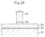
- a dry-etching apparatus can be selected from various etching apparatus, the description will be given to the case where dry etching was performed by using a second etching apparatus shown in Figure 3 .
- the second etching apparatus comprises a grounded chamber 31 having an inner wall covered with an insulator such as ceramic, alumina, or quartz.
- an inductively coupled coil 32 is disposed in the upper part thereof, while a sample stage 33 is disposed on an earth electrode 34 in the lower part thereof.
- One end of the inductively coupled coil 32 receives high-frequency power of 13.56 MHz applied thereto from a first high-frequency power supply 35 via a matching circuit not shown.
- the sample stage 33 receives high-frequency power of 13.56 MHz applied thereto from a second high-frequency power supply 36 .
- the other end of the inductively coupled coil 32 is connected to the sidewall of the chamber 31 and thereby grounded.
- the chamber 31 is provided with a gas inlet for introducing etching gas into the chamber 31 via a mass flow controller and with a turbo pump for adjusting pressure in the chamber 31 to about 0.1 to 10 Pa, though they are not shown in the drawings.
- a silicon oxide film 42 is thermally grown on a silicon wafer 41 , followed by a polysilicon film 43 deposited as an underlying film on the thermally grown silicon oxide film 42 . Thereafter, an organic bottom anti-reflective coating 44 with a film thickness of 150 nm and a resist film are deposited sequentially on the polysilicon film 43 . Then, etching is performed with respect to the resist film to form a resist pattern 45 composed of the resist film.
- the silicon wafer 41 as a target substrate was visually inspected in the dark field under a microscope and a large number of (about 100 residues per 3 mm 2 ) were observed.
- Such foreign residues resulting from etching performed with respect to the organic bottom anti-reflective coating 44 present a serious problem to practical applications, since the foreign residues are transferred to the polysilicon film 43 while it is etched in the subsequent step.
- a first object of the present invention is to pattern an organic bottom anti-reflective coating by dry etching such that the patterned organic bottom anti-reflective coating exhibits vertical profiles, an excellent size-varying property, and high selectivity to the underlying film, while no surface roughness is observed at the underlying film.
- a second object of the present invention is to pattern an organic bottom anti-reflective coating by dry etching such that the patterned organic bottom anti-reflective coating exhibits vertical profiles, an excellent size-varying property, and high selectivity to the underlying film, while no foreign residue is produced.
- Figure 21 is a plan view of the resist pattern overlying the region with surface roughness of the polysilicon film as the underlying film.
- the three sides of the resist pattern having an L-shaped configuration define a narrow region where the spacing between the opposed sides is 0.3 ⁇ m.
- the polysilicon film as the underlying film is covered with the organic bottom anti-reflective coating before dry etching is performed with respect to the organic bottom anti-reflective coating by using Cl 2 /O 2 -based etching gas.
- Figure 21 shows a plan view at the stage at which the etching of the organic bottom anti-reflective coating is completed.
- Cl 2 -based gas If consideration is given to Cl 2 -based gas, it etches not only the organic bottom anti-reflective coating but also the polysilicon film since Cl 2 -based gas is halogen-based gas. In the narrow region surrounded by the resist pattern, therefore, not only the organic bottom anti-reflective coating but also the polysilicon film as the underlying film is etched, resulting in surface roughness observed at the polysilicon film in the narrow region surrounded by the resist pattern.
- the foregoing problem also occurs when the underlying film is composed of a silicon-based film since the Cl 2 /O 2 -based etching gas also etches a silicon-based underling film such as an amorphous silicon film, a polysilicon film, or a tungsten silicide film besides the polysilicon film.
- the present inventors have found that the foreign residues contain silicon as the main component.
- the material of the organic bottom anti-reflective coating (CD9TM commercially available from Brewer Science Co., U.S.A.) in use was analyzed for an inorganic component by emission spectral analysis and a silicon component on the order of 10 ppm was detected from the material of the organic bottom anti-reflective coating.
- N 2 /O 2 -based gas it is capable of etching the organic component of the organic bottom anti-reflective coating but incapable of etching the silicon-based component. If an impurity of silicon is contained in the organic bottom anti-reflective coating, silicon contained therein remains without being etched away and the remaining silicon may serve as a source of the foreign residues.
- a first pattern formation method has been achieved based on the foregoing first knowledge and comprises: a first step of depositing an organic bottom anti-reflective coating on an underlying film formed on a substrate; a second step of forming a resist pattern on the organic bottom anti-reflective coating; and a third step of performing dry etching with respect to the organic bottom anti-reflective coating masked with the resist pattern to form an anti-reflective coating pattern composed of the organic bottom anti-reflective coating, wherein the third step includes the step of performing dry etching by using etching gas containing gas having a S component to form the anti-reflective coating pattern.
- the S component contained in etching gas has a low probability of reacting with Si so that etching gas will not etch the underlying film containing Si such as the polysilicon film formed under the organic bottom anti-reflective coating nor cause local surface roughness at the underlying film.
- the organic bottom anti-reflective coating has an excellent size-varying property after etching.
- the etching gas used in the third step is preferably SO 2 /O 2 -based gas.
- the adjustment of the ratio of O 2 to SO 2 in etching gas facilitates control of the size-varying property of the organic bottom anti-reflective coating after etching.
- a ratio of O 2 to SO 2 in the SO 2 /O 2 -based gas is preferably 1/2 or more.
- the arrangement prevents the organic bottom anti-reflective coating from being larger in size than the resist pattern after etching.
- the third step preferably includes the step of performing dry etching with the substrate held at a temperature of 15 °C or lower to form the anti-reflective coating pattern.
- the arrangement improves the size-varying property of the organic bottom anti-reflective coating after etching.
- the etching gas used in the third step preferably contains carbonyl sulfide (COS).
- the arrangement facilitates the handling of COS since COS is less likely to liquidify than SO 2 .
- a second pattern formation method has been achieved based on the foregoing first knowledge and comprises: a first step of depositing an organic bottom anti-reflective coating on an underlying film formed on a substrate; a second step of forming a resist pattern on the organic bottom anti-reflective coating; and a third step of performing dry etching with respect to the organic bottom anti-reflective coating masked with the resist pattern to form an anti-reflective coating pattern composed of the organic bottom anti-reflective coating, wherein the third step includes: a pattern forming step of performing dry etching by using etching gas containing gas having a S component to form the anti-reflective coating pattern; and a S-component removing step of removing the S component remaining on the substrate.
- the S component contained in etching gas has a low probability of reacting with Si, similarly to the first pattern formation method, so that etching gas will not etch the underlying film containing Si such as the polysilicon film formed under the organic bottom anti-reflective coating nor cause local surface roughness at the underlying film.
- the organic bottom anti-reflective coating exhibits an excellent size-varying property after etching.
- the S component generated from etching gas containing gas having the S component is removed, the S component remaining on the substrate is prevented from reacting with moisture contained in the atmosphere to form residues and causing a defective pattern configuration of the underlying film.
- the S-component removing step preferably includes the step of performing plasma processing by using a plasma composed of gas containing no S component to remove the S component.
- plasma processing ensures the removal of the S component.
- the plasma processing is preferably performed by an anode coupling system or by a system whereby no bias voltage is applied to an electrode holding the substrate.
- the plasma processing more preferably includes the step of setting a condition for plasma processing composed of at least one of gas pressure, a gas flow rate, temperature, high-frequency output, and a processing time in accordance with the degree of ruggedness of a surface of the underlying film and with the type of the underlying film. This ensures the removal of the S component remaining on the substrate.
- the S-component removing step preferably includes the step of heating the substrate to remove the S component.
- the arrangement allows the evaporation of the residues containing the S component remaining on the substrate and thereby ensures the removal of the S component remaining on the substrate.
- the S-component removing step preferably includes the step of washing the substrate to remove the S component.
- the arrangement facilitates and ensures the removal of the S component remaining on the substrate.
- the S-component removing step preferably includes the step of neutralizing an acidic deposit on the substrate with an alkaline solution and washing the substrate to remove the S component.
- the arrangement neutralizes and dissolves the deposit containing the S component remaining on the substrate such that the deposit is washed away positively.
- a third pattern formation method has been achieved based on the foregoing second knowledge and comprises: a first step of depositing an organic bottom anti-reflective coating on an underlying film formed on a substrate; a second step of forming a resist pattern on the organic bottom anti-reflective coating; and a third step of performing dry etching with respect to the organic bottom anti-reflective coating masked with the resist pattern to form an anti-reflective coating pattern composed of the organic bottom anti-reflective coating, wherein the third step includes the step of performing dry etching with respect to the organic bottom anti-reflective coating by using etching gas containing at least one of halogen-based gas and fluorocarbon-based gas to form the anti-reflective coating pattern when silicon is contained in the organic bottom anti-reflective coating.
- etching gas containing at least one of halogen-based gas and fluorocarbon-based gas is capable of etching the organic component of the organic bottom anti-reflective coating as well as an impurity such as silicon contained in the organic bottom anti-reflective coating.
- an organic bottom anti-reflective coating 12 is deposited on an underlying film 11 composed of a polysilicon film to have a flat surface. Then, as shown in Figure 1(b) , a resist film 13 composed of a positive resist is deposited on the organic bottom anti-reflective coating 12 .
- a first embodiment has been achieved based on the foregoing first knowledge. Specifically, the first embodiment performs dry etching with respect to the organic bottom anti-reflective coating by using SO 2 /O 2 -based etching gas.
- the vertical profiles exhibited by the organic bottom anti-reflective coating 44 may be attributed to the combination of a S component contained in the etching gas with C, which is the main component of each of the resist pattern 45 and the organic bottom anti-reflective coating 44 .
- the resulting C-S bonds are attached to the respective sidewalls of the resist pattern 45 and the organic bottom anti-reflective coating 44 formed into the pattern, thereby protecting the sidewalls of the patterns.
- a second embodiment has been achieved based on the foregoing first knowledge. Specifically, the second embodiment performs dry etching with respect to the organic anti-reflective coating by using etching gas composed of a gas mixture of carbonyl sulfide (COS) and oxygen (O 2 ). Since the boiling point of COS is -50.2 °C, COS liquidifies more readily than SO 2 (with a boiling point of -10.06 °C) and hence is easier to handle.
- COS carbonyl sulfide
- O 2 oxygen
- the organic bottom anti-reflective coating 44 exhibited vertical profiles after etching, while surface roughness previously observed after etching performed by using Cl 2 /O 2 -based gas was no more observed at the polysilicon film as the underlying film.
- C and S contained in COS readily form C-S bonds, C-C bonds, or the like between COS and the resist pattern 45 and between COS and the organic bottom anti-reflective coating 44 .
- the resulting bonds are attached as a deposit to the respective sidewalls of the resist pattern 45 and the organic bottom anti-reflective coating 44 , thereby protecting the respective sidewalls of the resist pattern 45 and the organic bottom anti-reflective coating 44 .
- the first embodiment performing dry etching with respect to the organic bottom anti-reflective coating 44 by using SO 2 /O 2 -based etching gas was disadvantageous in that slight variations were produced in the size of the organic bottom anti-reflective coating 44 and a large number of particles were generated, though no surface roughness was observed at the polysilicon film 43 .
- the organic bottom anti-reflective coating 44 after etching was larger in size than the resist pattern 45 and the number of generated particles was large, as shown in Table 6 . If the organic bottom anti-reflective coating 44 after etching is larger in size than the resist pattern 45 , etching performed in the subsequent step with respect the polysilicon film 43 by using the resist pattern 45 causes size variations in the patterned polysilicon film 43 .
- the third embodiment has achieved the effects of preventing size variations in the organic bottom anti-reflective coating 44 and reducing the number of particles in addition to the effects achieved by the first embodiment. Specifically, the third embodiment controls the ratio of O 2 to SO 2 gas in SO 2 /O 2 -based etching gas.
- the first dry-etching apparatus shown in Figure 2 was used and a film having the structure shown in Figure 4 was used as a target film.
- X denotes the amount of O 2 gas contained in SO 2 /O 2 -based etching gas. A specific value of X will be described later.
- Etching properties are as shown in Table 10 .
- the organic bottom anti-reflective coating 44 had vertical profiles, an excellent size-varying property, and high selectivity to the polysilicon film 43 . Since S radicals were adsorbed, reactivity of Si with S was significantly lower than reactivity of Si with Cl, so that no surface roughness was observed at the polysilicon film 43 . Accordingly, the patterned polysilicon film 43 exhibited no surface roughness and presented no problem to practical applications. In the case where the flow rate of O 2 gas was 5 sccm and the lowest, no particle was generated.
- Figure 5 shows an etching rate for the organic bottom anti-reflective coating 44 and the uniformity of film thickness when various values were adopted as the amount X of O 2 gas in SO 2 /O 2 -based etching gas.
- Figure 6 shows respective size variations in the open and dense pattern areas when various values were adopted as the amount X of O 2 gas in SO 2 /O 2 -based etching gas. As is apparent from Figure 6 , when the flow rate of O 2 gas was 10 sccm or higher, the organic bottom anti-reflective coating 44 after etching was never larger in size than the resist pattern 45 .
- the subsequent dry-etching processing using the resist pattern 45 can therefore be performed with precision.
- the reason for positive size variations when the flow rate of O 2 gas is low (when the ratio of O 2 gas to SO 2 gas is low) in Figure 6 may be that, after etching, a large number of S-C bonds are attached to the sidewalls of the organic bottom anti-reflective coating 44 due to vigorous reactions between S and C resulting from an increase in the ratio of the S component.
- the reason for negative size variations when the flow rate of O 2 gas is high (when the ratio of O 2 gas to SO 2 gas is high) in Figure 6 may be that, after etching, S-C bonds are barely attached to the sidewalls of the organic bottom anti-reflective coating 44 due to stagnant reactions between S and C resulting from a reduction in the ratio of the S component.
- a fourth embodiment controls the temperature of the sample stage 25 as the lower electrode for holding a substrate so as to further improve the size-varying property. Specifically, the temperature of the sample stage 25 as the lower electrode is controlled under the conditions shown in the third embodiment, i.e., with O 2 gas in such a ratio that the organic bottom anti-reflective coating 44 after etching is never larger in size than the resist pattern 45 .
- the first dry-etching apparatus shown in Figure 2 was used and a film having the structure shown in Figure 4 was used as a target film.
- Etching properties are as shown in Table 12 . After etching, the organic bottom anti-reflective coating 44 had vertical profiles and high selectivity to the polysilicon film 43 . In addition, no surface roughness was observed at the polysilicon film 43 and the size-varying property was further improved.
- Figure 7 shows respective size variations in the open and dense areas when various values were adopted as the temperature X of the lower electrode.
- size variations tend to shift to the negative value range as the temperature X of the lower electrode increases.
- the temperature X of the lower electrode is +65°C, in particular, size variations are on the order of -0.03 ⁇ m. This may be because, when the temperature X of the lower electrode is increased, C as the main component of each of the resist pattern 45 and the organic bottom anti-reflective coating 44 reacts with S as the etchant to form CS 2 gas, which is easy to discharge, and a deposit component in the form of a polymer having C-S bonds is reduced accordingly so that the deposit component in the form of a polymer having C-S bonds is less likely to be attached to the respective sidewalls of the resist pattern 45 and the organic bottom anti-reflective coating 44 .
- the temperature X of the lower electrode is preferably lower.
- the temperature X of the lower electrode is preferably 15 °C or lower.
- each of the first to fourth embodiments has performed dry etching by using etching gas containing gas having the S component such as SO 2 /O 2 or COS/O 2 , S-based or SO 2 -based residues are present on the silicon wafer 41 .
- etching gas containing gas having the S component such as SO 2 /O 2 or COS/O 2
- S-based or SO 2 -based residues are present on the silicon wafer 41 .
- the S component present on the polysilicon film 43 , the resist pattern 45 , and the organic bottom anti-reflective coating 44 may react with moisture contained in the atmosphere to form residues, resulting in a defective pattern configuration of the polysilicon film 43 .
- a fifth embodiment performs dry etching by using etching gas containing gas having the S component and then plasma processing by using gas containing no S component such as N 2 gas to remove the S component remaining on the silicon wafer 41 .
- the first dry-etching apparatus shown in Figure 2 was used and a film having the structure shown in Figure 4 was used as a target film.
- the result of quantitative analysis of S carried out by ion chromatography was 200 ⁇ g/8-inch substrate in the case of performing only the step of dry etching performed with respective to the organic bottom anti-reflective coating 44 by using SO 2 gas.
- the result of quantitative analysis of S carried out by ion chromatography was 40 ⁇ g/8-inch substrate in the case of performing dry etching with respect to the organic bottom anti-reflective coating 44 by using SO 2 gas and then plasma processing by using N 2 gas, which indicates a significant reduction in the amount of S compared with the case involving no plasma processing.
- the S component remaining on the silicon wafer 41 can be reduced significantly by performing dry etching with respect to the organic bottom anti-reflective coating 44 by using SO 2 gas and then plasma processing by using N 2 gas.
- the fifth embodiment has performed plasma processing by using N 2 gas, similar effects can also be achieved by performing plasma processing using gas containing no S component such as O 2 gas, Ar gas, or He gas instead.
- gas containing no S component such as O 2 gas, Ar gas, or He gas instead.
- a sixth embodiment controls a plasma processing time, gas pressure, a gas flow rate, a processing temperature, and a high-frequency output in accordance with the degree of ruggedness of the underlying film such as the polysilicon film 43 and the type of the underlying film.
- the first dry etching apparatus shown in Figure 2 was used for comparison.
- a film having the structure shown in Figure 4 was used as a target film.
- Conditions for the etching process according to the sixth embodiment performed with respect to the organic bottom anti-reflective coating 44 by using SO 2 gas are as shown in Table 15 and conditions for plasma processing performed by using the plasma composed of N 2 gas are as shown in Table 16 .
- the organic bottom anti-reflective coating 44 shown in Figure 4(a) is subjected to dry etching performed by using SO 2 gas, which is equivalent to 60% of the entire amount of etching. Then, the polysilicon film 43 is subjected to plasma processing performed by using a plasma composed of N 2 gas.
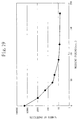
- Figure 8 shows the relation between the grain size of the polysilicon film 43 and the number of particles on the polysilicon film 43 when the time required for plasma processing performed by using the plasma composed of N 2 gas and the grain size are varied.
- the number of particles is counted based on optical reflection obtained when the top surface of the polysilicon film 43 is irradiated with laser light, which is expressed as number/8-inch wafer.
- the number of particles on the polysilicon film 43 is reduced as the grain size of the polysilicon film 43 is reduced from 0.5 ⁇ m to 0.05 ⁇ m. This may be because grains of larger size and an interface therebetween are more rugged, which may be attributed to an increased quantity of S-based residues.
- the number of particles on the polysilicon film 43 can also be reduced by increasing the time required for plasma processing performed by using the plasma composed of N 2 gas from 30 seconds to 90 seconds.
- the S-based residues on the polysilicon film 43 and on the resist pattern 45 can be reduced by increasing the time required for plasma processing performed by using the plasma composed of N 2 gas based on the grain size of the polysilicon film 43 , which in turn reduces the number of particles.
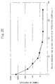
- Figure 9 shows the relation between the grain size of the polysilicon film 43 and the number of particles on the polysilicon film 43 when the pressure of gas and the grain size are varied.
- the number of particles is counted based on optical reflection obtained when the top surface of the polysilicon film 43 is irradiated with laser light, which is expressed as number/8-inch wafer.
- the number of particles on the polysilicon film 43 is reduced as the grain size of the polysilicon film 43 is reduced from 0.5 ⁇ m to 0.05 ⁇ m.
- the number of particles on the polysilicon film 43 can also be reduced by increasing the pressure of N 2 gas during plasma processing from 10 mTorr to 100 mTorr.
- the S-based residues on the polysilicon film 43 and on the resist pattern 45 can be reduced by increasing the pressure of N 2 gas during plasma processing in accordance with the grain size of the polysilicon film 43 and with the ruggedness of the surface of the polysilicon film 43 , which in turn reduces the number of particles.
- Figure 10 shows the relation between the grain size of the polysilicon film 43 and the number of particles on the polysilicon film 43 when the flow rate of N 2 gas and the grain size are varied.
- the number of particles is counted based on optical reflection obtained when the top surface of the polysilicon film 43 is irradiated with laser light, which is expressed as number/8-inch wafer.
- the number of particles on the polysilicon film 43 is reduced as the grain size of the polysilicon film 43 is reduced from 0.5 ⁇ m to 0.05 ⁇ m.
- the number of particles on the polysilicon film 43 can also be reduced by increasing the flow rate of gas during plasma processing composed of N 2 gas from 20 sccm to 80 sccm.
- the S-based residues on the polysilicon film 43 and on the resist pattern 45 can be reduced by increasing the flow rate of N 2 gas during plasma processing in accordance with the grain size of the polysilicon film 43 and with the ruggedness of the surface of the polysilicon film 43 , which in turn reduces the number of particles.
- Figure 11 shows the relation between the grain size of the polysilicon film 43 and the number of particles on the polysilicon film 43 when the temperature of the silicon wafer 41 and the grain size are varied during plasma processing performed by using the plasma composed of N 2 gas.
- the number of particles is counted based on optical reflection obtained when the top surface of the polysilicon film 43 is irradiated with laser light, which is expressed as number/8-inch wafer.
- the number of particles on the polysilicon film 43 is reduced as the grain size of the polysilicon film 43 is reduced from 0.5 ⁇ m to 0.05 ⁇ m.
- the number of particles on the polysilicon film 43 can also be reduced by increasing the temperature of the silicon wafer 41 from -10 °C to 50 °C during plasma processing performed by using the plasma composed of N 2 gas.
- the S-based residues on the polysilicon film 43 and on the resist pattern 45 can be reduced by increasing the temperature of the silicon wafer 41 during plasma processing performed by using the plasma composed of N 2 gas in accordance with the grain size of the polysilicon film 43 and with the ruggedness of the surface of the polysilicon film 43 , which in turn reduces the number of particles.
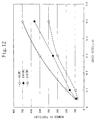
- Figure 12 shows the relation between the grain size of the polysilicon film 43 and the number of particles on the polysilicon film 43 when LEP power and the grain size are varied during plasma processing performed by using the plasma composed of N 2 gas.
- the number of particles is counted based on optical reflection obtained when the top surface of the polysilicon film 43 is irradiated with laser light, which is expressed as number/8-inch wafer.
- the number of particles on the polysilicon film 43 is reduced as the grain size of the polysilicon film 43 is reduced from 0.5 ⁇ m to 0.05 ⁇ m.
- the number of particles on the polysilicon film 43 can also be reduced by increasing LEP power from 50 W to 150 W during plasma processing performed by using the plasma composed of N 2 gas.
- the S-based residues on the polysilicon film 43 and on the resist pattern 45 can be reduced by increasing LEP power during plasma processing performed by using the plasma composed of N 2 gas in accordance with the grain size of the polysilicon film 43 and with the ruggedness of the surface of the polysilicon film 43 , which in turn reduces the number of particles.
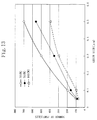
- Figure 13 shows the relation between the grain size of the polysilicon film 43 and the number of particles on the polysilicon film 43 when RF power and the grain size are varied during plasma processing performed by using the plasma composed of N 2 gas.
- the number of particles is counted based on optical reflection obtained when the top surface of the polysilicon film 43 is irradiated with laser light, which is expressed as number/8-inch wafer.
- the number of particles on the polysilicon film 43 is reduced as the grain size of the polysilicon film 43 is reduced from 0.5 ⁇ m to 0.05 ⁇ m.
- the number of particles on the polysilicon film 43 can also be reduced by increasing RF power from 50 W to 150 W during plasma processing performed by using the plasma composed of N 2 gas.
- the S-based residues on the polysilicon film 43 and on the resist pattern 45 can be reduced by increasing RF power during plasma processing performed by using the plasma composed of N 2 gas in accordance with the grain size of the polysilicon film 43 and with the ruggedness of the surface of the polysilicon film 43 , which in turn reduces the number of particles.
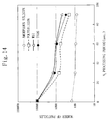
- Figure 14 shows the relation between a plasma processing time and the number of particles on the polysilicon film 43 when plasma processing is performed by using the plasma composed of N 2 gas and different types of underlying films, while varying the processing time.
- the number of particles is counted based on optical reflection obtained when the top surface of the polysilicon film 43 is irradiated with laser light, which is expressed as number/8-inch wafer.
- the number of particles after plasma processing performed by using the plasma composed of N 2 gas is varied with different types of underlying films which are an amorphous silicon film, a polysilicon film, a WSi film, and a TEOS film.
- the number of particles on the underlying film can also be reduced by increasing the plasma processing time from 0 to 90 seconds. In short, the number of particles can be reduced by varying the plasma processing time depending on the type of the underlying film in use.
- the plasma processing time has been used as an example in describing the effect of varying conditions for plasma processing performed by using the plasma composed of N 2 gas depending on the type of the underlying film in use, it will be appreciated that similar effects can be achieved by varying gas pressure, a gas flow rate, LEP power, RF power, the temperature of the silicon wafer 41 , or the like during plasma processing.
- a seventh embodiment performs dry etching with respect to the organic bottom anti-reflective coating by using SO 2 -based etching gas and heats the silicon wafer 41 to evaporate and remove the S component present on the polysilicon film 43 , the resist pattern 45 , and the organic bottom anti-reflective coating 44 .
- the silicon wafer 41 After dry etching is performed with respect to the organic bottom anti-reflective coating 44 by using SO 2 gas, the silicon wafer 41 is placed and heated in a hot plate oven for 1 minute.
- Figure 15 shows the relation between a heating temperature in the hot plate oven and the number of particles on the polysilicon film 43 when the heating temperature is varied.
- the number of particles is counted based on optical reflection obtained when the top surface of the polysilicon film 43 is irradiated with laser light, which is expressed as number/8-inch wafer.
- the number of particles on the polysilicon film 43 is reduced as the heating temperature is increased from 30 °C.
- the number of particles is reduced significantly when the heating temperature becomes 70 °C or higher.
- the resist pattern 45 is deformed when the heating temperature becomes 120 °C or higher, so that the heating temperature is preferably in the range of 70 to 120 °C. Since the number of particles is 10 or less and barely varies when the heating temperature becomes 120 °C or higher, a particularly preferred heating temperature is on the order of 100 °C.
- Figure 16 shows the relationship between a heating time and the number of particles on the polysilicon film 43 when the silicon wafer 41 is heated in a hot plate oven at 100 °C.
- the number of particles is counted based on optical reflection obtained when the top surface of the polysilicon film 43 is irradiated with laser light, which is expressed as number/8-inch wafer.
- the number of particles is reduced as the heating time is increased from 0 to 60 seconds.
- the number of particles is 10 or less and barely varies when the heating time becomes 60 seconds or longer.
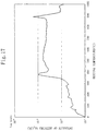
- Figure 17 shows the relation between a heating temperature and the intensity of a SO 2 component detected by TDS (Thermal Desorption mass Spectroscopy), i.e., the relation between the heating temperature and the desorption of the S component.
- TDS Thermal Desorption mass Spectroscopy
- the amount of discharged SO 2 is increased as the heating temperature is increased at the heating temperature ranging from 0 to 300 °C, though there are slight variations.
- An eight embodiment performs dry etching with respect to the organic bottom anti-reflective coating by using SO 2 -based etching gas and then washes the silicon 41 with warm water, thereby removing residues having the S component present on the polysilicon film 43 , the resist pattern 45 , and the organic bottom anti-reflective coating 44 .
- the silicon wafer 41 After dry etching is performed with respect to the organic bottom anti-reflective coating 44 by using SO 2 gas, the silicon wafer 41 is washed in a washing bath for 90 seconds.
- Figure 18 shows the relation between the temperature of washing water and the number of particles on the polysilicon film 43 when the temperature of washing water is varied.
- the number of particles is counted based on optical reflection obtained when the top surface of the polysilicon film 43 is irradiated with laser light, which is expressed as number/8-inch wafer.
- the number of particles on the polysilicon film 43 is reduced as the temperature of washing water is increased from 20 °C to 100 °C. However, since water boils at 100 °C, washing should be performed at a temperature of 90 °C or lower.
- Figure 19 shows the relation between a washing time and the number of particles on the polysilicon film 43 when the silicon wafer 41 is washed in the washing bath at 70 °C.
- the number of particles is counted based on optical reflection obtained when the top surface of the polysilicon film 43 is irradiated with laser light, which is expressed as number/8-inch wafer.
- the number of particles is reduced as the washing time is increased from 0 to 120 seconds.
- the number of particles is 10 or less and barely varies when the washing time becomes 120 seconds or longer.
- a ninth embodiment performs dry etching with respect to the organic bottom anti-reflective coating by using SO 2 etching gas, neutralizes acidic residues containing sulfuric acid as the main component and remaining on the silicon wafer 41 with an alkaline developing solution for lithography, and washes away the developing solution to thereby remove the residues having the S component present on the polysilicon film 43, the resist pattern 45 , and the organic bottom anti-reflective coating 44 .
- Figure 20 shows the relation between a neutralization time and the number of particles on the polysilicon film 43 when the residues containing sulfuric acid as the main component are neutralized with the developing solution at 22 °C.
- the number of particles is counted based on optical reflection obtained when the top surface of the polysilicon film 43 is irradiated with laser light, which is expressed as number/8-inch wafer.
- the number of particles on the polysilicon film 43 is reduced as the developing time is increased from 0 to 120 seconds. However, the number of particles is 10 or less and barely varies when the developing time becomes 120 seconds or longer.
- each of the fifth to ninth embodiments has used the polysilicon film 43 as the underlying film for the organic bottom anti-reflective coating 44 , it will be appreciated that similar effects can also be achieved in the case where the underlying film is composed of an oxide film such as TEOS, a nitride film, a tungsten silicide film, a metal alloy film, a ferroelectric film, or the like in the step of removing the remaining S component resulting from dry etching previously performed by using etching gas containing gas having the S component.
- oxide film such as TEOS, a nitride film, a tungsten silicide film, a metal alloy film, a ferroelectric film, or the like
- each of the first to ninth embodiments has used the first dry-etching apparatus in accordance with the LEP (Lissajous Electron Plasma) system shown in Figure 2 , it will be appreciated that similar effects can also be achieved even when a dry-etching apparatus having a plasma source in accordance with RIE (Reactive Ion Etching), ECR (Electron Cyclotron Resonance), ICP (Inductive Coupled Plasma), TCP (Transformer Coupled Plasma) or like system is used.
- RIE Reactive Ion Etching
- ECR Electrode
- ICP Inductive Coupled Plasma
- TCP Transformer Coupled Plasma
- a tenth embodiment has been achieved based on the foregoing second knowledge. Specifically, the tenth embodiment performs dry etching with respect to the organic bottom anti-reflective coating 44 containing silicon by using Cl 2 /O 2 -based etching gas containing halogen as the main component. As a result of analysis, it was found that the material of the organic bottom anti-reflective coating (CD9TM commercially available from Brewer Science Co., U.S.A.) used in the tenth embodiment had about 10 ppm of silicon mixed therein.
- CD9TM commercially available from Brewer Science Co., U.S.A.
- Etching properties are as shown in Table 21 .
- the organic bottom anti-reflective coating exhibited vertical profiles, though there are slight variations in the size of the organic bottom anti-reflective coating 44 .
- foreign residues generated by conventional dry etching using N 2 /O 2 gas was no more generated.
- the reason for no foreign residue may be that silicon contained in the organic bottom anti-reflective coating 44 is etched by Cl radicals contained in Cl 2 /O 2 -based etching gas and there is no unreacted silicon component left.
- an eleventh embodiment has also been achieved based on the foregoing second knowledge. Specifically, the eleventh embodiment performs dry etching with respect to the organic bottom anti-reflective coating 44 by using etching gas composed of Cl 2 /O 2 -based etching gas with SO 2 gas added thereto.
- the eleventh embodiment has also used the material of the organic bottom anti-reflective coating (CD9TM commercially available from Brewer Science Co., U.S.A.).
- the eleventh embodiment has also used the second dry etching apparatus shown in Figure 3 and the film having the structure shown in Figure 4 as a target film, similarly to the tenth embodiment.
- the organic bottom anti-reflective coating 44 was slightly smaller in size than the resist pattern 45
- the slight variations were further reduced in the eleventh embodiment.
- the organic bottom anti-reflective coating 44 is smaller in size than the resist pattern 45
- the size of a pattern formed by etching the polysilicon film 43 masked with the resist pattern 45 and with the organic bottom anti-reflective coating 44 varies disadvantageously.
- the reason for no foreign residue in the eleventh embodiment may be that silicon contained in the organic bottom anti-reflective coating 44 is etched by Cl radicals contained in Cl 2 /O 2 /SO 2 -based etching gas and there is no unreacted silicon component left.
- the reason for reduced variations in the size of the organic bottom anti-reflective coating 44 may be the difficulty with which C as the main component of each of the resist pattern 45 and the organic bottom anti-reflective coating 44 reacts with S as the etchant to form CS 2 gas. Consequently, sidewall protecting films in the form of a polymer having C-S bonds are more likely to be attached to the respective sidewalls of the resist pattern 43 and the organic bottom anti-reflective coating 44 , which suppresses a reduction in the size of the organic bottom anti-reflective coating 44 .
- a twelfth embodiment performs a dry-etching step with respect to the organic bottom anti-reflective coating containing silicon by using etching gas composed of Cl 2 /SO 2 /O 2 gas and then plasma processing by using N 2 gas which is inert gas containing no S component.
- the twelfth embodiment has also used the material of the organic bottom anti-reflective coating (CD9TM commercially available from Brewer Science Co., U.S.A.).
- the twelfth embodiment has also used the second dry etching apparatus shown in Figure 3 and the film having the structure shown in Figure 4 as a target film.
- the result of quantitative analysis of S carried out by ion chromatography was 160 ⁇ g/8-inch wafer in the case where only the step (1) was performed, i.e., where only dry etching was performed with respective to the organic bottom anti-reflective coating 44 by using etching gas composed of Cl 2 /SO 2 /O 2 gas.
- the result of quantitative analysis of S carried out by ion chromatography was 30 ⁇ g/8-inch wafer in the case where the steps of (1) and (2) were performed, i.e., where dry etching was performed with respect to the organic bottom anti-reflective coating 44 by using etching gas composed of Cl 2 /SO 2 /O 2 gas and then plasma processing was performed by using a plasma composed of N 2 gas without applying a bias voltage to the sample stage 23 as the lower electrode holding the silicon wafer 41 as a target material.
- the amount of S was reduced significantly in the case where the steps (1) and (2) were performed.
- etching gas contains the S component in the twelfth embodiment, the S component remains on the silicon wafer 41 after dry etching performed with respect to the organic bottom anti-reflective coating 44 .
- the remaining S component may react with moisture contained in the atmosphere to generate residues.
- plasma processing is performed by using N 2 gas with a bias voltage being applied to the sample stage 23 holding the silicon wafer 41 , it is effective in reducing the remaining S component but a pattern collapse may occur in the upper portion of the resist pattern 45 . This may be attributed to an excessive amount of N + ion component present in the upper portion of the resist pattern 45 , which sputters the upper portion of the resist pattern 45 .
- the twelfth embodiment has performed plasma processing by using N 2 gas without applying a bias voltage to the sample stage 23 , it is also possible to perform anode-coupling plasma processing instead.
- the dry-etching step has been performed by using etching gas containing the S component
- plasma processing is performed by using a plasma composed of N 2 gas containing no S component in the twelfth embodiment. Therefore, the conditions for plasma processing used in the twelfth embodiment, particularly for plasma processing performed without applying a bias voltage to the sample stage 23 and plasma processing performed by the anode coupling system, are also applicable to plasma processing performed in the fifth or sixth embodiment.
- each of the tenth to twelfth embodiments has used the second dry-etching apparatus in accordance with the ICP (Inductively Coupled Plasma) shown in Figure 3 , it will be appreciated that similar effects can also be achieved even when a dry-etching apparatus having a plasma source in accordance with RIE (Reactive Ion Etching), ECR (Electron Cyclotron Resonance), TCP (Transformer Coupled Plasma), LEP (Lissajous Electron Plasma), or like system is used.
- RIE Reactive Ion Etching
- ECR Electrode Coupled Plasma
- TCP Transformer Coupled Plasma
- LEP Lisajous Electron Plasma
Landscapes
- Engineering & Computer Science (AREA)
- Architecture (AREA)
- Structural Engineering (AREA)
- Physics & Mathematics (AREA)
- General Physics & Mathematics (AREA)
- Drying Of Semiconductors (AREA)
Applications Claiming Priority (7)
| Application Number | Priority Date | Filing Date | Title |
|---|---|---|---|
| JP825397 | 1997-01-21 | ||
| JP8253/97 | 1997-01-21 | ||
| JP189579/97 | 1997-07-15 | ||
| JP18958197 | 1997-07-15 | ||
| JP189581/97 | 1997-07-15 | ||
| JP18957997 | 1997-07-15 | ||
| PCT/JP1997/004455 WO1998032162A1 (en) | 1997-01-21 | 1997-12-04 | Pattern forming method |
Publications (2)
| Publication Number | Publication Date |
|---|---|
| EP0903777A1 true EP0903777A1 (de) | 1999-03-24 |
| EP0903777A4 EP0903777A4 (de) | 2005-09-14 |
Family
ID=27277946
Family Applications (1)
| Application Number | Title | Priority Date | Filing Date |
|---|---|---|---|
| EP97946114A Withdrawn EP0903777A4 (de) | 1997-01-21 | 1997-12-04 | Musterformverfahren |
Country Status (4)
| Country | Link |
|---|---|
| US (1) | US6187688B1 (de) |
| EP (1) | EP0903777A4 (de) |
| CN (1) | CN1107342C (de) |
| WO (1) | WO1998032162A1 (de) |
Cited By (7)
| Publication number | Priority date | Publication date | Assignee | Title |
|---|---|---|---|---|
| DE19939317A1 (de) * | 1999-08-19 | 2001-02-22 | Bosch Gmbh Robert | Verfahren zur Herstellung von Polymerstrukturen mittels eines Ätzprozesses |
| WO2002029879A1 (de) * | 2000-10-04 | 2002-04-11 | Infineon Technologies Ag | Verfahren zum ätzen von organischen antireflexionsschichten |
| US6849389B2 (en) * | 2001-07-12 | 2005-02-01 | International Business Machines Corporation | Method to prevent pattern collapse in features etched in sulfur dioxide-containing plasmas |
| WO2006107495A1 (en) * | 2005-03-30 | 2006-10-12 | Lam Research Corporation | Etch profile control |
| US8158524B2 (en) | 2007-09-27 | 2012-04-17 | Lam Research Corporation | Line width roughness control with arc layer open |
| US8501627B2 (en) | 2007-09-27 | 2013-08-06 | Lam Research Corporation | Profile control in dielectric etch |
| KR20150034660A (ko) * | 2013-09-26 | 2015-04-03 | 램 리써치 코포레이션 | 조합형 마스크를 이용한 고 애스팩트 비 에칭 |
Families Citing this family (23)
| Publication number | Priority date | Publication date | Assignee | Title |
|---|---|---|---|---|
| JP3955385B2 (ja) * | 1998-04-08 | 2007-08-08 | Azエレクトロニックマテリアルズ株式会社 | パターン形成方法 |
| US6383941B1 (en) * | 2000-07-06 | 2002-05-07 | Applied Materials, Inc. | Method of etching organic ARCs in patterns having variable spacings |
| US6617257B2 (en) | 2001-03-30 | 2003-09-09 | Lam Research Corporation | Method of plasma etching organic antireflective coating |
| JP2005508078A (ja) * | 2001-10-31 | 2005-03-24 | 東京エレクトロン株式会社 | 高アスペクト比形態のエッチング方法 |
| US6649532B1 (en) * | 2002-05-09 | 2003-11-18 | Applied Materials Inc. | Methods for etching an organic anti-reflective coating |
| JP3913145B2 (ja) * | 2002-08-28 | 2007-05-09 | 松下電器産業株式会社 | パターン形成方法 |
| JP4034164B2 (ja) * | 2002-10-28 | 2008-01-16 | 富士通株式会社 | 微細パターンの作製方法及び半導体装置の製造方法 |
| US7119020B2 (en) | 2002-12-04 | 2006-10-10 | Matsushita Electric Industrial Co., Ltd. | Method for fabricating semiconductor device |
| US6972255B2 (en) * | 2003-07-28 | 2005-12-06 | Freescale Semiconductor, Inc. | Semiconductor device having an organic anti-reflective coating (ARC) and method therefor |
| US7176130B2 (en) * | 2004-11-12 | 2007-02-13 | Freescale Semiconductor, Inc. | Plasma treatment for surface of semiconductor device |
| KR100685903B1 (ko) * | 2005-08-31 | 2007-02-26 | 동부일렉트로닉스 주식회사 | 반도체 소자의 제조 방법 |
| WO2008137670A1 (en) * | 2007-05-03 | 2008-11-13 | Lam Research Corporation | Hardmask open and etch profile control with hardmask open |
| CN101925984A (zh) * | 2008-02-01 | 2010-12-22 | 朗姆研究公司 | 减小光阻剥离过程中对低k材料的损害 |
| US8133819B2 (en) | 2008-02-21 | 2012-03-13 | Applied Materials, Inc. | Plasma etching carbonaceous layers with sulfur-based etchants |
| US8394722B2 (en) * | 2008-11-03 | 2013-03-12 | Lam Research Corporation | Bi-layer, tri-layer mask CD control |
| JP5606060B2 (ja) | 2009-12-24 | 2014-10-15 | 東京エレクトロン株式会社 | エッチング方法及びエッチング処理装置 |
| JP2013222852A (ja) * | 2012-04-17 | 2013-10-28 | Tokyo Electron Ltd | 有機膜をエッチングする方法及びプラズマエッチング装置 |
| US9105587B2 (en) | 2012-11-08 | 2015-08-11 | Micron Technology, Inc. | Methods of forming semiconductor structures with sulfur dioxide etch chemistries |
| JP6185305B2 (ja) * | 2013-06-28 | 2017-08-23 | 東京エレクトロン株式会社 | プラズマエッチング方法およびプラズマエッチング装置 |
| CN106096087B (zh) * | 2016-05-31 | 2019-08-13 | 上海华虹宏力半导体制造有限公司 | 占领图形填充方法 |
| US10242883B2 (en) | 2017-06-23 | 2019-03-26 | Lam Research Corporation | High aspect ratio etch of oxide metal oxide metal stack |
| CN115066742B (zh) * | 2020-02-19 | 2025-09-30 | 东京毅力科创株式会社 | 基片处理方法和基片处理系统 |
| JP7482586B1 (ja) * | 2023-08-07 | 2024-05-14 | 株式会社トッパンフォトマスク | フォトマスク及びその検査方法 |
Family Cites Families (14)
| Publication number | Priority date | Publication date | Assignee | Title |
|---|---|---|---|---|
| JPS6077429A (ja) * | 1983-10-04 | 1985-05-02 | Asahi Glass Co Ltd | ドライエツチング方法 |
| JPH01307227A (ja) * | 1988-06-06 | 1989-12-12 | Showa Denko Kk | 微細加工方法 |
| DE68923247T2 (de) * | 1988-11-04 | 1995-10-26 | Fujitsu Ltd | Verfahren zum Erzeugen eines Fotolackmusters. |
| FR2673763A1 (fr) * | 1991-03-06 | 1992-09-11 | Centre Nat Rech Scient | Procede de gravure anisotrope des polymeres par plasma. |
| JPH04338630A (ja) * | 1991-05-15 | 1992-11-25 | Mitsubishi Electric Corp | 半導体装置の製造方法 |
| JPH06138664A (ja) * | 1992-10-26 | 1994-05-20 | Mitsubishi Electric Corp | パターン形成方法 |
| JPH07263425A (ja) * | 1994-03-25 | 1995-10-13 | Sony Corp | 積層配線のドライエッチング方法 |
| JP3353490B2 (ja) * | 1994-10-12 | 2002-12-03 | ソニー株式会社 | 積層配線のパターニング方法 |
| JP2674589B2 (ja) * | 1995-11-09 | 1997-11-12 | 日本電気株式会社 | レジストパターンの形成方法 |
| US5804088A (en) * | 1996-07-12 | 1998-09-08 | Texas Instruments Incorporated | Intermediate layer lithography |
| KR100232187B1 (ko) * | 1996-12-27 | 1999-12-01 | 김영환 | 반사방지막 식각방법 |
| JPH10242127A (ja) * | 1997-02-26 | 1998-09-11 | Sony Corp | 有機系反射防止膜のプラズマエッチング方法 |
| JPH10261618A (ja) * | 1997-03-18 | 1998-09-29 | Sony Corp | 有機系反射防止膜のエッチング方法 |
| JPH10312993A (ja) * | 1997-05-12 | 1998-11-24 | Sony Corp | 有機系反射防止膜のプラズマエッチング方法 |
-
1997
- 1997-12-04 CN CN97192931A patent/CN1107342C/zh not_active Expired - Fee Related
- 1997-12-04 US US09/142,252 patent/US6187688B1/en not_active Expired - Fee Related
- 1997-12-04 WO PCT/JP1997/004455 patent/WO1998032162A1/ja not_active Ceased
- 1997-12-04 EP EP97946114A patent/EP0903777A4/de not_active Withdrawn
Cited By (9)
| Publication number | Priority date | Publication date | Assignee | Title |
|---|---|---|---|---|
| DE19939317A1 (de) * | 1999-08-19 | 2001-02-22 | Bosch Gmbh Robert | Verfahren zur Herstellung von Polymerstrukturen mittels eines Ätzprozesses |
| EP1077124A3 (de) * | 1999-08-19 | 2001-08-01 | Robert Bosch Gmbh | Verfahren zur Herstellung von Polymerstrukturen mittels eines Ätzprozesses |
| WO2002029879A1 (de) * | 2000-10-04 | 2002-04-11 | Infineon Technologies Ag | Verfahren zum ätzen von organischen antireflexionsschichten |
| US6849389B2 (en) * | 2001-07-12 | 2005-02-01 | International Business Machines Corporation | Method to prevent pattern collapse in features etched in sulfur dioxide-containing plasmas |
| WO2006107495A1 (en) * | 2005-03-30 | 2006-10-12 | Lam Research Corporation | Etch profile control |
| US7645707B2 (en) | 2005-03-30 | 2010-01-12 | Lam Research Corporation | Etch profile control |
| US8158524B2 (en) | 2007-09-27 | 2012-04-17 | Lam Research Corporation | Line width roughness control with arc layer open |
| US8501627B2 (en) | 2007-09-27 | 2013-08-06 | Lam Research Corporation | Profile control in dielectric etch |
| KR20150034660A (ko) * | 2013-09-26 | 2015-04-03 | 램 리써치 코포레이션 | 조합형 마스크를 이용한 고 애스팩트 비 에칭 |
Also Published As
| Publication number | Publication date |
|---|---|
| CN1107342C (zh) | 2003-04-30 |
| EP0903777A4 (de) | 2005-09-14 |
| CN1213456A (zh) | 1999-04-07 |
| US6187688B1 (en) | 2001-02-13 |
| WO1998032162A1 (en) | 1998-07-23 |
Similar Documents
| Publication | Publication Date | Title |
|---|---|---|
| US6187688B1 (en) | Pattern formation method | |
| US6759286B2 (en) | Method of fabricating a gate structure of a field effect transistor using a hard mask | |
| US6322714B1 (en) | Process for etching silicon-containing material on substrates | |
| US6924191B2 (en) | Method for fabricating a gate structure of a field effect transistor | |
| US7431795B2 (en) | Cluster tool and method for process integration in manufacture of a gate structure of a field effect transistor | |
| US5980768A (en) | Methods and apparatus for removing photoresist mask defects in a plasma reactor | |
| US6767824B2 (en) | Method of fabricating a gate structure of a field effect transistor using an alpha-carbon mask | |
| US20050085090A1 (en) | Method for controlling accuracy and repeatability of an etch process | |
| KR20010032030A (ko) | 자체 세정가능한 에칭 공정 | |
| KR20010032913A (ko) | 기판으로부터의 유기성 반사 방지 코팅 에칭 시스템 및 방법 | |
| JP2006522480A (ja) | 多層フォトレジストのドライ現像のための方法及び装置 | |
| US20040237997A1 (en) | Method for removal of residue from a substrate | |
| WO1997045866A1 (en) | Mechanism for uniform etching by minimizing effects of etch rate loading | |
| WO2009079284A1 (en) | Method and system for reducing line edge roughness during pattern etching | |
| KR100595090B1 (ko) | 포토레지스트 마스크를 사용한 개선된 엣칭방법 | |
| JP4594235B2 (ja) | Arc層をエッチングする方法 | |
| CN101263582A (zh) | 用于利用基于sf6的化学物质刻蚀掺杂硅的方法和系统 | |
| KR20000071381A (ko) | 드라이 에칭 방법 및 반도체 장치의 제조 방법 | |
| US6027959A (en) | Methods for in-situ removal of an anti-reflective coating during a nitride resistor protect etching process | |
| KR20000057897A (ko) | 지정된 기판 상에 놓여져 있는 패턴화된 마스크 표면 위로조립 구조물을 증착하기 위한 방법 | |
| US6066567A (en) | Methods for in-situ removal of an anti-reflective coating during an oxide resistor protect etching process | |
| US7344991B2 (en) | Method and apparatus for multilayer photoresist dry development | |
| JP2928391B2 (ja) | パターン形成方法 | |
| US8048325B2 (en) | Method and apparatus for multilayer photoresist dry development | |
| CN100452300C (zh) | 多晶硅栅极蚀刻后的无机抗反射涂层的干式各向同性移除 |
Legal Events
| Date | Code | Title | Description |
|---|---|---|---|
| PUAI | Public reference made under article 153(3) epc to a published international application that has entered the european phase |
Free format text: ORIGINAL CODE: 0009012 |
|
| 17P | Request for examination filed |
Effective date: 19980825 |
|
| AK | Designated contracting states |
Kind code of ref document: A1 Designated state(s): DE FR GB NL |
|
| RIC1 | Information provided on ipc code assigned before grant |
Ipc: 7H 01L 21/3213 B Ipc: 7H 01L 21/311 B Ipc: 7G 03F 7/26 B Ipc: 7H 01L 21/302 A |
|
| A4 | Supplementary search report drawn up and despatched |
Effective date: 20050728 |
|
| 17Q | First examination report despatched |
Effective date: 20061122 |
|
| STAA | Information on the status of an ep patent application or granted ep patent |
Free format text: STATUS: THE APPLICATION HAS BEEN WITHDRAWN |
|
| 18W | Application withdrawn |
Effective date: 20080411 |