糸田 » パターン形成方法 Itoda »Pattern formation method
【技術分野】 【Technical field】
本発明は、 レジスト膜よりなるレジストパターンを形成するパターン形成方法 に関し、 特に、 レジスト膜の下に堆積された有機系反射防止膜に対してレジスト パターンをマスクとしてドライエッチングを行なう技術に関する。 The present invention relates to a pattern forming method for forming a resist pattern made of a resist film, and more particularly to a technique for performing dry etching on an organic antireflection film deposited under the resist film using the resist pattern as a mask.
【背景技術】 [Background Art]
近年、 半導体集積回路素子の微細化に伴って、 リソグラフィー工程における露 光光の光源は短波長化しており、 現在では、 光源としては K r Fエキシマレ一ザ (波長 248 nm) 等が用いられようとしている。 In recent years, the light source of the exposure light in the lithography process has been shortened with the miniaturization of semiconductor integrated circuit elements, and a KrF excimer laser (wavelength: 248 nm) etc. will be used as the light source at present. And
ところで、 露光光の光源が短波長化すればするほど、 レジスト膜に対して露光 を行なう際の露光光の基板反射率が増加するため、 露光光が基板で反射されてな る反射光に起因するレジストパターンの寸法変動が起きやすい。 レジストパター ンの寸法変動は、 露光光がレジスト膜の下の基板で反射されて、 反射光としてレ ジスト膜に入射する際に、 レジスト膜が反射光により再び露光されてしまうため 、 レジスト膜における露光したくない部分まで露光されることにより発生する。 そこで、 最近では、 反射光のレジス卜膜への入射を抑制するために、 レジスト 膜の下に有機系反射防止膜 (Organic Bottom Anti-Reflective Coating :以下、 各表及び図面においては、 単に ARCと略する。 ) を形成するプロセスが提案さ れている。 このプロセスは、 主として、 ゲ一卜幅が 0. 25 m以下のルールを 持つ高性能デバイスにおける半導体素子の製造工程において用いられる技術であ る。 By the way, as the light source of the exposure light becomes shorter, the substrate reflectance of the exposure light at the time of exposing the resist film increases, and the exposure light is caused by the reflected light that is reflected by the substrate. The size of the resist pattern changes easily. The dimensional fluctuation of the resist pattern is caused by the fact that when the exposure light is reflected by the substrate below the resist film and is incident on the resist film as reflected light, the resist film is exposed again by the reflected light. This is caused by exposing a portion that is not desired to be exposed. Therefore, recently, in order to suppress the incidence of reflected light on the resist film, an organic antireflective coating (Organic Bottom Anti-Reflective Coating: below) is simply referred to as ARC in each of the tables and drawings below the resist film. A process for forming) has been proposed. This process is mainly used in the manufacturing process of semiconductor devices in high-performance devices having a rule of 0.25 m or less in gate width.
以下、 図 1 (a) 〜 (e) を参照にしながら、 有機系反射防止膜を利用したレ ジス卜パターンの形成方法について説明する。 Hereinafter, a method of forming a resist pattern using an organic antireflection film will be described with reference to FIGS. 1 (a) to 1 (e).
まず、 図 1 (a) に示すように、 下地膜 1 1 (例えば、 ポリシリコン膜、 シリ コン酸化膜又はタングステンシリサイ ド膜) 上に、 表面が平坦になるように有機 系反射防止膜 1 2を堆積した後、 図 1 (b) に示すように、 有機系反射防止膜 1
2の上に、 ポジ型のレジス卜よりなるレジスト膜 1 3を堆積する。 First, as shown in FIG. 1 (a), an organic antireflection film 1 is formed on a base film 11 (for example, a polysilicon film, a silicon oxide film or a tungsten silicide film) so that the surface becomes flat. After depositing 2, organic anti-reflective coating 1 as shown in Fig. 1 (b) On top of the resist film 2, a resist film 13 made of a positive resist is deposited.
次に、 図 1 (c) に示すように、 マスク 14を用いてレジスト膜 1 3に対して 選択的に露光を行なった後、 露光されたレジスト膜 1 3に対して現像処理を行な うことにより、 図 1 (d) に示すように、 レジスト膜 1 3における露光部を除去 して、 レジス卜パターン 1 5を形成する。 Next, as shown in FIG. 1C, after selectively exposing the resist film 13 using the mask 14, the exposed resist film 13 is developed. Thus, as shown in FIG. 1D, the exposed portions of the resist film 13 are removed to form a resist pattern 15.
次に、 図 1 (e) に示すように、 レジストパターン 1 5をマスクとして有機系 反射防止膜 1 2に対してドライエッチングを行なって、 有機系反射防止膜 1 2に おけるレジストパターン 1 5に覆われていない部分を除去する。 Next, as shown in FIG. 1 (e), dry etching is performed on the organic anti-reflection film 12 using the resist pattern 15 as a mask to form a resist pattern 15 on the organic anti-reflection film 12. Remove the uncovered parts.
ところで、 前記のように有機系反射防止膜 1 2を用いるパターン形成方法にお いては、 有機系反射防止膜 1 2に対してドライエッチングを行なう際に、 有機系 反射防止膜 1 2に寸法変動が発生し易いという問題、 有機系反射防止膜 1 2とシ リコンを含む下地膜 1 1との選択比が低いという問題、 及び、 エッチングを行な う反応室内に発生するパーティクルが増加するという問題がある。 By the way, in the pattern forming method using the organic anti-reflection film 12 as described above, when dry etching is performed on the organic anti-reflection film 12, the dimensional fluctuation of the organic anti-reflection film 12 is caused. Problem that the organic antireflection film 12 and the underlying film 11 containing silicon are low in selectivity, and the problem that particles generated in the reaction chamber where etching is performed increases. There is.
有機系反射防止膜 1 2に寸法変動が発生し易いという問題については、 有機系 反射防止膜 1 2がレジスト膜 1 3と同様に力一ボン系の材料であるため、 有機系 反射防止膜 1 2をエッチングする際にレジストパターン 1 5も同時にエッチング されてしまうことが原因であると考えられる。 Regarding the problem that dimensional fluctuations easily occur in the organic anti-reflection film 12, the organic anti-reflection film 1 is made of a carbon-based material like the resist film 13. It is considered that the reason is that the resist pattern 15 is also etched at the same time when 2 is etched.
また、 反応室内に発生するパーティクルが増加するという問題については、 有 機系反射防止膜 1 2をエッチングする際に、 該有機系反射防止膜 1 2から発生す るパーティクルが原因であると考えられる。 Further, the problem of increasing particles generated in the reaction chamber is considered to be caused by particles generated from the organic anti-reflection film 12 when the organic anti-reflection film 12 is etched. .
そこで、 前記の各問題を解決するため、 有機系反射防止膜 1 2に対するエッチ ングガスとして、 H B r ZOa 系のガス及び N 2 θ 2 系のガスが提案されてい る。 Therefore, in order to solve the above-mentioned problems, HBr ZOa-based gas and N 2 θ 2 -based gas have been proposed as etching gases for the organic anti-reflection film 12.
また、 最近では、 1 996年秋季第 57回応用物理学術講演会において、 有機 系反射防止膜 1 2に対するエッチングガスとして C 12 〇2 系のガスを用いる と、 寸法制御性が良くなると共に下地膜であるポリシリコン膜との選択比も無限 大になると報告されている (NEC :西沢ら、 No.2 p483 7a- T-1) と共に、 有機 系反射防止膜 12に対するエッチングガスとして C OZN 2 /02 系のガスを用 いると、 レジスト膜に対する選択比が向上すると報告されている (LGSemicon Je
onら、 No.2 p522> 8a-T-7) 。 Under Recently, in 1 996 Autumn 57th Applied Physics Scientific Lecture, the use of C 1 2 〇 2 based gas as an etching gas for the organic antireflection film 1 2, the dimensional controllability is improved It has been reported that the selectivity to the polysilicon film, which is the ground film, is also infinite (NEC: Nishizawa et al., No. 2, p483 7a-T-1), and COZN 2 is used as an etching gas for the organic antireflection film 12. It is use the / 0 2 based gas, selectivity to the resist film has been reported to improve (LGSemicon Je on et al., No. 2 p522> 8a-T-7).
(C 1 2 /Oz 系のガスを用いてドライエッチングを行なう場合の問題) ところが、 本件発明者等が、 C 1 2 /02 系のガスを用いて有機系反射防止膜 1 2に対してドライエッチングを行なったところ、 以下に説明するような新たな 問題が生じた。 ' (C 1 2 / Oz system issues when performing dry etching using a gas), however, the present inventors have found the organic antireflection film 1 2 with C 1 2/0 2 based gas Dry etching has created new problems as described below. '
以下、 C 1 /02 系のガスを用いて有機系反射防止膜に対して行なう ドライ エッチング方法について説明する。 ドライエッチング装置としては、 様々なエツ チング装置を用いることができるが、 ここでは、 図 2に示す第 1のエッチング装 置を用いてドライエッチングを行なった場合の結果について説明する。 Hereinafter, a dry etching method performed on an organic antireflection film using a C 1/2 / 2 gas will be described. Various etching apparatuses can be used as the dry etching apparatus. Here, the results when dry etching is performed using the first etching apparatus shown in FIG. 2 will be described.
第 1のエッチング装置は、 接地されていると共に、 内壁面がセラミック、 アル ミナ又は石英等の絶縁物で覆われているチャンバ一 2 1を備えている。 The first etching apparatus is provided with a chamber 21 which is grounded and whose inner wall surface is covered with an insulator such as ceramic, alumina or quartz.
チャンバ一 2 1の内部における側方には、 第 1の側方電極 22A、 第 2の側方 電極 22 B及び第 3の側方電極 22 Cが同一円周上に等間隔に設けられており、 これら第 1の側方電極 22A、 第 2の側方電極 22 B及び第 3の側方電極 22 C には、 第 1の高周波電源 23 A、 第 2の高周波電源 23 B及び第 3の高周波電源 23 Cから放電電力は等しいが位相が互いにほぼ 1 20° づっ異なる 54. 24 MHzの高周波電力が図示しない整合回路を介して供給される。 すなわち、 第 2 の側方電極 2 2 Bには第 1の側方電極 22 Aに比べて位相が 1 20° 進んだ高周 波電力が供給され、 第 3の側方電極 22 Cには第 1の側方電極 22 Aに比べて位 相が 1 20° 遅れた高周波電力が供給される。 尚、 第 1〜第 3の高周波電源 23 A〜23 Cには、 図示しないフェーズシフ夕により 1 20° づつの位相差が生じ る。 · A first side electrode 22A, a second side electrode 22B, and a third side electrode 22C are provided at equal intervals on the same circumference on the side inside the chamber 21. The first side electrode 22A, the second side electrode 22B, and the third side electrode 22C have a first high-frequency power source 23A, a second high-frequency power source 23B, and a third high-frequency power source 23B. A high-frequency power of 54.24 MHz is supplied from a power supply 23 C via a matching circuit (not shown) in which the discharge powers are equal but the phases are different from each other by approximately 120 °. That is, high-frequency power whose phase is advanced by 120 ° compared to the first side electrode 22A is supplied to the second side electrode 22B, and the third side electrode 22C is connected to the second side electrode 22C. High-frequency electric power whose phase is delayed by 120 ° compared to the side electrode 22A of 1 is supplied. The first to third high-frequency power supplies 23A to 23C have a phase difference of 120 ° due to a phase shifter (not shown). ·
チャンバ一 2 1の内部における底部には、 アース電極 24が設けられ、 該ァー ス電極 24の上には、 基板を載置するための下部電極としての試料台 25が設け られている。 試料台 25には第 4の高周波電源 26からバイアス高周波電圧が印 加される。 A ground electrode 24 is provided at the bottom inside the chamber 21, and a sample table 25 as a lower electrode for mounting a substrate is provided on the ground electrode 24. A bias high frequency voltage is applied to the sample table 25 from a fourth high frequency power supply 26.
また、 図示は省略しているが、 チャンバ一 2 1には、 エッチングガスをマスフ 口一コントローラを介してチャンバ一 2 1内に導入するためのガス導入部が設け られていると共に、 チャンバ一 2 1内の圧力を 0. 1 P a〜 1 0 P a程度に制御
するターボポンプが設けられている。 Although not shown, the chamber 21 is provided with a gas introduction unit for introducing an etching gas into the chamber 21 via a mass flow controller, and the chamber 21 is provided with a gas introduction unit. Control the pressure in 1 to about 0.1 Pa to 10 Pa A turbo pump is provided.
以下、 第 1のエッチング装置を用いて行なう有機系反射防止膜に対するドライ エッチング方法について、 図 4 (a) 、 (b) を参照しながら説明する。 Hereinafter, a dry etching method for an organic antireflection film performed using the first etching apparatus will be described with reference to FIGS. 4 (a) and 4 (b).
まず、 図 4 (a) に示すように、 シリコンウェハ 41の上に熱シリコン酸化膜 42を形成した後、 該熱シリコン酸化膜 42の上に下地膜としてのポリシリコン 膜 43を堆積する。 その後、 ポリシリコン膜 43の上に膜厚 1 50 nmの有機系 反射防止膜 44及びレジスト膜を順次堆積した後、 該レジスト膜に対してエッチ ングを行なってレジスト膜よりなるレジストパターン 45を形成する。 First, as shown in FIG. 4A, after a thermal silicon oxide film 42 is formed on a silicon wafer 41, a polysilicon film 43 as a base film is deposited on the thermal silicon oxide film 42. Thereafter, an organic antireflection film 44 having a thickness of 150 nm and a resist film are sequentially deposited on the polysilicon film 43, and then the resist film is etched to form a resist pattern 45 made of the resist film. I do.
次に、 図 4 (b) に示すように、 レジストパターン 45をマスクとして有機系 反射防止膜 44に対してドライエッチングを行なう。 このドライエッチングのプ ロセス条件は [表 1] に示す通りである。 Next, as shown in FIG. 4B, dry etching is performed on the organic antireflection film 44 using the resist pattern 45 as a mask. The process conditions for this dry etching are as shown in [Table 1].
尚、 [表 1 ] において、 LEP (Lissajous Electron Plasma) は、 第 1〜第 3の高周波電源 23 A、 23 B及び 23 Cから供給されるプラズマ発生用の高周 波電力の周波数及び電力を示し、 RF ( Radio Frequency) は第 4の高周波電源 26から供給されるバイアス高周波電力の周波数及び電力を示している。 L E F 及び R Fの意味については、 以下においてエッチングプロセス条件を示す各表及 び説明において共通である。 In Table 1, LEP (Lissajous Electron Plasma) indicates the frequency and power of high-frequency power for plasma generation supplied from the first to third high-frequency power sources 23A, 23B and 23C. RF (Radio Frequency) indicates the frequency and power of the bias high-frequency power supplied from the fourth high-frequency power supply 26. The meanings of L EF and R F are common to each table and description showing the etching process conditions below.
【表 1】 【table 1】
エッチングプロセス条件 Etching process conditions
C 1 Z〇 20 / 20 (s c cm) C 1 Z〇 20/20 (s c cm)
L E P/RF 54. 24/ 1 3. 56 (MHz) L E P / RF 54. 24/1 3.56 (MHz)
3 X 100/70 (W) 圧 力 5 (mT o r r ) 下部電極の温度 一 5 (。C)
エッチング結果は [表 2] に示す通りであって、 エッチング後の有機系反射防 止膜 44の断面形状は垂直であり、 寸法変動特性及びポリシリコン膜 4 3との選 択比特性も良好であった。 尚、 [表 2] において、 o p e nとは、 ラインアンド スペースのスペース幅が 1 m以上である配線パターン領域を示し、 d e n s e とはラインアンドスペースのスペース幅が 0. 3 im程度である配線パターン領 域を示している。 o p e n及び d e n s eの意味については、 以下においてエツ チング特性結果を示す各表及び各説明において共通である。 3 X 100/70 (W) Pressure 5 (mT orr) Lower electrode temperature-1 (.C) The etching results are as shown in [Table 2]. The cross-sectional shape of the organic anti-reflection coating 44 after the etching was vertical, and the dimensional fluctuation characteristics and the selectivity with the polysilicon film 43 were good. there were. In Table 2, open indicates a wiring pattern area having a line and space space width of 1 m or more, and dense indicates a wiring pattern area having a line and space space width of about 0.3 im. Area. The meanings of “open” and “dense” are common to each table and description showing the etching characteristic results below.
【表 2】 [Table 2]
エッチング特性結果 Etching characteristics results
ところが、 シリコンウェハ 4 1の面内における一部の領域、 特にレジストパ夕 ーン 4 5の開口部の面積が小さい領域 (d e n s e領域) では、 有機系反射防止 膜 4 4の下地膜であるポリシリコン膜 4 3もエッチングされてしまい、 ポリシリ
コン膜 4 3に表面荒れが発生するという新たな問題が生じた。 このように有機系 反射防止膜 4 4に対するエッチングの際にポリシリコン膜 4 3に表面荒れが生じ ると、 パターン化されたポリシリコン膜 4 3にも荒れが残るので、 実用上大きな 問題になる。 However, in a part of the surface of the silicon wafer 41, particularly in a region (dense region) where the opening area of the resist pattern 45 is small (dense region), the polysilicon which is the base film of the organic antireflection film 44 is formed. The film 43 is also etched and the polysilicon There is a new problem that the surface of the condenser film 43 is roughened. If the surface of the polysilicon film 43 becomes rough when the organic antireflection film 44 is etched as described above, the patterned polysilicon film 43 becomes rough, which is a serious problem in practical use. .
( N , Z〇2 系のガスを用いてドライエッチングを行なう場合の問題) また、 本件発明者等が、 N 2 /〇2 系のガスを用いて有機系反射防止膜に対し てドライエッチングを行なったところ、 以下に説明するような新たな問題が生じ た。 以下、 N 2 / O z 系のガスを用いて有機系反射防止膜に対して行なうエッチ ング方法について説明する。 尚、 ドライエッチング装置としては、 様々なエッチ ング装置を用いることができるが、 ここでは、 図 3に示す第 2のエッチング装置 を用いてドライエッチングを行なった場合の結果について説明する。 (N, Z_〇 problem when performing dry etching by using a 2-based gas) also present inventors have found a dry etching to the organic anti-reflective film using a N 2 / 〇 2 based gas As a result, new problems arose as described below. Hereinafter, an etching method performed on an organic antireflection film using an N 2 / Oz-based gas will be described. Note that various types of etching apparatuses can be used as the dry etching apparatus. Here, results when dry etching is performed using the second etching apparatus shown in FIG. 3 will be described.
第 2のエッチング装置は、 接地されていると共に、 内壁面がセラミック、 アル ミナ又は石英等の絶縁物で覆われたチャンバ一 3 1を備えており、 該チャンバ一 3 1の内部には、 上部において誘導結合型コイル 3 2が設けられていると共に、 下部において高周波電力が印可される下部電極としての試料台 3 3がアース電極 3 4の上に設けられている。 誘導結合型コイル 3 2の一端には第 1の高周波電力 供給源 3 5から図示しない整合回路を介して 1 3 . 5 6 M H zの高周波電力が印 加されると共に、 試料台 3 3には第 2の高周波電力供給源 3 6から 1 3 . 5 6 M H zの高周波電力が印可される。 尚、 誘導結合型コイル 3 2の他端はチャンバ一 3 1の側壁に接続されることにより接地されている。 また、 図示は省略している が、 チャンバ一 3 1には、 エッチングガスをマスフローコントローラを介してチ ヤンバー 3 1内に導入するためのガス導入部が設けられていると共に、 チャンバ ― 3 1内の圧力を 0 . 1 P a〜 1 0 P a程度に制御するターボポンプが設けられ ている。 The second etching apparatus is provided with a chamber 131 that is grounded and whose inner wall surface is covered with an insulator such as ceramic, alumina, or quartz. In addition to the above, an inductive coupling type coil 32 is provided, and a sample stage 33 as a lower electrode to which high-frequency power is applied is provided on a ground electrode 34 at a lower portion. At one end of the inductive coupling type coil 32, a high frequency power of 13.56 MHz is applied from a first high frequency power supply source 35 through a matching circuit (not shown), and the sample stage 33 is applied to the sample stage 33. A high frequency power of 13.56 MHz is applied from the second high frequency power supply 36. The other end of the inductive coupling type coil 32 is grounded by being connected to the side wall of the chamber 31. Although not shown, the chamber 31 is provided with a gas introduction unit for introducing an etching gas into the chamber 31 via a mass flow controller, and the chamber 31 is provided with a gas introduction unit. A turbo pump is provided to control the pressure of the pump to about 0.1 Pa to 10 Pa.
以下、 第 2のエッチング装置を用いて行なう有機系反射防止膜に対するドライ エッチング方法について、 図 4 ( a ) 、 ( b ) を参照しながら説明する。 Hereinafter, a dry etching method for the organic anti-reflection film using the second etching apparatus will be described with reference to FIGS. 4 (a) and 4 (b).
まず、 図 4 ( a ) に示すように、 シリコンウェハ 4 1の上に熱シリコン酸化膜 4 2を形成した後、 該熱シリコン酸化膜 4 2の上に下地膜としてのポリシリコン 膜 4 3を堆積する。 その後、 ポリシリコン膜 4 3の上に膜厚 1 5 0 n mの有機系
反射防止膜 44及びレジスト膜を順次堆積した後、 該レジスト膜に対してエッチ ングを行なってレジスト膜よりなるレジストパターン 45を形成する。 First, as shown in FIG. 4 (a), after forming a thermal silicon oxide film 42 on a silicon wafer 41, a polysilicon film 43 as a base film is formed on the thermal silicon oxide film 42. accumulate. Then, a 150 nm-thick organic system is formed on the polysilicon film 43. After sequentially depositing the antireflection film 44 and the resist film, the resist film is etched to form a resist pattern 45 made of the resist film.
次に、 図 4 (b) に示すように、 レジストパターン 45をマスクとして有機系 反射防止膜 44に対してドライエッチングを行なう。 このドライエッチングのプ ロセス条件は [表 3] に示す通りである。 尚、 [表 3] において、 I CP (Indu ctively Coupled Plasma) は、 第 1の高周波電力供給源 35から供給されるブラ ズマ発生用の高周波電力の周波数及び電力を示しており、 I CPの意味について は、 以下においてエッチングプロセス条件を示す各表及び各説明において共通で ある。 Next, as shown in FIG. 4B, dry etching is performed on the organic antireflection film 44 using the resist pattern 45 as a mask. The process conditions for this dry etching are as shown in [Table 3]. In Table 3, ICP (Inductively Coupled Plasma) indicates the frequency and power of the high-frequency power for plasma generation supplied from the first high-frequency power supply 35, and the meaning of ICP Is common to each table and each description showing the etching process conditions below.
エッチング結果は [表 4] に示す通りであって、 [表 4] から分かるように、 パターン化された有機系反射防止膜 44の断面形状は垂直であって、 寸法変動特 性及びポリシリコン膜 43との選択比特性も良好であった。 The etching results are shown in [Table 4]. As can be seen from [Table 4], the cross-sectional shape of the patterned organic anti-reflection film 44 is vertical, and the dimensional variation characteristics and the polysilicon film are obtained. The selectivity characteristics with 43 were also good.
【表 3】 [Table 3]
エッチングプロセス条件 Etching process conditions
エッチング特性結果 Etching characteristics results
ところが、 ドライエッチング後に、 被エッチング基板であるシリコンウェハ 4 1を顕微鏡により暗視野で目検を行なったところ、 多数 (3 mm 2 当たり 1 0 0 個程度) の異物状残渣が観察された。 このように有機系反射防止膜 4 4に対する エッチングの際に異物状残渣が生じると、 後工程において行なうポリシリコン膜 4 3に対するエッチングにおいて異物状残渣がポリシリコン膜 4 3に転写される ので、 実用上大きな問題になる。 ' However, after the dry etching, the silicon wafer 41 as the substrate to be etched was visually inspected with a microscope in a dark field, and a large number (about 100 per 3 mm 2 ) of foreign substance residues were observed. As described above, when foreign matter-like residues are generated during the etching of the organic antireflection film 44, the foreign matter-like residues are transferred to the polysilicon film 43 in the etching of the polysilicon film 43 performed in a later process. It becomes a big problem. '
前記に鑑み、 本発明は、 有機系反射防止膜に対するドライエッチングにおいて 、 パターン化された有機系反射防止膜に垂直な断面形状が得られ、 有機系反射防 止膜の寸法変動特性及び下地膜に対する選択比特性も良好である上に、 下地膜に 表面荒れが発生しないようにすることを第 1の目的とし、 パターン化された有機 系反射防止膜に垂直な断面形状が得られ、 有機系反射防止膜の寸法変動特性及び ポリシリコン膜に対する選択比特性も良好である上に、 異物状残渣が発生しない ようにすることを第 2の目的とする。
【発明の開示】 In view of the above, according to the present invention, in dry etching of an organic antireflection film, a cross-sectional shape perpendicular to the patterned organic antireflection film is obtained. The first objective is to not only have good selectivity characteristics, but also to prevent surface roughness from occurring in the underlying film, and to obtain a cross-sectional shape perpendicular to the patterned organic anti-reflection film, It is a second object of the present invention to not only have good dimensional fluctuation characteristics of the prevention film and selectivity characteristics with respect to the polysilicon film but also to prevent generation of foreign residue. DISCLOSURE OF THE INVENTION
(第 1の目的を達成するための解決手段) (Solution to achieve the first purpose)
本件発明者等は、 シリコンウェハの面内におけるレジス卜パターンの開口部の 面積が小さい領域で、 下地膜であるポリシリコン膜に表面荒れが発生する理由に ついて検討した結果、 下記のことを見出した。 すなわち、 図 2 1は、 下地膜であ るポリシリコン膜に表面荒れが生じた領域のレジストパターンの平面を示してお り、 図 2 1に示すように、 コの字状に形成されたレジス卜パターンにおける三辺 に囲まれた領域は、 対向する辺同士の間隔が 0 . 3 /i mの狭い領域になっている The present inventors have studied the reason why the surface of the underlying polysilicon film is roughened in a region where the opening area of the resist pattern in the surface of the silicon wafer is small, and found the following. Was. That is, FIG. 21 shows a plane of the resist pattern in a region where the surface is roughened in the polysilicon film as the base film, and as shown in FIG. The area surrounded by three sides in the pattern is a narrow area where the distance between the opposing sides is 0.3 / im
。 この狭い領域は、 有機系反射防止膜に対して C 1 2 0 系のエッチングガス を用いるドライエッチングを行なう前には、 下地膜であるポリシリコン膜は有機 系反射防止膜により覆われており、 図 2 1は有機系反射防止膜に対するエツチン グが終了した ¾階の平面を示している。 . In this narrow region, the polysilicon film as a base film is covered with the organic anti-reflection film before the organic anti-reflection film is subjected to dry etching using a C120-based etching gas. Fig. 21 shows a plane on the ¾th floor where etching to the organic anti-reflection film has been completed.
有機系反射防止膜に対して、 図 2 1に示すようなレジストパターンをマスクと して C 1 2 / 系のエッチングガスを用いてドライエッチングすると、 レジス トパターンにおける 0 . 3 /i m幅の狭い領域は、 周辺をレジス卜パターンによつ て囲まれた状態になっているため、 C 1 2 / O z 系ガスのうちの 0 2 成分がレジ スト膜を構成する Cと反応してしまう結果、 レジストパ夕一ンにおける狭い領域 では、 エッチングガスは C 1 2 の成分が過剰に存在することになる。 In an organic antireflection film, when dry etching with C 1 2 / based etching gas as a mask a resist pattern as shown in FIG. 2 1 a narrow 0. 3 / im width in registry pattern result area, since in the state surrounded Te cowpea the periphery Regis Bok pattern, the 0 2 component of the C 1 2 / O z based gas reacts with C composing the registration list film in the narrow region in Rejisutopa evening Ichin, etching gas so that the components of the C 1 2 are present in excess.
ここで、 C 1 2 ガスについて考えると、 C 1 2 ガスは、 ハロゲン系のガスであ るため、 有機系反射防止膜のみならずポリシリコン膜をもエッチングするので、 レジストパターンにおける狭い領域では、 有機系反射防止膜のみならず、 下地膜 であるポリシリコン膜もエッチングされてしまう。 このため、 レジストパターン の狭い領域においてポリシリコン膜に表面荒れが生じるのである。 Here, considering the C12 gas, since the C12 gas is a halogen-based gas, it etches not only the organic antireflection film but also the polysilicon film. Not only the organic antireflection film but also the underlying polysilicon film is etched. As a result, the surface of the polysilicon film is roughened in a narrow region of the resist pattern.
尚、 C 1 2 / 0 2 系のエッチングガスは、 ポリシリコン膜のほかに、 ァモルフ ァスシリコン膜、 ポリシリコン膜又はタングステンシリサイド膜等のシリコン系 の下地膜をもエッチングするので、 前述の問題は下地膜がシリコン系の膜である 場合に共通して発生する。 Since the C 12 / 02-based etching gas etches not only the polysilicon film but also a silicon-based base film such as an amorphous silicon film, a polysilicon film, or a tungsten silicide film, the above-mentioned problem is reduced. Occurs commonly when the ground film is a silicon-based film.
以上の説明は、 本件発明者等が C 1 / 0 2 系のエッチングガスを用いて実験 を行なうことによって得られた第 1の知見である。
(第 2の目的を達成するための解決手段) The above description is the first finding of the present inventors, were obtained by performing experiments with C 1/0 2 -based etching gas. (Solution to achieve the second purpose)
また、 本件発明者等は、 異物状残渣を E S C A (電子発光分析) により分析し た結果、 異物状残渣はシリコン系の異物であることを見出した。 In addition, the present inventors have analyzed the foreign residue by ESCA (electron emission spectroscopy) and found that the foreign residue is a silicon-based foreign material.
そこで、 今回、 使用した有機系反射防止膜の材料 (商品名 : C D 9 ; アメリカ 、 ブリューヮサイエンス社製) に対して発光分光分析法により無機系成分の分析 を行なったところ、 有機系反射防止膜の材料から 1 0 p p m程度のシリコン成分 が検出された。 The inorganic anti-reflective coating material (trade name: CD9; manufactured by Brew Science Inc., USA) was analyzed for inorganic components by emission spectroscopy. About 10 ppm of silicon component was detected from the film material.
ここで、 N 2 O 2 系ガスについて考える。 N 2 / O 2 系ガスは有機系反射防 止膜の有機成分をエッチングすることは可能であるが、 シリコン系成分をエッチ ングすることはできない。 従って、 有機系反射防止膜にシリコンの不純物が混入 されていると、 混入されたシリコンはエッチングされずに残存し、 残存するシリ コンが異物状残渣の発生源になると考えられる。 Here, N 2 O 2 -based gas is considered. N 2 / O 2 based gas is possible to etch the organic component of the organic anti-reflective film, but can not be etched ring a silicon-based component. Therefore, if silicon impurities are mixed in the organic antireflection film, the mixed silicon remains without being etched, and the remaining silicon is considered to be a source of foreign matter-like residues.
以上の説明は、 本件発明者等が N 2 Χ θ 2 系のエッチングガスを用いて実験を 行なうことによって得られた第 2の知見である。 The above description is the second finding obtained by the present inventors by conducting an experiment using an N 2 Χθ 2 -based etching gas.
本件発明に係る第 1のパターン形成方法は、 前記の第 1の知見に基づいてなさ れたものであって、 基板上に形成された下地膜の上に有機系反射防止膜を堆積す る第 1の工程と、 有機系反射防止膜の上にレジストパターンを形成する第 2のェ 程と、 レジストパターンをマスクとして有機系反射防止膜に対してドライエッチ ングを行なって有機系反射防止膜よりなる反射防止膜パターンを形成する第 3の 工程とを備えたパターン形成方法を前提とし、 第 3の工程は、 S成分を有するガ スを含むエッチングガスを用いてドライエッチングを行なつて反射防止膜パ夕一 ンを形成する工程を含む。 - 第 1のパターン形成方法によると、 エッチングガスに含まれる S成分が S i と の反応確率が小さいので、 エッチングガスが、 有機系反射防止膜の下側に形成さ れているポリシリコン膜等の S iを含む下地膜をエッチングしたり、 下地膜に局 所的に表面荒れを引き起こしたりしない。 A first pattern forming method according to the present invention is based on the first finding, and includes a step of depositing an organic antireflection film on a base film formed on a substrate. Step 1, a second step of forming a resist pattern on the organic anti-reflection film, and dry etching of the organic anti-reflection film using the resist pattern as a mask to form a resist pattern. And a third step of forming an anti-reflection film pattern, the third step comprising: performing dry etching using an etching gas containing a gas having an S component to perform anti-reflection. The method includes a step of forming a film pattern. -According to the first pattern forming method, since the probability that the S component contained in the etching gas reacts with S i is small, the etching gas is used for the polysilicon film formed under the organic antireflection film. It does not etch the underlying film containing Si and does not locally cause surface roughness in the underlying film.
また、 エッチングガスに含まれる S成分が、 レジストパターンや有機系反射防 止膜の主成分である Cと結合することにより、 レジストパターンや有機系反射防 止膜のパターン側壁に C _ Sという形で付着してパ夕一ン側壁を保護するので、
エツチングの有機系反射防止膜の寸法変動特性が優れている。 In addition, the S component contained in the etching gas is combined with C, which is the main component of the resist pattern and the organic antireflection film, to form C_S on the pattern sidewall of the resist pattern and the organic antireflection film. To protect the side wall The dimensional variation characteristics of the organic antireflection film of the etching are excellent.
第 1のパターン形成方法の第 3の工程におけるエッチングガスは S〇 Z D ; 系のガスであることが好ましい。 The etching gas in the third step of the first pattern forming method is preferably an S〇ZD; -based gas.
このようにすると、 エッチングガスにおける Ο の混合割合を調整することに より、 エッチング後の有機系反射防止膜の寸法変動特性を制御することが容易に なる。 This makes it easy to control the dimensional fluctuation characteristics of the organic antireflection film after etching by adjusting the mixing ratio of に お け る in the etching gas.
この場合、 S〇2 0 2 系のガスにおける S 02 に対する 0 2 の混合割合は 2 分の 1以上であることがより好ましい。 In this case, the mixing ratio of S 0 2 with respect to 0 2 in S_〇 2 0 2 based gas is more preferably 1 or more 2 minutes.
このようにすると、 エッチング後の有機系反射防止膜の寸法がレジストパ夕一 ンの寸法よりも大きくなる事態を防止できる。 In this way, it is possible to prevent the size of the organic antireflection film after etching from being larger than the size of the resist pattern.
第 1のパターン形成方法の第 3の工程は、 基板を 1 5 °C以下の温度に保持した 状態でドライエッチングを行なって反射防止膜パターンを形成する工程を含むこ とが好ましい。 The third step of the first pattern forming method preferably includes a step of forming an antireflection film pattern by performing dry etching with the substrate kept at a temperature of 15 ° C. or lower.
このようにすると、 エッチング後の有機系反射防止膜の寸法変動特性が向上す る。 By doing so, the dimensional variation characteristics of the organic antireflection film after etching are improved.
第 1のパターン形成方法の第 3の工程におけるエッチングガスは、 硫化力ルポ ニル (C O S ) を含むガスであることが好ましい。 The etching gas in the third step of the first pattern formation method is preferably a gas containing sulfide sulfonyl (COS).
このようにすると、 C O Sは S〇2 に比べて液化し難いので、 取り扱いが容易 になる。 In this way, COS so hard to liquefy compared to S_〇 2, becomes easy to handle.
本発明に係る第 2のパターン形成方法は、 前記の第 1の知見に基づいてなされ たものであって、 基板上に形成された下地膜の上に有機系反射防止膜を堆積する 第 1の工程と、 有機系反射防止膜の上にレジストパターンを形成する第 2の工程 と、 レジストパターンをマスクとして有機系反射防止膜に対してドライエツチン グを行なって有機系反射防止膜よりなる反射防止膜パターンを形成する第 3のェ 程とを備えたパターン形成方法を前提とし、 第 3の工程は、 S成分を有するガス を含むエッチングガスを用いてドライエッチングを行なって反射防止膜パターン を形成するパターン形成工程と、 基板上に残留する S成分を除去する S成分除去 工程とを含む。 A second pattern forming method according to the present invention is based on the first finding, and comprises a method of depositing an organic antireflection film on a base film formed on a substrate. A second step of forming a resist pattern on the organic anti-reflection film, and a dry etching of the organic anti-reflection film using the resist pattern as a mask to form an anti-reflection film made of the organic anti-reflection film. The third step is to form an anti-reflection film pattern by performing dry etching using an etching gas containing a gas having an S component, which is based on a pattern forming method including a third step of forming a pattern. A pattern forming step; and an S component removing step of removing S components remaining on the substrate.
第 2のパターン形成方法によると、 第 1のパターン形成方法と同様、 エツチン
グガスに含まれる S成分が S i との反応確率が小さいので、 エッチングガスが、 有機系反射防止膜の下側に形成されているポリシリコン膜等の S i を含む下地膜 をエッチングしたり、 下地膜に局所的に表面荒れを引き起こしたりしない。 According to the second pattern formation method, as in the first pattern formation method, ethyne Since the reaction probability of the S component contained in the etching gas with S i is small, the etching gas etches an underlying film containing S i such as a polysilicon film formed below the organic antireflection film, Does not locally cause surface roughness on the underlayer.
また、 エッチングガスに含まれる S成分が、 レジス卜パターンや有機系反射防 止膜の主成分である Cと結合することにより、 レジストパ夕一ンゃ有機系反射防 止膜のパターン側壁に C一 Sという形で付着してパターン側壁を保護するので、 エッチングの有機系反射防止膜の寸法変動特性が優れている。 In addition, the S component contained in the etching gas is combined with C, which is a main component of the resist pattern and the organic anti-reflection film, to form a resist pattern on the side wall of the organic anti-reflection film. Since it adheres in the form of S to protect the pattern side walls, the dimensional variation characteristics of the organic anti-reflective coating for etching are excellent.
また、 S成分を有するガスを含むエッチングガスから発生した S成分を除去す るため、 基板上に残留する S成分が大気中の水分と反応して残渣となって下地膜 のパターン形状に不良が発生する事態を防止することができる。 In addition, since the S component generated from the etching gas containing the gas containing the S component is removed, the S component remaining on the substrate reacts with moisture in the air to form a residue, which causes a defect in the pattern shape of the underlying film. The occurrence can be prevented.
第 2のパターン形成方法の S成分除去工程は、 S成分を含まないガスよりなる プラズマを用いてプラズマ処理する工程を含むことが好ましい。 The S component removing step of the second pattern forming method preferably includes a step of performing a plasma treatment using a plasma made of a gas containing no S component.
このようにすると、 プラズマ処理により確実に S成分を除去することができる プラズマ処理は、 アノードカップル方式又は前記基板が載置されている電極に バイアス電圧を印加しない方式により行なわれることがより好ましい。 In this case, the S component can be surely removed by the plasma processing. The plasma processing is more preferably performed by an anode coupling method or a method in which a bias voltage is not applied to the electrode on which the substrate is mounted.
このようにすると、 レジストパターンの上部に滞留する N + イオン成分が過多 にならないので、 レジス卜パターンの上部が N + イオン成分によりスパッ夕リン グされてパターン崩れが発生する事態を防止することができる。 In this way, since the N + ion component staying at the upper portion of the resist pattern does not become excessive, it is possible to prevent a situation in which the upper portion of the resist pattern is sputtered by the N + ion component and the pattern collapse occurs. it can.
また、 プラズマ処理は、 下地膜の表面の凹凸の大きさ又は下地膜の種類に応じ て、 ガス圧力、 ガス流量、 温度、 高周波出力及び処理時間のうちの少なくとも 1 つよりなるプラズマ処理条件を設定する工程を含むことがより好ましい。 このよ うにすると、 基板上に残存する S成分を確実に除去できる。 In the plasma processing, plasma processing conditions including at least one of a gas pressure, a gas flow rate, a temperature, a high-frequency output, and a processing time are set according to the size of irregularities on the surface of the base film or the type of the base film. It is more preferable to include a step of performing By doing so, the S component remaining on the substrate can be reliably removed.
第 2のパターン形成方法の S成分除去工程は、 基板を加熱することにより S成 分を除去する工程を含むことが好ましい。 The S component removing step of the second pattern forming method preferably includes a step of removing the S component by heating the substrate.
このようにすると、 基板上に存在する S成分を含む残留物を気化させることが できるので、 基板上に残存する S成分を確実に除去できる。 This makes it possible to vaporize the residue containing the S component present on the substrate, so that the S component remaining on the substrate can be reliably removed.
第 2のパターン形成方法の S成分除去工程は、 基板を洗浄することにより S成 分を除去する工程を含むことが好ましい。
このようにすると、 容易且つ確実に基板上に残存する S成分を確実に除去でき る。 The S component removing step of the second pattern forming method preferably includes a step of removing the S component by cleaning the substrate. By doing so, the S component remaining on the substrate can be easily and reliably removed.
第 2のパターン形成方法の S成分除去工程は、 基板上の酸性の堆積物をアル力 リ系の溶液で中和した後、 基板を洗浄することにより、 S成分を除去する工程を 含むことが好ましい。 The S component removing step of the second pattern forming method may include a step of removing the S component by neutralizing acidic deposits on the substrate with an alkaline solution and then cleaning the substrate. preferable.
このようにすると、 基板上に残存する S成分を含む堆積物が中和されて溶解す るので、 洗浄により確実に除去することができる。 By doing so, the deposit containing the S component remaining on the substrate is neutralized and dissolved, so that it can be surely removed by washing.
本発明に係る第 3のパターン形成方法は、 前記の第 2の知見に基づいてなされ たものであって、 基板上に形成された下地膜の上に有機系反射防止膜を堆積する 第 1の工程と、 有機系反射防止膜の上にレジストパターンを形成する第 2の工程 と、 レジストパターンをマスクとして有機系反射防止膜に対してドライエツチン グを行なって有機系反射防止膜よりなる反射防止膜パターンを形成する第 3のェ 程とを備えたパターン形成方法を前提とし、 第 3の工程は、 有機系反射防止膜中 にシリコンが含有されているときに、 有機系反射防止膜に対してハロゲン系のガ ス及びフロロ力一ボン系のガスのうちの少なくとも 1つのガスを含むエッチング ガスを用いてドライエッチングを行なつて反射防止膜パ夕一ンを形成する工程を 含む。 A third pattern forming method according to the present invention is based on the above second finding, and comprises a method of depositing an organic antireflection film on a base film formed on a substrate. A second step of forming a resist pattern on the organic anti-reflection film, and a dry etching of the organic anti-reflection film using the resist pattern as a mask to form an anti-reflection film made of the organic anti-reflection film. Based on a pattern forming method including a third step of forming a pattern, the third step is performed on the organic anti-reflection film when silicon is contained in the organic anti-reflection film. A step of forming an antireflection film pattern by performing dry etching using an etching gas containing at least one of a halogen-based gas and a fluorocarbon-based gas.
第 3のパターン形成方法によると、 ハロゲン系のガス及びフロロカーボン系の ガスのうちの少なくとも 1つのガスを含むエッチングガスは、 有機系反射防止膜 の有機成分をエッチングすることができると共に、 有機系反射防止膜に含まれる シリコン等の不純物をもエッチングすることができる。 このため、 垂直な断面形 状を持つパターン化された有機系反射防止膜を形成することができると共に、 基 板上に未反応のシリコン等の不純物が残存しないので、 基板上にシリコン等の不 純物よりなる異物状残渣が形成されることがない。 According to the third pattern formation method, the etching gas containing at least one of the halogen-based gas and the fluorocarbon-based gas can etch the organic component of the organic anti-reflection film, and can also perform the organic reflection. The impurities such as silicon contained in the prevention film can also be etched. As a result, a patterned organic antireflection film having a vertical cross-sectional shape can be formed, and impurities such as unreacted silicon do not remain on the substrate. There is no formation of a foreign substance residue made of a pure substance.
【図面の簡単な説明】 [Brief description of the drawings]
図 1 ( a ) 〜 (e ) は、 従来及び本発明の各実施形態に係るパターン形成方法 の各工程を示す断面図である。 1 (a) to 1 (e) are cross-sectional views showing each step of a pattern forming method according to a conventional and each embodiment of the present invention.
図 2は、 従来及び本発明の各実施形態に係るパターン形成方法に用いる第 1の エッチング装置の概略図である。
図 3は、 従来及び本発明の各実施形態に係るパターン形成方法に用いる第 2の エッチング装置の概略図である。 FIG. 2 is a schematic diagram of a first etching apparatus used in the pattern forming method according to the related art and each embodiment of the present invention. FIG. 3 is a schematic view of a second etching apparatus used in the pattern forming method according to the conventional and each embodiment of the present invention.
図 4 ( a ) 及び (b ) は、 従来及び本発明の各実施形態に係るパターン形成方 法の各工程を具体的に説明する断面図である。 FIGS. 4A and 4B are cross-sectional views for specifically explaining each step of the pattern forming method according to the related art and each embodiment of the present invention.
図 5は、 本発明の第 3の実施形態に係るパターン形成方法において、 エツチン グガスに含まれる 0 2 ガスの量と、 有機系反射防止膜のエッチングレート及び膜 厚の均一性との関係を示す図である。 Figure 5 shows the pattern forming method according to the third embodiment of the present invention, the amount of 0 2 gas contained in Etsuchin Gugasu, the relationship between the etching rate and film thickness uniformity of the organic antireflection film FIG.
図 6は、 本発明の第 3の実施形態に係るパターン形成方法において、 エツチン グガスに含まれる〇2 ガスの量と、 o p e nパターン部及び d e n s eパターン 部の寸法変動量との関係を示す図である。 6, in the pattern forming method according to the third embodiment of the present invention, is a graph showing the amount of 〇 2 gas contained in Etsuchin Gugasu, the relationship between the amount of dimensional variation of open pattern portion and the dense pattern portion .
図 7は、 本発明の第 4の実施形態に係るパターン形成方法において、 下部電極 の温度と、 o p e nパターン部及び d e n s eパターン部の寸法変動量との関係 を示す特性図である。 FIG. 7 is a characteristic diagram showing the relationship between the temperature of the lower electrode and the dimensional variation of the open pattern portion and the deep pattern portion in the pattern forming method according to the fourth embodiment of the present invention.
図 8は、 本発明の第 6の実施形態に係るパターン形成方法において、 プラズマ の処理時間及びポリシリコン膜のグレインサイズを変化させたときの、 グレイン サイズとパーティクル数との関係を示す図である。 FIG. 8 is a diagram showing the relationship between the grain size and the number of particles when the plasma processing time and the grain size of the polysilicon film are changed in the pattern forming method according to the sixth embodiment of the present invention. .
図 9は、 本発明の第 6の実施形態に係るパターン形成方法において、 プラズマ 処理のガスのガス圧力及びポリシリコン膜のグレインサイズを変化させたときの 、 グレインサイズとパーティクル数との関係を示す図である。 FIG. 9 shows the relationship between the grain size and the number of particles when the gas pressure of the plasma processing gas and the grain size of the polysilicon film are changed in the pattern forming method according to the sixth embodiment of the present invention. FIG.
図 1 0は、 本発明の第 6の実施形態に係るパターン形成方法において、 プラズ マ処理のガス流量及びポリシリコン膜のグレインサイズを変化させたときの、 グ レインサイズとパーティクル数との関係を示す図である。 FIG. 10 shows the relationship between the grain size and the number of particles when the gas flow rate of plasma processing and the grain size of the polysilicon film are changed in the pattern forming method according to the sixth embodiment of the present invention. FIG.
図 1 1は、 本発明の第 6の実施形態に係るパターン形成方法において、 プラズ マ処理の温度及びポリシリコン膜のグレインサイズを変化させたときの、 グレイ ンサイズとパーティクル数との関係を示す図である。 FIG. 11 is a diagram showing the relationship between the grain size and the number of particles when the temperature of plasma processing and the grain size of the polysilicon film are changed in the pattern forming method according to the sixth embodiment of the present invention. It is.
図 1 2は、 本発明の第 6の実施形態に係るパターン形成方法において、 プラズ マ処理における L E Pパワー及びポリシリコン膜のグレインサイズを変化させた ときの、 グレインサイズとパーティクル数との関係を示す図である。 FIG. 12 shows the relationship between the grain size and the number of particles when changing the LEP power and the grain size of the polysilicon film in the plasma processing in the pattern forming method according to the sixth embodiment of the present invention. FIG.
図 1 3は、 本発明の第 6の実施形態に係るパターン形成方法において、 プラズ
マ処理における R Fパヮ一及びポリシリコン膜のグレインサイズを変化させたと きの、 グレインサイズとパーティクル数との関係を示す図である。 FIG. 13 is a plan view showing a pattern forming method according to the sixth embodiment of the present invention. FIG. 7 is a diagram showing a relationship between the grain size and the number of particles when the grain size of the RF layer and the polysilicon film in the masking process is changed.
図 1 4は、 本発明の第 6の実施形態に係るパターン形成方法において、 下地膜 の種類及びプラズマの処理時間を変化させたときの、 処理時間とパーティクル数 との関係を示す図である。 FIG. 14 is a diagram showing the relationship between the processing time and the number of particles when the type of the base film and the plasma processing time are changed in the pattern forming method according to the sixth embodiment of the present invention.
図 1 5は、 本発明の第 7の実施形態に係るパターン形成方法において、 ホット プレートの加熱温度を変化させたときの、 加熱温度とパーティクル数との関係を 示す図である。 FIG. 15 is a diagram showing the relationship between the heating temperature and the number of particles when the heating temperature of the hot plate is changed in the pattern forming method according to the seventh embodiment of the present invention.
図 1 6は、 本発明の第 7の実施形態に係るパターン形成方法において、 ホット プレートによる加熱時間を変化させたときの、 加熱時間とパーティクル数との関 係を示す図である。 FIG. 16 is a view showing the relationship between the heating time and the number of particles when the heating time by the hot plate is changed in the pattern forming method according to the seventh embodiment of the present invention.
図 1 7は、 本発明の第 7の実施形態に係るパターン形成方法において、 ホット プレートの加熱温度を変化させたときの、 加熱温度と T D S法による S〇2 成分 の検出強度との関係を示す図である。 FIG. 17 shows the relationship between the heating temperature and the detected intensity of the S〇2 component by the TDS method when the heating temperature of the hot plate is changed in the pattern forming method according to the seventh embodiment of the present invention. FIG.
図 1 8は、 本発明の第 8の実施形態に係るパターン形成方法において、 水洗温 度を変化させたときの、 水洗温度とパーティクル数との関係を示す図である。 図 1 9は、 本発明の第 8の実施形態に係るパターン形成方法において、 水洗時 間を変化させたときの、 水洗時間とパーティクル数との関係を示す図である。 図 2 0は、 本発明の第 9の実施形態に係るパターン形成方法において、 中和時 間を変化させたときの、 中和時間とパーティクル数との関係を示す図である。 図 2 1は、 従来のパターン形成方法において、 下地膜の表面荒れが生じるレジ ストパターンの平面図である。 · FIG. 18 is a diagram showing the relationship between the washing temperature and the number of particles when the washing temperature is changed in the pattern forming method according to the eighth embodiment of the present invention. FIG. 19 is a diagram showing the relationship between the washing time and the number of particles when the washing time is changed in the pattern forming method according to the eighth embodiment of the present invention. FIG. 20 is a diagram showing the relationship between the neutralization time and the number of particles when the neutralization time is changed in the pattern forming method according to the ninth embodiment of the present invention. FIG. 21 is a plan view of a resist pattern in which surface roughness of an underlayer occurs in a conventional pattern forming method. ·
図 2 2は、 本発明の第 1 2の実施形態に係るパターン形成方法におけるドライ エッチング後のレジス卜パターンの上部の様子を示す断面図である。 FIG. 22 is a cross-sectional view showing an upper part of the resist pattern after dry etching in the pattern forming method according to the first embodiment of the present invention.
【発明を実施するための最良の形態】 BEST MODE FOR CARRYING OUT THE INVENTION
以下、 本発明の各実施形態に係るパターン形成方法について説明するが、 その 前提として、 各実施形態に共通するパターン形成工程について図 1 ( a ) 〜 (e ) を参照しながら説明する。 Hereinafter, a pattern forming method according to each embodiment of the present invention will be described. As a premise, a pattern forming step common to each embodiment will be described with reference to FIGS. 1 (a) to 1 (e).
まず、 図 1 ( a ) に示すように、 ポリシリコン膜よりなる下地膜 1 1の上に、
表面が平坦になるように有機系反射防止膜 1 2を堆積した後、 図 1 (b) に示す ように、 有機系反射防止膜 1 2の上に、 ポジ型のレジストよりなるレジス卜膜 1 3を堆積する。 First, as shown in FIG. 1 (a), on a base film 11 made of a polysilicon film, After depositing the organic anti-reflection film 12 so that the surface becomes flat, as shown in FIG. 1 (b), a resist film 1 made of a positive resist is formed on the organic anti-reflection film 12. Deposit 3
次に、 図 1 (c) に示すように、 マスク 14を用いてレジスト膜 1 3に対して 選択的に露光を行なった後、 露光されたレジスト膜 1 3に対して現像処理を行な うことにより、 図 1 (d) に示すように、 レジスト膜 1 3における露光部を除去 して、 レジストパターン 1 5を形成する。 Next, as shown in FIG. 1C, after selectively exposing the resist film 13 using the mask 14, the exposed resist film 13 is developed. As a result, as shown in FIG. 1D, the exposed portions of the resist film 13 are removed to form a resist pattern 15.
次に、 図 1 (e) に示すように、 レジストパターン 1 5をマスクとして有機系 反射防止膜 1 2に対してドライエッチングを行なって、 有機系反射防止膜 1 2に おけるレジストパターン 1 5に覆われていない部分を除去する。 Next, as shown in FIG. 1 (e), dry etching is performed on the organic anti-reflection film 12 using the resist pattern 15 as a mask to form a resist pattern 15 on the organic anti-reflection film 12. Remove the uncovered parts.
(第 1の実施形態) (First Embodiment)
第 1の実施形態は、 前記の第 1の知見に基づいてなされたものであって、 具体 的には、 SO 2 / O 2 系のエッチングガスを用いて有機系反射防止膜に対してド ライエッチングを行なうものである。 The first embodiment is based on the above-mentioned first finding. Specifically, the organic anti-reflection film is dried using an SO 2 / O 2 -based etching gas. Etching is performed.
ドライエッチングを行なう装置については、 特に問題にならないが、 比較のた めに、 図 2に示した第 1のドライエッチング装置を用い、 被エッチング膜につい ては図 4に示した構成のものとした。 There is no particular problem with the equipment used for dry etching, but for comparison, the first dry etching equipment shown in Fig. 2 was used, and the film to be etched was configured as shown in Fig. 4. .
第 1の実施形態に係るエッチングのエッチングプロセス条件は、 [表 5] に示 す通りであり、 エッチング特性結果は [表 6] に示す通りである。 [表 6] から 分かるように、 有機系反射防止膜 44に多少の寸法変動は存在するが、 垂直形状 が得られると共に、 C l 2 /O2 系のガスを用いる従来のドライエッチングにお いて発生していた、 下地膜であるポリシリコン膜 43の表面荒れは一切発生しな 力、つた。
The etching process conditions for the etching according to the first embodiment are as shown in [Table 5], and the results of the etching characteristics are as shown in [Table 6]. As can be seen from [Table 6], the organic anti-reflection coating 44 has some dimensional fluctuations, but the vertical shape can be obtained and it occurs in the conventional dry etching using Cl 2 / O 2 -based gas. The surface roughness of the underlying polysilicon film 43 was not generated at all.
【表 5】 [Table 5]
エッチングプロセス条件 Etching process conditions
【表 6】 [Table 6]
エッチング特性結果 Etching characteristics results
AR Cエッチレート 2000 (人 Zm i n) 均一性 ± 3. 5 ( ) 寸法変動 + 0. 05 m o p e n) AR C etch rate 2000 (person Zmin) Uniformity ± 3.5 () Dimensional variation + 0.05 mopen)
+ 0. 06 /im (d e n s e) ポリシリコン膜 CO + 0.06 / im (d e n se) polysilicon film CO
との選択比 ポリシリコン膜の荒れ なし パーティクルの発生 多い
このように、 有機系反射防止膜 44に垂直形状が得られる理由は、 エッチング ガスに含まれる S成分が、 レジストパターン 4 5や有機系反射防止膜 44の主成 分である Cと結合することにより、 レジストパターン 4 5及び有機系反射防止膜 44のパターン側壁に C一 Sという形で付着してパターン側壁を保護するからで あると考えられる。 Selectivity with polysilicon Roughness of polysilicon film None Particle generation The vertical shape of the organic anti-reflection coating 44 is obtained because the S component contained in the etching gas is combined with the resist pattern 45 and C, which is the main component of the organic anti-reflection coating 44. It is considered that this adheres to the resist pattern 45 and the pattern side wall of the organic anti-reflection film 44 in the form of CS to protect the pattern side wall.
また、 ポリシリコン膜 43に表面荒れが全く発生しなかった理由は、 Sは S i との反応確率が小さいので、 有機系反射防止膜 44の下地膜がポリシリコン膜 4 3の場合であっても、 S成分がポリシリコン膜 43をエッチングしたり、 局所的 にポリシリコン膜 43に表面荒れを引き起こしたりすることがないためと考えら れる。 The reason why the surface roughness of the polysilicon film 43 did not occur at all was that S had a low probability of reacting with Si, so that the organic anti-reflection film 44 was a polysilicon film 43. This is probably because the S component does not etch the polysilicon film 43 or locally cause the polysilicon film 43 to have a rough surface.
(第 2の実施形態) (Second embodiment)
第 2の実施形態は、 前記の第 1の知見に基づいてなされたものであって、 具体 的には、 硫化カルボニル (COS) と酸素 (02 ) との混合ガスよりなるエッチ ングガスを用いて有機系反射防止膜に対してドライエッチングを行なうものであ る。 COSの沸点は一 5 0. 2 °Cであるため、 COSは S 02 (沸点 : — 1 0. 0 6°C) に比べて液化し難いので取り扱いが容易である。 The second embodiment is based on the first finding described above. Specifically, the second embodiment uses an etching gas composed of a mixed gas of carbonyl sulfide (COS) and oxygen (O 2 ). Dry etching is performed on the organic antireflection film. Since the boiling point of COS is 150.2 ° C, it is easier to handle because COS is harder to liquefy than S02 (boiling point: -1.06 ° C).
ドライエッチングを行なう装置については、 特に問題にならないが、 比較のた めに、 図 2に示した第 1のドライエッチング装置を用い、 被エッチング膜につい ては図 4に示した構成のものとした。 There is no particular problem with the equipment used for dry etching, but for comparison, the first dry etching equipment shown in Fig. 2 was used, and the film to be etched was configured as shown in Fig. 4. .
第 2の実施形態に係るエッチングのエッチングプロセス条件は [表 7] に示す 通りであって、 エッチング特性結果は [表 8] に示す通りである。
The etching process conditions for the etching according to the second embodiment are as shown in [Table 7], and the results of the etching characteristics are as shown in [Table 8].
【表 7】 [Table 7]
エッチングプロセス条件 Etching process conditions
【表 8】 [Table 8]
エッチング特性結果 Etching characteristics results
AR Cエツチレ一卜 1 8 0 0 (A/m i n) 均一性 ± 3. 0 (%) 寸法変動 ― 0. 0 1 μ,πι ^o p e n) — 0. 0 3 m (d e n s e ) ポリシリコン膜 CO AR C Ethylene 1 800 (A / min) Uniformity ± 3.0 (%) Dimensional variation-0.01 μ, πι ^ open) — 0.03 m (dense) Polysilicon film CO
との選択比 ポリシリコン膜の荒れ なし
[表 8] に示すように、 CO SZ〇2 系のエッチングガスを用いる場合の有機 系反射防止膜の寸法変動 (Open— 0.01 ^m、 Dense -0.03 zm) は、 [表 2 ] に 示す C 1 2 Z〇2 系のエッチングガスを用いる場合の寸法変動 (Open— 0.02 ΠΙ 、 Dense -0.05^m) 及び [表 6 ] に示す第 1の実施形態の S〇 2 / ; 系のェ ツチングガスを'用いる場合の寸法変動 (Open + 0.05 m、 Dense +0. OQtim) に 比べて小さい。 Selectivity with polysilicon polysilicon As shown in [Table 8], the dimensional variation (Open-0.01 ^ m, Dense -0.03 zm) of the organic anti-reflection film when using a CO 2 SZ〇2-based etching gas is as shown in Table 2 the system of E Tsuchingugasu; 1 2 Z_〇 dimensional variation in the case of using 2-based etching gas (Open- 0.02 ΠΙ, Dense -0.05 ^ m) and S_〇 2 / of the first embodiment shown in [Table 6] 'It is smaller than the dimensional variation when using (Open + 0.05 m, Dense +0. OQtim).
また、 COSZOz 系のエッチングガスを用いてドライエッチングすると、 ェ ツチング後の有機系反射防止膜 4 4としては垂直形状が得られると共に、 従来の ように C l 2 κο2 系のガスを用いるエッチングの際に発生していた、 下地膜で あるポリシリコン膜 4 3に表面荒れは全く発生しなかった。 Further, when dry etching using an etching gas COSZOz system, the vertical shape obtained as the organic antireflection film 4 4 after E Tsuchingu, the etching using the conventional C l 2 κο 2 based gas as The surface roughness of the underlying polysilicon film 43 did not occur at all.
CO S/02 系ガスを用いると、 CO Sに C及び Sが含まれているため、 CO Sと、 レジス卜パターン 4 5及び有機系反射防止膜 44との間で容易に C一 S結 合又は C一 C結合等が形成され、 C一 S結合又は C一 C結合がレジストパターン 4 5及び有機系反射防止膜 44の側壁に堆積物として付着するので、 レジストパ ターン 4 5及び有機系反射防止膜 44の側壁が保護されるためであると考えられ る。 With CO S / 0 2 based gas, because it contains C and S to CO S, readily C one S binding between a CO S, and Regis Bok pattern 4 5 and an organic antireflection film 44 Or a C-C bond is formed, and the C-S bond or the C-C bond adheres as a deposit to the resist pattern 45 and the side wall of the organic antireflection film 44, so that the resist pattern 45 and the organic reflection are formed. This is probably because the side wall of the protection film 44 is protected.
また、 CO SZ02 系ガスを用いると、 ポリシリコン膜 4 3に表面荒れが全く 発生しなかった理由は、 Sは S i との反応確率が小さいので、 有機系反射防止膜 4 4の下地膜がポリシリコン膜 4 3の場合であっても、 Sがポリシリコン膜 4 3 をエッチングしたり、 局所的にポリシリコン膜 4 3の表面荒れを引き起こしたり することがないためと考えられる。 In addition, the reason why the surface roughness did not occur at all in the polysilicon film 43 when the CO 2 SZ02-based gas was used is that S has a low probability of reacting with S i, so that the base film of the organic anti-reflection film 44 is not formed. It is considered that even when the polysilicon film 43 is used, S does not etch the polysilicon film 43 and does not locally cause the surface of the polysilicon film 43 to be rough.
(第 3の実施形態) - ところで、 S 02 /02 系のエッチングガスを用いて有機系反射防止膜 44に 対してドライエッチングを行なう第 1の実施形態によると、 下地膜であるポリシ リコン膜 4 3に表面荒れは発生しなかったが、 有機系反射防止膜 44に多少の寸 法変動が存在していると共にパーティクルの発生数が多いという問題があった。 すなわち、 [表 6 ] に示すように、 エッチング後の有機系反射防止膜 44の寸法 がレジストパターン 4 5の寸法よりも大きくなつてしまうと共に、 パーティクル の発生数も多かった。 エッチング後の有機系反射防止膜 44の寸法がレジストパ
ターン 4 5の寸法よりも大きくなると、 後工程において、 レジストパターン 4 5 を用いてポリシリコン膜 4 3に対してエッチングを行なうと、 パターン化された ポリシリコン膜 4 3の寸法が変動してしまうという問題が生じる。 (Third Embodiment) - By the way, according to the first embodiment performing dry etching for the organic antireflection film 44 with S 0 2/0 2 -based etching gas, the policy silicon as a base film Although the surface of the film 43 was not roughened, there was a problem that the organic antireflection film 44 had some dimensional fluctuations and generated a large number of particles. That is, as shown in [Table 6], the size of the organic anti-reflection film 44 after etching became larger than the size of the resist pattern 45, and the number of generated particles was large. The dimensions of the organic anti-reflection coating 44 after etching are If the size is larger than the size of the turn 45, if the polysilicon film 43 is etched using the resist pattern 45 in a later step, the size of the patterned polysilicon film 43 will vary. The problem arises.
そこで、 第 3の実施形態は、 第 1の実施形態により得られる効果に加えて、 有 機系反射防止膜 ·4 4に寸法変動が生じないようにすると共にパーティクル数を低 減させるものである。 具体的には S 02 / O 2 系のエッチングガスにおける〇2 ガスの混合割合を制御するものである。 Therefore, the third embodiment is to reduce the number of particles and to prevent dimensional fluctuations in the organic antireflection film 44 in addition to the effects obtained by the first embodiment. . Specifically, it controls the mixing ratio of the 〇2 gas in the S 0 2 / O 2 -based etching gas.
第 3の実施形態においても、 図 2に示した第 1のドライエッチング装置を用い 、 被エッチング膜については図 4に示した構成のものとした。 Also in the third embodiment, the first dry etching apparatus shown in FIG. 2 was used, and the film to be etched was configured as shown in FIG.
第 3の実施形態に係るエッチングのエッチングプロセス条件は、 [表 9 ] に示 す通りである。 The etching process conditions for the etching according to the third embodiment are as shown in [Table 9].
【表 9】 [Table 9]
エッチングプロセス条件 Etching process conditions
尚、 [表 9 ] の S O s O 2 における Xは O 2 ガスの混合量であって、 具体的 な数値については後述する。 Note that X in SOsO2 in [Table 9] is a mixed amount of O2 gas, and specific numerical values will be described later.
エッチング特性結果は [表 1 0 ] に示す通りであって、 エッチング後の有機系 反射防止膜 4 4として垂直形状が得られると共に、 寸法変動特性及びポリシリコ ン膜 4 3との選択比特性も良好であった。 また、 Sラジカルが吸着しているため
局所的にイオン成分が集中しているポリシリコン膜 4 3の表面においても、 S i と Sとの反応性が S i と C 1 との反応性に比べて著しく低いので、 ポリシリコン 膜 4 3の表面荒れが発生せず、 これにより、 パターン化されたポリシリコン膜 4 3にも荒れが発生しないので、 実用上の問題は特になかった。 さらに、 〇2ガスの 流量が最も低い 5 s c c mの場合でも、 パーティクルは全く発生しなかった。 【表 1 0】 The results of the etching characteristics are shown in [Table 10]. The vertical shape was obtained as the organic anti-reflection film 44 after etching, and the dimensional fluctuation characteristics and the selectivity characteristics with the polysilicon film 43 were good. Met. Also, because S radicals are adsorbed Even on the surface of the polysilicon film 43 where ion components are locally concentrated, the reactivity between S i and S is significantly lower than the reactivity between S i and C 1. The surface of the patterned polysilicon film 43 did not become rough, so that there was no practical problem. Furthermore, even for the lowest 5 sccm flow rate of 〇 2 gas, the particles did not occur at all. [Table 10]
エッチング特性結果 Etching characteristics results
図 5は、 0 2 ガスの混合量 Xとして種々な値を採用した場合における有機系反 射防止膜 3 4のエッチングレート及び膜厚の均一性を示し、 図 6は、 〇2 ガスの 混合量 Xとして種々な値を採用した場合における o p e nパターン部及び d e n s eパターン部の寸法変動量を示している。 5, 0 2 illustrates an organic uniformity of the etching rate and film thickness of the reflection prevention film 3 4 in the case of adopting various values as the mixing amount X of the gas, Fig. 6, the mixing amount of 〇 2 gas The figure shows the dimensional variation of the open pattern part and the dense pattern part when various values are adopted as X.
図 6から明らかなように、 0 2 ガスの流量が 1 0 s c c m以上であると、 エツ チング後の有機系反射防止膜 4 4の寸法がレジス卜パターン 4 5の寸法よりも大
きくなることはなかった。 従って、 〇2 ガスの流量が 1 0 s c c m以上、 つまり S 0 2 ガスに対する Ο 2 ガスの混合割合が 1 / 2以上であれば、 寸法変動の問題 が生じないので、 後に行なうレジス卜パターン 4 5を用いたドライエッチング加 ェを正確に行なうことができる。 As apparent from FIG. 6, 0 2 when the flow rate of the gas is at 1 0 sccm or more, larger than the dimension size of the organic antireflection film 4 4 Regis Bok pattern 4 5 after Etsu quenching It didn't hurt. Therefore, 〇 2 flow rate of the gas is 1 0 sccm or more, i.e. S 0 2 if the mixing ratio of Omicron 2 gas for gas 1/2 or more, Regis Bok pattern 4 5 because no problem occurs in the dimensional variations, performed after It is possible to accurately perform dry etching processing using a semiconductor.
尚、 図 6において、 0 2 ガスの流量が少ない (0 2 ガスの混合割合が少ない) ときに寸法変動量がプラスになる理由は、 S成分の割合が多くなつて Sと Cとの 反応が多く起こるため、 S— C結合がエッチング後の有機系反射防止膜 4 4の側 壁に多く付着することに起因し、 〇2 ガスの流量が多い (0 2 ガスの混合割合が 多い) ときに寸法変動量がマイナスになるのは、 S成分の割合が少なくなつて S と Cとの反応が余り起こらないため、 S— C結合がエッチング後の有機系反射防 止膜 4 4の側壁に殆ど付着しないことに起因するものと考えられる。 In FIG. 6, 0 2 why the flow rate of gas is small (0 2 mixing ratio of gas is small) amount of dimensional variation when is positive, the reaction with connexion a number proportion of S component S and C since many occur, due to the S- C bond adheres more to organic antireflection film 4 4 side wall after the etching, when 〇 2 flow rate of gas is large (0 often mixing ratio of 2 gas) The reason why the dimensional variation is negative is that the reaction between S and C does not occur so much as the proportion of the S component is reduced, so that the S—C bond is hardly formed on the side wall of the organic antireflection coating 44 after etching. This is considered to be due to non-adhesion.
(第 4の実施形態) (Fourth embodiment)
ところで、 第 3の実施形態によると、 寸法変動特性及びポリシリコン膜 4 3と の選択比特性が良好であり、 ポリシリコン膜 4 3の表面荒れが発生しないと共に パーティクルも全く発生しないが、 第 4の実施形態は、 寸法変動特性を一層改善 するべく、 基板を載置する下部電極としての試料台 2 5の温度を制御するもので ある。 具体的には、 第 3の実施形態において示したような条件下、 つまりエッチ ング後の有機系反射防止膜 4 4の寸法がレジストパターン 4 5の寸法よりも大き くならないような〇2 ガスの混合割合の条件下で、 下部電極である試料台 2 5の 温度を制御するものである。 By the way, according to the third embodiment, the dimensional variation characteristics and the selectivity characteristics with respect to the polysilicon film 43 are good, the surface roughness of the polysilicon film 43 is not generated, and no particles are generated. In the present embodiment, the temperature of the sample stage 25 as a lower electrode on which a substrate is placed is controlled in order to further improve the dimensional variation characteristics. Specifically, under the conditions as described in the third embodiment, that is, when the size of the organic antireflection film 44 after etching does not become larger than the size of the resist pattern 45, the 〇2 gas It controls the temperature of the sample stage 25, which is the lower electrode, under the conditions of the mixing ratio.
第 4の実施形態においても、 図 2に示した第 1のドライエッチング装置を用い 、 被エッチング膜については図 4に示した構成のものとした。 Also in the fourth embodiment, the first dry etching apparatus shown in FIG. 2 was used, and the film to be etched was configured as shown in FIG.
第 4の実施形態に係るエッチングのエッチングプロセス条件は、 [表 1 1 ] に 示す通りである。 尚、 [表 1 1 ] の下部電極の温度である Xの具体的な数値につ いては後述する。 The etching process conditions for the etching according to the fourth embodiment are as shown in [Table 11]. The specific value of X, which is the temperature of the lower electrode in [Table 11], will be described later.
また、 エッチング特性結果は [表 1 2 ] に示す通りであって、 エッチング後の 有機系反射防止膜 4 4として垂直形状が得られ、 ポリシリコン膜 4 3との選択比 特性も良好であり、 ポリシリコン膜 4 3に表面荒れが発生しない上に、 寸法変動 特性が一層改善されている。
【表 The results of the etching characteristics are as shown in [Table 12]. A vertical shape was obtained as the organic antireflection film 44 after the etching, and the selectivity characteristics with the polysilicon film 43 were good. The surface roughness of the polysilicon film 43 does not occur, and the dimensional variation characteristics are further improved. 【table
エッチングプロセス条件 Etching process conditions
【表 1 2】 [Table 1 2]
エッチング特性結果 Etching characteristics results
AR Cエッチレー卜 1 800〜 2000 (A/m i n) 均一性 4. 0 (%) 以下 AR C etch rate 1 800 to 2000 (A / min) Uniformity 4.0 (%) or less
- 0. 03〜0. 00 m (o e n) - 0. 03〜0. 00 zm (d e n s e) ポリシリコン膜 CO -0.03 to 0.000 m (o en)-0.03 to 0.000 zm (d en se) Polysilicon film CO
との選択比 ポリシリコン膜の荒れ なし パーティクルの発生 少ない
図 7は、 下部電極の温度 Xとして種々な値を採用した場合における o p e n領 域及び d e n s e領域の寸法変動量を示している。 Selectivity with polysilicon Roughness of polysilicon film None Particle generation FIG. 7 shows the dimensional variation of the open area and the dense area when various values are employed as the temperature X of the lower electrode.
図 7から明らかなように、 下部電極の温度 Xが上昇するに伴って、 寸法変動は マイナス側にシフトする傾向がある。 特に下部電極の温度 Xが + 6 5 °Cのときに は寸法変動量は 0 . 0 3 程度マイナスになる。 これは下部電極の温度 Xが高 くなると、 レジストパターン 4 5や有機系反射防止膜 4 4の主成分である Cとェ ッチャントである Sとが反応して C S という形でガス化し、 外部に排出され易 いため、 C一 S結合を持つポリマー状の堆積成分が少なくなつて、 レジス卜バタ —ン 4 5や有機系反射防止膜 4 4の側壁に C一 S結合を持つポリマー状の堆積成 分が付着し難くなるためと考えられる。 従って、 寸法変動をマイナス側にシフト させないという観点からは、 下部電極の温度 Xは低い方が好ましい。 As is evident from FIG. 7, as the temperature X of the lower electrode increases, the dimensional variation tends to shift to the negative side. In particular, when the temperature X of the lower electrode is + 65 ° C., the amount of dimensional change becomes about 0.03 minus. This is because when the temperature X of the lower electrode increases, C, which is the main component of the resist pattern 45 and the organic anti-reflection film 44, and S, which is the etchant, react to gasify as CS, Since the polymer is easily discharged, the amount of polymer deposits having C-S bonds is reduced, and polymer deposits having C-S bonds are formed on the side walls of the resist pattern 45 and the organic antireflection film 44. This is considered to be due to the fact that it becomes difficult for the components to adhere. Therefore, from the viewpoint of not shifting the dimensional change to the negative side, the lower electrode temperature X is preferably lower.
また、 図 7から明らかなように、 下部電極の温度 Xが 1 5 °Cを越えると寸法変 動量が大きくなる傾向が見られる。 従って、 下部電極の温度 Xとしては 1 5 °C以 下であることが好ましい。 Also, as is clear from FIG. 7, when the temperature X of the lower electrode exceeds 15 ° C., the amount of dimensional change tends to increase. Therefore, the temperature X of the lower electrode is preferably 15 ° C. or lower.
(第 5の実施形態) (Fifth embodiment)
ところで、 第 1〜第 4の実施形態においては S〇2 〇2 系又は C O S Z 0 2 系等のように S成分を有するガスを含むエツチングガスを用いてドライエツチン グを行なうため、 シリコンウェハ 4 1上に S系又は S〇 系の残留物が存在する ので、 後工程においてレジストパターン 4 5をマスクとしてポリシリコン膜 4 3 に対してエッチングを行なうと、 ポリシリコン膜 4 3、 レジストパターン 4 5及 び有機系反射防止膜 4 4の上に存在する S成分が大気中の水分と反応して残渣と なり、 ポリシリコン膜 4 3のパターン形状に不良が発生する恐れがある。 Incidentally, since in the first to fourth embodiments for performing Doraietsuchin grayed with Etsuchingugasu containing gas having the S component as such S_〇 2 〇 2 system or COSZ 0 2 system, the silicon wafer 4 1 above Since there is an S-based or S〇-based residue in the polysilicon film 43 in a later step using the resist pattern 45 as a mask, the polysilicon film 43, the resist pattern 45 and the The S component present on the organic anti-reflection film 44 reacts with moisture in the air to form a residue, which may cause a defect in the pattern shape of the polysilicon film 43.
そこで、 第 5の実施形態においては、 S成分を有するガスを含むエッチングガ スを用いてドライエッチングを行なった後に、 S成分を含まないガス例えば N ガスを用いてプラズマ処理を施すことにより、 シリコンウェハ 4 1上に残存する S成分を除去するものである。 Therefore, in the fifth embodiment, after performing dry etching using an etching gas containing a gas having an S component, and then performing a plasma process using a gas containing no S component, for example, N gas, the silicon It removes the S component remaining on the wafer 41.
第 5の実施形態においても、 図 2に示した第 1のドライエッチング装置を用い 、 被エッチング膜については図 4に示した構成のものとした。 Also in the fifth embodiment, the first dry etching apparatus shown in FIG. 2 was used, and the film to be etched had the structure shown in FIG.
第 5の実施形態に係るエッチングのエッチングプロセス条件は [表 1 3 ] に示
す通りであって、 [表 14] は、 エッチング後に残存する Sの定量分析をイオン クロマ卜グラフィ一法により行なった結果を示している。 The etching process conditions for the etching according to the fifth embodiment are shown in [Table 13]. [Table 14] shows the results of quantitative analysis of S remaining after etching by ion chromatography.
【表 1 3】 [Table 13]
エッチングプロセス条件 Etching process conditions
(1) S 02ガスを使った (2) N 2ガスのプラズマ (1) S 0 2 gas with (2) N 2 gas plasma
A R Cエッチング を使った S成分の スアツノ 除去ス: rッフ 力 ス Ο ϋ 2 / U 2 Ν 2 S-component removal using ARC etching: r-force ス ϋ 2 / U 2 Ν 2
= 20/20 ( s c c m) = 1 00 ( s c c m) し E F R F 54. 24/ 1 3. 56 54. 24/ 1 3. 56 = 20/20 (s c cm) = 100 (s c cm) E F R F 54.24 / 1 3.56 54.24 / 1 3.56
(MH z ) (MH z ) 3 X 100 / 70 (W) 3 X 1 00 /70 (W) 圧 力 5 (mT o r r ) 50 (mT o r r ) 下部電極 一 1 0 (°C) ― 10 (°C) (MH z) (MH z) 3 X 100/70 (W) 3 X 100/70 (W) Pressure 5 (mT orr) 50 (mT orr) Lower electrode 1 10 (° C) ― 10 (° C)
の温度 エッチング 60 %オーバ一 · 1 5秒 Temperature Etching 60% over 1 · 15 seconds
時間の設定
Set time
【表 1 4】 [Table 14]
[表 1 4 ] から分かるように、 有機系反射防止膜 4 4に対して S〇 ガスを用 いてドライエッチングを行なうステップのみの場合には、 イオンクロマ卜グラフ ィ一法により Sの定量分析をした結果は 2 0 0 g Z 8インチ基板である。 これ に対して、 有機系反射防止膜 4 4に対して S 0 2 ガスを用いてドライエッチング を行なった後に、 N 2 ガスを用いるプラズマ処理を施した場合には、 イオンクロ マトグラフィ一法により Sの定量分析をした結果は 4 0 8インチ基板であ つて、 プラズマ処理を施さない場合に比べて、 Sの量は大きく減少している。 従って、 有機系反射防止膜 4 4に対して S 0 2 ガスを用いてドライエッチング を行なった後に、 N 2 ガスを用いるプラズマ処理を施すことにより、 シリコンゥ ェハ 4 1上に残留する S成分を大きく減少できることが分かる。 As can be seen from [Table 14], when the organic anti-reflection coating 44 is only subjected to dry etching using S〇 gas, quantitative analysis of S is performed by ion chromatography. The result is a 200 g Z 8-inch substrate. In contrast, after performing dry etching using the S 0 2 gas to the organic anti-reflection film 4 4, when subjected to plasma treatment using N 2 gas, the S by Ionkuro Matogurafi of the Act The result of the quantitative analysis was a 408-inch substrate, and the amount of S was greatly reduced as compared with the case without the plasma treatment. Therefore, after performing dry etching using the S 0 2 gas to the organic anti-reflection film 4 4, by performing the plasma treatment using N 2 gas, the S component remaining on Shirikonu E c 4 1 It can be seen that it can be greatly reduced.
尚、 第 5の実施形態においては、 N 2 ガスを用いるプラズマ処理を行なったが 、 これに代えて、 〇2 ガス、 A rガス又は H e'ガス等のように S成分を含まない ガスを用いるプラズマ処理を行なっても同様の効果を得ることができる。 In the fifth embodiment, the plasma treatment using the N 2 gas was performed. However, instead of this, a gas containing no S component, such as a second gas, an Ar gas, or a He ′ gas, may be used. The same effect can be obtained by performing the plasma treatment used.
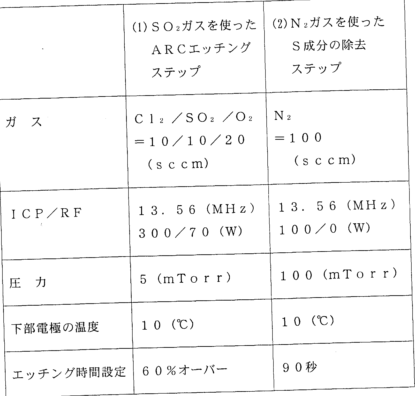
(第 6の実施形態) (Sixth embodiment)
第 6の実施形態は、 S成分を有するガスを含むエッチングガスを用いてドライ エッチングを行なった後に、 S成分を含まないガス例えば N 2 ガスよりなるブラ ズマの処理を施す場合において、 ポリシリコン膜 4 3等の下地膜の凹凸量や下地 膜の種類によって、 プラズマ処理の時間、 ガス圧力、 ガス流量、 処理温度及び高 周波電力の出力を制御するものである。 ドライエッチングを行なう装置について
は、 特に問題にならないが、 比較のために、 図 2に示した第 1のドライエツチン グ装置を用い、 被エッチング膜については図 4に示した構成のものとした。 第 6の実施形態に係る S〇2 ガスを用いる有機系反射防止膜 44に対するエツ チングプロセス条件は [表 1 5] に示す通りであり、 N2 ガスよりなるプラズマ のプラズマ処理は [表 1 6] に示す通りである。 The sixth embodiment is characterized in that, after performing dry etching using an etching gas containing a gas having an S component, and then performing a plasma treatment using a gas containing no S component, for example, N 2 gas, the polysilicon film The plasma processing time, gas pressure, gas flow rate, processing temperature, and output of high-frequency power are controlled by the amount of unevenness of the base film such as 43 and the type of the base film. Equipment for dry etching Although there is no particular problem, for comparison, the first dry etching apparatus shown in FIG. 2 was used, and the film to be etched was configured as shown in FIG. Etsu quenching process conditions for the organic antireflection film 44 using S_〇 2 gas according to the sixth embodiment is as shown in Table 1 5] The plasma treatment of the plasma composed of N2 gas [Table 1 6] As shown in FIG.
【表 1 5】 [Table 15]
エッチングプロセス条件 Etching process conditions
【表 1 6】 [Table 16]
プラズマ処理条件 Plasma processing conditions
図 4 (a) に示す有機系反射防止膜 44を、 図 4 (b) に示すように S02 ガ スを用いて 60 %相当のドライエッチングをした後、 ポリシリコン膜 43を N 2 ガスよりなるプラズマによりプラズマ処理する。 The organic antireflection film 44 shown in FIG. 4 (a), after 60% equivalent dry-etched using the S0 2 gas as shown in FIG. 4 (b), the polysilicon film 43 from the N 2 gas Plasma treatment is performed using the resulting plasma.
図 8は、 N2 ガスよりなるプラズマの処理時間及びポリシリコン膜 43のダレ ィンサイズを変'化させたときの、 グレインサイズとボリシリコン膜 43上のパー ティクル数との関係を示している。 パ一ティクル数は、 レ一ザ一光をポリシリコ ン膜 43上に照射したときの光学的な反射によってカウントしており、 個数 Z8 ィンチウェハで示している。 FIG. 8 shows the relationship between the grain size and the number of particles on the polysilicon film 43 when the processing time of the plasma made of N 2 gas and the drainage size of the polysilicon film 43 are changed. The number of particles is counted by optical reflection when one laser beam is irradiated onto the polysilicon film 43, and the number is indicated by a Z8 inch wafer.
図 8から分かるように、 ポリシリコン膜 43のグレインサイズを 0. 5 zmか ら 0. 05 mまで小さくするに伴って、 ポリシリコン膜 43上のパーティクル 数は減少している。 これは、 グレインサイズが大きいほどグレイン及びグレイン の界面の凹凸が大きく、 S系の残留物が多く残るためと考えられる。 また、 N2 ガスよりなるプラズマの処理時間を 30秒から 90秒に長くすることによって、 ポリシリコン膜 43上のパーティクル数を減少させることができる。 つまり、 ポ リシリコン膜 43のグレインサイズに応じて N2 ガスよりなるプラズマの処理時 間を増加することによって、 ポリシリコン膜 43及びレジストパターン 45の上 の S系の残留物を低減し、 これにより、 パーティクル数を減少させることができ る。 As can be seen from FIG. 8, as the grain size of the polysilicon film 43 is reduced from 0.5 zm to 0.05 m, the number of particles on the polysilicon film 43 decreases. This is presumably because the larger the grain size, the larger the irregularities of the grains and the interface between the grains and the more S-based residues remain. Further, by increasing the processing time of the plasma made of N 2 gas from 30 seconds to 90 seconds, the number of particles on the polysilicon film 43 can be reduced. That is, by increasing the processing time of the plasma composed of the N 2 gas in accordance with the grain size of the polysilicon film 43, the S-based residue on the polysilicon film 43 and the resist pattern 45 is reduced, thereby reducing The number of particles can be reduced.
図 9は、 プラズマ処理の N2 ガスのガス圧力及びポリシリコン膜の 33のダレ ィンサイズを変化させたときの、 グレインサイズとポリシリコン膜 43上のパー ティクル数との関係を示している。 パーティクル数は、 レーザー光をポリシリコ ン膜 43上に照射したときの光学的な反射によってカウントしており、 個数 Z8 ィンチウェハで示している。 FIG. 9 shows the relationship between the grain size and the number of particles on the polysilicon film 43 when the gas pressure of the N 2 gas in the plasma treatment and the drainage size of the polysilicon film 33 are changed. The number of particles is counted by optical reflection when laser light is irradiated onto the polysilicon film 43, and the number is indicated by a Z8 inch wafer.
図 9から分かるように、 ポリシリコン膜 43のグレインサイズを 0. か ら 0. 05 μπ まで小さくするに伴って、 ポリシリコン膜 43上のパーティクル 数は減少している。 また、 プラズマ処理の Ν2 ガスの圧力を 1 OmT o r rから 1 0 OmT o r rに高くすることによって、 ポリシリコン膜 43上のパーティク ル数は減少させることができる。 つまり、 ポリシリコン膜 43のグレインサイズ ひいてはポリシリコン膜 43表面の凹凸に応じてプラズマ処理の ガスのガス
圧力を高くすることによって、 ポリシリコン膜 4 3及びレジストパターン 4 5の 上の S系の残留物を低減し、 これにより、 パ一ティクル数を減少させることがで さる。 As can be seen from FIG. 9, as the grain size of the polysilicon film 43 is reduced from 0. to 0.05 μπ, the number of particles on the polysilicon film 43 decreases. The number of particles on the polysilicon film 43 can be reduced by increasing the pressure of the second gas in the plasma treatment from 10 OmTorr to 10 OmTorr. In other words, depending on the grain size of the polysilicon film 43 and, consequently, the roughness of the surface of the polysilicon film 43, By increasing the pressure, the S-based residue on the polysilicon film 43 and the resist pattern 45 is reduced, whereby the number of particles can be reduced.
図 1 0は、 プラズマ処理の N 2 ガスのガス流量及びボリシリコン膜 4 3のダレ ィンサイズを変'化させたときの、 グレインサイズとポリシリコン膜 4 3上のパ一 ティクル数との関係を示している。 パーティクル数は、 レーザー光をポリシリコ ン膜 4 3上に照射したときの光学的な反射によってカウントしており、 個数 Z 8 ィンチウェハで示している。 FIG. 10 shows the relationship between the grain size and the number of particles on the polysilicon film 43 when the gas flow rate of N 2 gas in the plasma treatment and the drainage size of the polysilicon film 43 are changed. Is shown. The number of particles is counted by optical reflection when laser light is irradiated onto the polysilicon film 43, and the number is indicated by a Z8 inch wafer.
図 1 0から分かるように、 ポリシリコン膜 4 3のグレインサイズを 0 . 5 j m から 0 . 0 5 mまで小さくするに伴って、 ポリシリコン膜 4 3上のパーテイク ル数は減少している。 また、 ガスよりなるプラズマ処理のガス流量を 2 0 s c c mから 8 0 s c c mまで多くすることによって、 ポリシリコン膜 4 3上のパ —ティクル数は減少させることができる。 つまり、 ポリシリコン膜 4 3のグレイ ンサイズひいてはポリシリコン膜 4 3表面の凹凸に応じてプラズマ処理の N 2 ガ スのガス流量を多くすることにより、 ポリシリコン膜 4 3及びレジストパターン 4 5の上の S系の残留物を低減し、 これにより、 パーティクル数を減少させるこ とができる。 As can be seen from FIG. 10, as the grain size of the polysilicon film 43 decreases from 0.5 jm to 0.05 m, the number of particles on the polysilicon film 43 decreases. Also, by increasing the gas flow rate of the plasma processing of gas from 20 sccm to 80 sccm, the number of particles on the polysilicon film 43 can be reduced. In other words, by increasing the gas flow rate of the N 2 gas in the plasma processing according to the grain size of the polysilicon film 43 and, consequently, the unevenness of the surface of the polysilicon film 43, the upper surface of the polysilicon film 43 and the resist pattern 45 is increased. Therefore, it is possible to reduce the number of particles in the S system, thereby reducing the number of particles.
図 1 1は、 N 2 ガスよりなるプラズマ処理におけるシリコンウェハ 4 1の温度 及びポリシリコン膜 4 3のグレインサイズを変化させたときの、 グレインサイズ とポリシリコン膜 4 3上のパーティクル数との関係を示している。 パーティクル 数は、 レーザー光をポリシリコン膜 4 3上に照射したときの光学的な反射によつ てカウントしており、 個数 / 8インチウェハで示している。 Fig. 11 shows the relationship between the grain size and the number of particles on the polysilicon film 43 when the temperature of the silicon wafer 41 and the grain size of the polysilicon film 43 are changed in the plasma treatment using N 2 gas. Is shown. The number of particles is counted by optical reflection when a laser beam is irradiated onto the polysilicon film 43, and is shown as a number of / 8 inch wafers.
図 1 1から分かるように、 ポリシリコン膜 4 3のグレインサイズを 0 . 5 ^ m から 0 . 0 5 mまで小さくするに伴って、 ポリシリコン膜 4 3上のパーテイク ル数は減少している。 また、 N 2 ガスよりなるプラズマ処理におけるシリコンゥ ェハ 4 1の温度を一 1 0 °Cから 5 0 °Cに高くすることによって、 ポリシリコン膜 4 3上のパーティクル数を減少させることができる。 つまり、 ポリシリコン膜 4 3のグレインサイズひいてはポリシリコン膜 4 3表面の凹凸に応じて N 2 ガスよ りなるプラズマ処理におけるシリコンウェハ 4 1の温度を高くすることによって
、 ポリシリコン膜 43及びレジストパターン 45の上の S系の残留物を低減し、 これにより、 パーティクル数を減少させることができる。 As can be seen from FIG. 11, the number of particles on the polysilicon film 43 decreases as the grain size of the polysilicon film 43 decreases from 0.5 ^ m to 0.05 m. . Further, by increasing the temperature of silicon wafer 41 in plasma processing using N 2 gas from 110 ° C. to 50 ° C., the number of particles on polysilicon film 43 can be reduced. In other words, by increasing the temperature of the silicon wafer 41 in the plasma processing using N 2 gas in accordance with the grain size of the polysilicon film 43 and thus the roughness of the surface of the polysilicon film 43. The S-based residue on the polysilicon film 43 and the resist pattern 45 can be reduced, thereby reducing the number of particles.
図 1 2は、 N2 ガスよりなるプラズマ処理における LEPパワー及びポリシリ コン膜 43のグレインサイズを変化させたときの、 グレインサイズとポリシリコ ン膜 43上のパーティクル数との関係を示している。 パーティクル数は、 レーザ 一光をポリシリコン膜 43上に照射したときの光学的な反射によってカウントし ており、 個数 8インチウェハで示している。 FIG. 12 shows the relationship between the grain size and the number of particles on the polysilicon film 43 when the LEP power and the grain size of the polysilicon film 43 are changed in the plasma treatment using N 2 gas. The number of particles is counted by optical reflection when one laser beam is irradiated onto the polysilicon film 43, and the number is shown by an 8-inch wafer.
図 1 2から分かるように、 ポリシリコン膜 43のグレインサイズを 0. 5 m から 0. 05 mまで小さくするに伴って、 ポリシリコン膜 43上のパーテイク ル数は減少している。 また、 N2 ガスよりなるプラズマ処理における LEPパヮ —を 50Wから 1 50Wまで大きくすることによって、 ポリシリコン膜 43上の パ一ティクル数を減少させることができる。 つまり、 ポリシリコン膜 43のダレ インサイズひいてはポリシリコン膜 43表面の凹凸に応じて、 N2 ガスよりなる プラズマ処理における LEPパワーを大きくすることにより、 ポリシリコン膜 4 3及びレジストパ夕一ン 45の上の S系の残留物を低減し、 これにより、 パ一テ ィクル数を減少させることができる。 As can be seen from FIG. 12, as the grain size of the polysilicon film 43 is reduced from 0.5 m to 0.05 m, the number of particles on the polysilicon film 43 decreases. Also, by increasing the LEP power in the plasma treatment using N 2 gas from 50 W to 150 W, the number of particles on the polysilicon film 43 can be reduced. In other words, by increasing the LEP power in the plasma treatment using N 2 gas in accordance with the drain size of the polysilicon film 43 and consequently the unevenness of the surface of the polysilicon film 43, the polysilicon film 43 and the resist pattern 45 are reduced. The residue of the above-mentioned S system is reduced, whereby the number of particles can be reduced.
図 1 3は、 N2 ガスよりなるプラズマ処理における R Fパワー及びポリシリコ ン膜 43のグレインサイズを変化させたときの、 グレインサイズとポリシリコン 膜 43上のパ一ティクル数との関係を示している。 パーティクル数は、 レーザ一 光をポリシリコン膜 43上に照射したときの光学的な反射によってカウントして おり、 個数 / 8インチウェハで示している。 FIG. 13 shows the relationship between the grain size and the number of particles on the polysilicon film 43 when the RF power and the grain size of the polysilicon film 43 are changed in the plasma processing using N 2 gas. . The number of particles is counted by optical reflection when a laser beam is irradiated onto the polysilicon film 43, and is shown by the number of / 8 inch wafers.
図 1 3から分かるように、 ポリシリコン膜 43のグレインサイズを 0. 5〃m から 0. 05 mまで小さくするに伴って、 ポリシリコン膜 43上のパーテイク ル数は減少している。 また、 N2 ガスよりなるプラズマ処理における RFパワー を 50Wから 1 50Wまで大きくすることによって、 ボリシリコン膜 43上のパ —ティクル数を減少させることができる。 つまり、 ボリシリコン膜 43のグレイ ンサイズひいてはポリシリコン膜 43表面の凹凸に応じて N 2 ガスよりなるブラ ズマ処理における RFパワーを大きくすることにより、 ポリシリコン膜 43及び レジストパターン 45の上の S系の残留物を低減し、 これにより、 パーティクル
数を減少させることができる。 As can be seen from FIG. 13, as the grain size of the polysilicon film 43 is reduced from 0.5 μm to 0.05 m, the number of particles on the polysilicon film 43 decreases. Also, by increasing the RF power in the plasma processing using N 2 gas from 50 W to 150 W, the number of particles on the polysilicon film 43 can be reduced. In other words, by increasing the RF power in the plasma processing of N 2 gas in accordance with the grain size of the polysilicon film 43 and, consequently, the unevenness of the surface of the polysilicon film 43, the S-system on the polysilicon film 43 and the resist pattern 45 is increased. Reduce the residue of the particles The number can be reduced.
図 1 4は、 下地膜の種類及び N 2 ガスよりなるプラズマの処理時間を変化させ たときの、 処理時間とポリシリコン膜 4 3上のパーティクル数との関係を示して いる。 パーティクル数は、 レーザー光をポリシリコン膜 4 3上に照射したときの 光学的な反射に'よってカウントしており、 個数 Z 8インチウェハで示している。 図 1 4から分かるように、 下地膜の種類が、 アモルファスシリコン膜、 ポリシ リコン膜、 W S i膜又は T E O S膜と変わることにより、 N 2 ガスよりなるブラ ズマ処理後のパーティクル数は変化している。 また、 N 2 ガスよりなるプラズマ 処理時間を 0秒から 9 0秒に長くすることによって、 下地膜上のパ一ティクル数 を減少させることができる。 つまり、 下地膜の変化に応じて N 2 ガスよりなるプ ラズマ処理時間を変化させることにより、 パーティクルを減少させることができ る。 FIG. 14 shows the relationship between the processing time and the number of particles on the polysilicon film 43 when the type of the base film and the processing time of the plasma composed of N 2 gas are changed. The number of particles is counted based on optical reflection when laser light is irradiated onto the polysilicon film 43, and the number of particles is indicated by an 8-inch wafer. As it can be seen from FIGS. 1-4, the type of underlying film, an amorphous silicon film, policy silicon film, by changing the WS i film or a TEOS film, the number of particles after bra Zuma process consisting N 2 gas has changed . In addition, the number of particles on the base film can be reduced by increasing the plasma processing time of N 2 gas from 0 seconds to 90 seconds. In other words, particles can be reduced by changing the plasma processing time of N 2 gas according to the change of the base film.
尚、 以上においては、 下地膜の変化に対応する N 2 ガスよりなるプラズマ処理 の変化の効果をプラズマ処理時間を例にとつて説明したが、 プラズマ処理におけ る、 ガス圧力、 ガス流量、 L E Pパワー、 R Fパワー又はシリコンウェハ 4 1の 温度等を変化させても、 同様の効果が得られることは言うまでもない。 In the above description, the effect of the change in the plasma processing made of N 2 gas corresponding to the change in the base film has been described using the plasma processing time as an example.However, in the plasma processing, the gas pressure, gas flow rate, LEP It goes without saying that the same effect can be obtained by changing the power, the RF power, the temperature of the silicon wafer 41 or the like.
(第 7の実施形態) (Seventh embodiment)
第 7の実施形態は、 有機系反射防止膜に対して S〇2 系のエッチングガスを用 いてドライエッチングを行なった後、 シリコンウェハ 4 1を加熱することにより 、 ポリシリコン膜 4 3、 レジストパターン 4 5及び有機系反射防止膜 4 4の上に 存在する S成分を有する残留物を気化して除去するものである。 In the seventh embodiment, the organic antireflection film is subjected to dry etching using an S〇2-based etching gas, and then the silicon film 41 is heated to form the polysilicon film 43 and the resist pattern. The residue containing the S component existing on the antireflection film 44 and the organic antireflection film 44 is vaporized and removed.
ドライエッチングを行なう装置については、'特に問題にならないが、 比較のた めに、 図 2に示した第 1のドライエッチング装置を用い、 被エッチング膜につい ては図 4に示した構成のものとした。 There is no particular problem with the equipment that performs dry etching, but for comparison, the first dry etching equipment shown in Fig. 2 was used for comparison, and the film to be etched was the same as the one shown in Fig. 4. did.
第 7の実施形態に係る S〇2 ガスを用いる有機系反射防止膜 4 4に対するエツ チングのエッチングプロセス条件は、 [表 1 7 ] に示す通りである。
【表 1 7】 Etching process conditions Etsu quenching an organic antireflection film 4 4 using S_〇 2 gas according to the seventh embodiment is as shown in Table 1 7]. [Table 17]
エッチングプロセス条件 Etching process conditions
有機系反射防止膜 4 4に対して S 0 2 ガスを用いてドライエッチングした後、 シリコンウェハ 4 1をホットプレート上に設置して 1分間加熱する。 After dry-etched using the S 0 2 gas to the organic anti-reflection film 4 4, heated for 1 minute by installing a silicon wafer 4 1 on the hot plate.
図 1 5は、 ホッ トプレートの加熱温度を変化させたときの、 加熱温度とポリシ リコン膜 4 3上のパーティクル数との関係を示している。 パ一ティクル数は、 レ 一ザ一光をポリシリコン膜 4 3上に照射したときの光学的な反射によってカウン 卜しており、 個数 / 8インチウェハで示している。 FIG. 15 shows the relationship between the heating temperature and the number of particles on the polysilicon film 43 when the heating temperature of the hot plate is changed. The number of particles is counted by optical reflection when a laser beam is irradiated onto the polysilicon film 43, and is expressed by the number of wafers / 8 inch.
図 1 5から分かるように、 加熱温度を 3 0 °Cから上昇させるに伴って、 ポリシ リコン膜 4 3上のパーティクル数は減少し、 特に加熱温度が 7 0 °C以上になると パーティクル数は大きく減少する。 これに対じて、 加熱温度が 1 2 0 °C以上にな ると、 レジストパターン 4 5の形状が変形するので、 加熱温度は 7 0〜 1 2 0 °C の範囲が好ましい。 また、 加熱温度が 1 0 0 °C以上になると、 パーティクル数は 1 0個以下で殆ど変化していないので、 加熱温度としては 1 0 0 °C程度が特に好 ましい。 As can be seen from Fig. 15, as the heating temperature is increased from 30 ° C, the number of particles on the polysilicon film 43 decreases, especially when the heating temperature is 70 ° C or higher. Decrease. On the other hand, if the heating temperature exceeds 120 ° C., the shape of the resist pattern 45 is deformed. Therefore, the heating temperature is preferably in the range of 70 to 120 ° C. When the heating temperature is 100 ° C. or higher, the number of particles is less than 10 and hardly changes. Therefore, the heating temperature is particularly preferably about 100 ° C.
図 1 6は、 シリコンウェハ 4 1をホットプレートにより 1 0 0 °Cに加熱したと きの、 加熱時間とポリシリコン膜 4 3上のパーティクル数との関係を示している 。 パーティクル数は、 レーザー光をポリシリコン膜 4 3上に照射したときの光学
的な反射によってカウントしており、 個数 Z 8ィンチウェハで示している。 FIG. 16 shows the relationship between the heating time and the number of particles on the polysilicon film 43 when the silicon wafer 41 is heated to 100 ° C. by a hot plate. The number of particles depends on the optics when laser light is irradiated onto the polysilicon film 43. The number is represented by a typical reflection, and the number is indicated by a Z8 inch wafer.
図 1 6から分かるように、 加熱時間を 0秒から 6 0秒まで増加させるに伴って As can be seen from Fig. 16, as the heating time increases from 0 seconds to 60 seconds,
、 ポリシリコン膜 4 3上のパーティクル数は減少しているが、 加熱時間が 6 0秒 以上になると、 パーティクル数は 1 0個以下で殆ど変化しない。 Although the number of particles on the polysilicon film 43 is decreasing, when the heating time is 60 seconds or more, the number of particles is less than 10 and hardly changes.
また、 図 1 7は、 加熱温度と T D S (Therma l Des ola t i on mass Spec t roscopy Fig. 17 shows the heating temperature and TDS (Thermal Desolati on mass Spectroscopy).
) 法による S 0 2 成分の検出強度との関係、 つまり加熱温度と S成分の脱離との 関係を示している。 ) S 0 2 relationship between detected intensity of the components, i.e. shows a desorption Metropolitan relationship of the heating temperature and the S component due method.
図 1 7から分かるように、 加熱温度が 0 °Cから 3 0 0 °Cまでの間では、 多少の ばらつきはあるが、 加熱温度を上げるに伴って S〇2 の放出量が増加している。 以上の結果から、 有機系反射防止膜 4 4を S〇 ガスを用いてドライエツチン グした後、 シリコンウェハ 4 1をホットプレート上で加熱することにより、 ポリ シリコン膜 4 3及びレジストパターン 4 5上の S系の残留物が気化して除去され るので、 パーティクル数を減少することができる。 As can be seen from FIG. 1 7, between the heating temperature is from 0 ° C to 3 0 0 ° C, although there are some variations, the amount of emitted S_〇 2 with the raising the heating temperature is increased . From the above results, the organic anti-reflection film 44 was dry-etched using S〇 gas, and then the silicon wafer 41 was heated on a hot plate, so that the polysilicon film 43 and the resist pattern 45 were not etched. Since the S-based residue is vaporized and removed, the number of particles can be reduced.
(第 8の実施形態) (Eighth embodiment)
第 8の実施形態は、 有機系反射防止膜に対して S〇 系のエッチングガスを用 いてドライエッチングを行なった後、 シリコンウェハ 4 1を温水で洗浄すること により、 ポリシリコン膜 4 3、 レジストパターン 4 5及び有機系反射防止膜 4 4 上に存在する S成分を有する残留物を除去するものである。 In the eighth embodiment, the organic antireflection film is dry-etched using an S〇-based etching gas, and then the silicon wafer 41 is washed with warm water to form the polysilicon film 43 and the resist. This removes the residue having the S component existing on the pattern 45 and the organic antireflection film 44.
ドライエッチングを行なう装置については、 特に問題にならないが、 比較のた めに、 図 2に示した第 1のドライエッチング装置を用い、 被エッチング膜につい ては図 4に示した構成のものとした。 There is no particular problem with the equipment used for dry etching, but for comparison, the first dry etching equipment shown in Fig. 2 was used, and the film to be etched was configured as shown in Fig. 4. .
第 8の実施形態に係る S〇 ガスを用いる有機系反射防止膜 4 4に対するエツ チングのエッチングプロセス条件は、 [表 1 8 ] に示す通りである。
The etching process conditions for etching the organic antireflection film 44 using the sulfuric acid gas according to the eighth embodiment are as shown in [Table 18].
【表 1 8】 [Table 18]
エッチングプロセス条件 Etching process conditions
有機系反射防止膜 4 4に対して S 0 2 ガスを用いてドライエッチングした後、 シリコンウェハ 4 1を水洗槽にて 9 0秒間洗浄する。 After dry-etched using the S 0 2 gas to the organic anti-reflection film 4 4, washed 9 0 seconds silicon wafer 4 1 at washing tank.
図 1 8は、 水洗温度を変化させたときの、 水洗温度とポリシリコン膜 4 3上の パーティクル数との関係を示している。 パーティクル数は、 レーザ一光をポリシ リコン膜 4 3上に照射したときの光学的な反射によってカウントしており、 個数 Z 8インチウェハで示している。 FIG. 18 shows the relationship between the washing temperature and the number of particles on the polysilicon film 43 when the washing temperature is changed. The number of particles is counted by optical reflection when one laser beam is irradiated onto the polysilicon film 43, and the number is indicated by an 8-inch wafer.
図 1 8から分かるように、 水洗温度を 2 0 °Cから 1 0 0 °Cまで上昇させるに伴 つて、 ポリシリコン膜 4 3上のパーティクル数は減少している。 しかしながら、 水は 1 0 0 °Cで沸縢するので、 9 0 °C以下の水洗温度で洗浄しなければならない 図 1 9は、 シリコンウェハ 4 1を 7 0 °Cの水洗漕で洗浄したときの、 洗浄時間 とポリシリコン膜 4 3上のパーティクル数との関係を示している。 パ一ティクル 数は、 レーザー光をポリシリコン膜 4 3上に照射したときの光学的な反射によつ てカウントしており、 個数 Z 8インチウェハで示している。 As can be seen from FIG. 18, the number of particles on the polysilicon film 43 decreases as the rinsing temperature is increased from 20 ° C. to 100 ° C. However, water boil at 100 ° C, so it must be washed at a washing temperature of 90 ° C or less.Figure 19 shows the results when silicon wafer 41 was washed in a 70 ° C washing tank. The relationship between the cleaning time and the number of particles on the polysilicon film 43 is shown. The number of particles is counted by optical reflection when a laser beam is irradiated onto the polysilicon film 43, and the number of particles is indicated by an 8-inch wafer.
図 1 9から分かるように、 洗浄時間を 0秒から 1 2 0秒まで増加させるに伴つ て、 ポリシリコン膜 4 3上のパーティクル数は減少している。 しかしながら、 洗
浄時間が 120秒以上になると、 パーティクル数は 1 0個以下で殆ど変化しない 以上の結果から、 有機系反射防止膜 44を S 02 ガスを用いてドライエツチン グした後、 シリコンウェハ 41を温水で洗浄することにより、 ポリシリコン膜 4 3及びレジス卜パターン 45上の S系の残留物が気化して除去されるので、 パー ティクル数を減少することができる。 As can be seen from FIG. 19, as the cleaning time increases from 0 seconds to 120 seconds, the number of particles on the polysilicon film 43 decreases. However, washing When purification time is 120 seconds or more, the number of particles from most or unchanged results with 1 0 or less, the organic antireflection film 44 after Doraietsuchin grayed with S 0 2 gas, the silicon wafer 41 with warm water By cleaning, the S-based residue on the polysilicon film 43 and the resist pattern 45 is vaporized and removed, so that the number of particles can be reduced.
(第 9の実施形態) (Ninth embodiment)
第 9の実施形態は、 有機系反射防止膜に対して S〇 系のエッチングガスを用 いてドライエッチングを行なった後、 シリコンウェハ 4 1上に残存している酸性 である硫酸系残留物をアル力リ性溶液であるリソグラフィ一の現像液で中和して 洗浄することにより、 ポリシリコン膜 43、 レジストパターン 45及び有機系反 射防止膜 44上に存在する S成分を有する残留物を除去するものである。 In the ninth embodiment, after an organic antireflection film is dry-etched using an S 系 -based etching gas, acidic sulfuric acid-based residues remaining on the silicon wafer 41 are removed. Neutralization and cleaning with a lithographic developing solution, which is a strong solution, removes residues having the S component existing on the polysilicon film 43, the resist pattern 45, and the organic antireflection film 44. Things.
ドライエッチングを行なう装置については、 特に問題にならないが、 比較のた めに、 図 2に示した第 1のドライエッチング装置を用い、 被エッチング膜につい ては図 4に示した構成のものとした。 There is no particular problem with the equipment used for dry etching, but for comparison, the first dry etching equipment shown in Fig. 2 was used, and the film to be etched was configured as shown in Fig. 4. .
第 9の実施形態に係る S〇2 ガスを用いる有機系反射防止膜 44に対するエツ チングのエッチングプロセス条件は、 [表 1 9] に示す通りである。 Etching process conditions Etsu quenching an organic anti-reflective film 44 using S_〇 2 gas according to a ninth embodiment is shown in Table 1-9.
【表 1 9】 [Table 19]
エッチングプロセス条件 so2 / O 2 32/8 (s c cm) Etching process conditions so 2 / O 2 32/8 (sc cm)
L E P/R F 54. 24/ 1 3. 56 (MH z ) L E P / R F 54. 24/1 3.56 (MHz)
3 X 1 00 /70 (W) 圧 力 5 (mT 0 r r j 下部電極の温度 20 (°C)
有機系反射防止膜 44に対して S〇 ガスを用いてドライエッチングすると、 シリコンウェハ 41の上には硫酸系の残留物が残存している。 この硫酸系の残留 物をアルカリ性の溶液である現像液により中和して除去する。 その後、 シリコン ウェハ 4 1及び有機系反射防止膜 44を水で洗浄して、 残留する現像液を除去す る。 現像液は一般的に半導体製造工程のリソグラフィ一にて用いられているもの を用いた。 現像液は、 TMH (Tri-Methyl anmonium Hydrooxide) を主成分とし ており、 アル力リ金属を含まないので金属汚染は発生しない。 3 X 100/70 (W) Pressure 5 (mT 0 rrj Lower electrode temperature 20 (° C) When the organic antireflection film 44 is dry-etched using S〇 gas, a sulfuric acid-based residue remains on the silicon wafer 41. The sulfuric acid-based residue is neutralized and removed by a developer which is an alkaline solution. Thereafter, the silicon wafer 41 and the organic antireflection film 44 are washed with water to remove the remaining developer. The developer used was one generally used in lithography in the semiconductor manufacturing process. The developer contains TMH (Tri-Methyl anmonium Hydrooxide) as a main component, and does not contain metal salts, so that metal contamination does not occur.
図 20は、 硫酸系の残留物を 22°Cの現像液で中和したときの、 中和時間とポ リシリコン膜 43上のパーティクル数との関係を示している。 パーティクル数は 、 レーザ一光をポリシリコン膜 43上に照射したときの光学的な反射によって力 ゥン卜しており、 個数 Z 8インチウェハで示している。 図 20から分かるように 、 現像時間を 0秒から 1 20秒まで増加するに伴つて 、 ポリシリコン膜 43上の パーティクル数は減少している。 しかしながら、 現像時間が 1 20秒以上では、 パーティクル数は 1 0個以下で殆ど変化しない。 FIG. 20 shows the relationship between the neutralization time and the number of particles on the polysilicon film 43 when the sulfuric acid-based residue is neutralized with a developer at 22 ° C. The number of particles is counted by optical reflection when one laser beam is irradiated onto the polysilicon film 43, and the number of particles is indicated by an 8-inch wafer. As can be seen from FIG. 20, as the development time increases from 0 seconds to 120 seconds, the number of particles on the polysilicon film 43 decreases. However, when the developing time is longer than 120 seconds, the number of particles is less than 10 and hardly changes.
以上の結果かち、 有機系反射防止膜 44を S02 ガスを用いてドライエツチン グした後、 シリコンウェハ 4 1上の酸性の残留物をアルカリ性の現像液で中和し 、 その後、 現像液を水で洗浄することにより、 ボリシリコン膜 43及びレジス卜 パターン 45上の S系の残留物が除去されるので、 パーティクル数を減少させる ことができる。 Achieved As a result, the organic antireflection film 44 and Doraietsuchin grayed with S0 2 gas, a residue of acid on the silicon wafer 4 1 neutralized with an alkaline developing solution, then, the developer with water By cleaning, the S-based residue on the polysilicon film 43 and the resist pattern 45 is removed, so that the number of particles can be reduced.
尚、 第 5〜第 9の実施形態においては、 有機系反射防止膜 44の下地膜として ポリシリコン膜 43を用いたが、 S成分を有するガスを含むエッチングガスを用 いてドライエッチングを行なった後に、 残留する S成分を除去する後処理は、 下 地膜が TEO S等の酸化膜、 窒化膜、 タングステンシリサイ ド膜、 メタル合金膜 又は強誘電体膜等の場合でも、 同様の効果が得られることは言うまでもない。 また、 第 1〜第 9の実施形態においては、 図 2に示す LEP (Lissajous Elec tron Plasma) 方式の第 1のドライエッチング装置を用いたが、 これに代えて、 例えば、 R I E (Reactive Ion Etching ) 、 ECR (Electron Cyclotron Re sonance) 、 I CP (Inductive Coupled Plasma) 又は TCP (Trans former Cou pled Plasma) 方式等のプラズマ源を有するドライエッチング装置を用いても、 同
搽の効果が得られることは言うまでもない。 In the fifth to ninth embodiments, the polysilicon film 43 is used as a base film of the organic anti-reflection film 44. However, after performing dry etching using an etching gas containing a gas having an S component, The same effect can be obtained even if the underlying film is an oxide film such as TEOS, nitride film, tungsten silicide film, metal alloy film, ferroelectric film, etc. Needless to say. Further, in the first to ninth embodiments, the first dry etching apparatus of the LEP (Lissajous Electron Plasma) type shown in FIG. 2 was used, but instead, for example, RIE (Reactive Ion Etching) , ECR (Electron Cyclotron Resonance), ICP (Inductive Coupled Plasma) or TCP (Transformer Coupled Plasma) Needless to say, the effect of 搽 can be obtained.
(第 1 0の実施形態) (10th embodiment)
第 1 0の実施形態は、 前記の第 2の知見に基づいてなされたものであって、 具 体的には、 シリコン含有の有機系反射防止膜 4 4に対して、 ハロゲン系である C The tenth embodiment is based on the second finding described above. Specifically, the silicon-containing organic anti-reflection film 44 has a halogen-based C property.
1 2 Z〇2 系のエッチングガスを用いてドライエッチングを行なうものである。 尚、 第 1 0の実施形態で使用した有機系反射防止膜の材料 (商品名 : C D 9 ; ァ メリ力、 ブリューヮサイエンス社製) には、 分析の結果 1 0 p p m程度のシリコ ンが混入されていた。 Dry etching is performed using a 1 2 Z〇2-based etching gas. As a result of the analysis, about 10 ppm of silicon was mixed in the material of the organic anti-reflection film used in the tenth embodiment (trade name: CD9; Amerikari, manufactured by Brewery Science Co., Ltd.). It had been.
ドライエッチングを行なう装置については、 特に問題にならないが、 比較のた め、 図 3に示した第 2のドライエッチング装置を用い、 被エッチング膜について は図 4に示した構成のものとした。 Although there is no particular problem with the apparatus for performing the dry etching, for comparison, the second dry etching apparatus shown in FIG. 3 was used, and the film to be etched was configured as shown in FIG.
第 1 0の実施形態に係るエッチングのエッチングプロセス条件は、 [表 2 0 ] に示す通りである。 The etching process conditions for the etching according to the tenth embodiment are as shown in [Table 20].
【表 2 0】 [Table 20]
エッチングプロセス条件 Etching process conditions
また、 エッチング特性結果は [表 2 1 ] に示す通りであって、 有機系反射防止 膜 4 4に多少の寸法変動は存在するが、 垂直形状が得られると共に、 N 2 O 2 系のガスを用いる従来のエッチングにおいて発生していた異物状残渣は全く発生 しなかった。
【表 2 1】 The results of the etching characteristics are shown in [Table 21]. The organic anti-reflection coating 44 has some dimensional fluctuations, but a vertical shape is obtained and N 2 O 2 gas is removed. No foreign residue generated in the conventional etching used was generated at all. [Table 21]
エッチング特性結果 Etching characteristics results
このように、 異物状残渣が発生しなかった理由は、 シリコン含有の有機系反射 防止膜 44中のシリコンが、 C 12 /02 系のエッチングガスに含まれる C 1 ラジカルによりエッチングされ、 未反応のシリコン成分が存在しないためである と考えられる。 The reason for the foreign matter-like residue is not generated, the silicon in the organic antireflection film 44 of the silicon-containing is etched by C 1 radicals contained in C 1 2/02-based etching gas, unreacted It is considered that this is because no silicon component exists.
(第 1 1の実施形態) (Eleventh Embodiment)
第 1 1の実施形態も、 前記の第 2の知見に基づいてなされたものであって、 具 体的には、 シリコン含有の有機系反射防止膜 4· 4に対して、 C l 2 / O 2 ガス系 に S 02 ガスが添加されてなるエッチングガスを用いてドライエッチングを行な うものである。 尚、 第 1 1の実施形態においても、 第 10の実施形態と同様、 有 機系反射防止膜の材料 (商品名 : CD 9 ; アメリカ、 ブリューヮサイエンス社製 ) を用いた。 また、 第 1 0の実施形態と同様、 図 3に示した第 2のドライエッチ ング装置を用い、 被エッチング膜については図 4に示した構成のものとした。 第 1 1の実施形態に係るエッチングのエッチングプロセス条件は、 [表 22] に示す通りである。 また、 エッチング特性結果は [表 23] に示す通りであって
、 垂直形状が得られると共に寸法変動も小さかった。 また、 第 1 0の実施形態と 同様、 異物状残渣は全く発生しなかった。 The first embodiment is also based on the above-mentioned second finding, and specifically, Cl 2 / O 2 is applied to the silicon-containing organic antireflection film 4. 2 gas system is the row of Umono dry etching using the S 0 2 etching gas gas is being added. In the eleventh embodiment, as in the tenth embodiment, a material for an organic anti-reflection film (trade name: CD9; manufactured by Brewery Science Co., USA) was used. Further, similarly to the tenth embodiment, the second dry etching apparatus shown in FIG. 3 was used, and the film to be etched was configured as shown in FIG. The etching process conditions for the etching according to the eleventh embodiment are as shown in [Table 22]. The etching characteristics are shown in [Table 23]. The vertical shape was obtained and the dimensional variation was small. Also, as in the tenth embodiment, no foreign residue was generated.
【表 22】 [Table 22]
エッチングプロセス条件 Etching process conditions
【表 23】 [Table 23]
エッチング特性結果 Etching characteristics results
A R Cエッチレート 1 500 (A/m i n) 均一性 ±4. 0 ( ) 寸法変動 0. 00 zm (o p e n) A R C etch rate 1 500 (A / min) Uniformity ± 4.0 () Dimensional variation 0.000 zm (open)
― 0. Ο Ι ΠΊ (d e n s e) ポリシリコン膜との CO ― 0. Ο Ι ΠΊ (d e n se) CO with polysilicon film
選択比 異物状残渣 なし
第 1 0の実施形態においては、 [表 2 1 ] に示すように、 エッチング後の有機 系反射防止膜 4 4の寸法がレジストパターン 4 5の寸法に比べて若干小さくなる 多少の寸法変動が存在したが、 第 1 1の実施形態においては寸法変動は小さかつ た。 エッチング後の有機系反射防止膜 4 4の寸法がレジストパターン 4 5の寸法 よりも小さくな'ると、 レジストパターン 4 5及び有機系反射防止膜 4 4をマスク としてポリシリコン膜 4 3に対してエッチングを行なうと、 得られるポリシリコ ン膜 4 3のパターン寸法が変動してしまうという問題が発生するが、 第 1 1の実 施形態によると、 得られるポリシリコン膜 4 3のパターン寸法は変動しない。 第 1 1の実施形態において、 異物状残渣物が発生しなかった理由は、 シリコン 含有の有機系反射防止膜 4 4中のシリコンが、 C l 2 / O z 2 系のエツ チングガスに含まれる C 1 ラジカルによりエッチングされ、 未反応のシリコン成 分が存在しないためであると考えられる。 Selectivity No foreign residue In the tenth embodiment, as shown in [Table 21], the dimensions of the organic antireflection film 44 after etching are slightly smaller than the dimensions of the resist pattern 45. However, the dimensional variation was small in the eleventh embodiment. When the dimension of the organic anti-reflection film 44 after etching becomes smaller than the dimension of the resist pattern 45, the resist pattern 45 and the organic anti-reflection film 44 are used as a mask to form a polysilicon film 43. The etching causes a problem that the pattern size of the obtained polysilicon film 43 changes, but according to the first embodiment, the pattern size of the obtained polysilicon film 43 does not change. . In the first embodiment, the reason why the foreign matter-like residue was not generated is that the silicon in the silicon-containing organic antireflection film 44 contained C 2 / Oz 2 -based etching gas. This is probably due to the fact that there was no unreacted silicon component that was etched by one radical.
また、 有機系反射防止膜 4 4の寸法変動が小さくなる理由は、 レジストパター ン 4 5及び有機系反射防止膜 4 4の主成分である Cとエツチャントである Sとが C S という形でガス化し難くなり、 C— S結合を持ったポリマー状の側壁保護 膜がレジストパターン 4 5や有機系反射防止膜 4 4の側壁に付着し易くなるので 、 有機系反射防止膜 4 4の寸法の細りが抑制されるためであると考えられる。 (第 1 2の実施形態) The reason that the dimensional variation of the organic anti-reflection film 44 is reduced is that C, which is the main component of the resist pattern 45 and the organic anti-reflection film 44, and S, which is an etchant, are gasified in the form of CS. It becomes difficult to adhere to the resist pattern 45 and the side wall of the organic anti-reflection film 44 because the polymer-type side wall protection film having a C—S bond is easily attached to the organic anti-reflection film 44. It is considered that this is because it is suppressed. (First and second embodiments)
第 1 2の実施形態は、 シリコン含有の有機系反射防止膜に対して、 C l Z S O 2 / O 2 ガスよりなるエッチングガスを用いてドライエッチングステップを行 なった後、 S成分を含まない不活性ガスである N 2 ガスを用いてプラズマ処理を 行なうものである。 - 尚、 第 1 2の実施形態においても、 第 1 0の実施形態と同様、 有機系反射防止 膜の材料 (商品名 : C D 9 ; アメリカ、 ブリューヮサイエンス社製) を用いた。 また、 第 1 0の実施形態と同様、 図 3に示した第 2のドライエッチング装置を 用い、 被エッチング膜については図 4に示した構成のものとした。 In the first embodiment, a silicon-containing organic antireflection film is subjected to a dry etching step using an etching gas composed of ClZSO2 / O2 gas. and performs plasma processing using the N 2 gas is inert gas. -In the 12th embodiment, as in the 10th embodiment, the material of the organic antireflection film (trade name: CD9; manufactured by Brew Science Inc., USA) was used. Further, as in the tenth embodiment, the second dry etching apparatus shown in FIG. 3 was used, and the film to be etched had the structure shown in FIG.
第 1 2の実施形態に係るエッチングプロセス条件及びプラズマ処理条件は、 [ 表 2 4 ] に示す通りであって、 イオンクロマトグラフィー法により Sの定量分析 を行なった結果は、 [表 2 5 ] に示す通りである。
【表 24】 The etching process conditions and plasma processing conditions according to the first embodiment are as shown in [Table 24]. The results of quantitative analysis of S by ion chromatography are shown in [Table 25]. As shown. [Table 24]
エッチングプロセス条件 Etching process conditions
【表 25】 ステップの イオンクロマ卜グラフィ法 組合せ による Sの定量 [Table 25] Quantitative determination of S by combination of step ion chromatography
(1) のみ 1 60 8ィンチウェハ (1) only 1 60 8 inch wafer
(1)+ (2) 30 gZ8ィンチウェハ
[表 25] に示すように、 (1) のステップのみを行なった場合、 すなわち、 シ リコン含有の有機系反射防止膜 44に対して C 12 /S 02 / 2 ガスよりなる エッチングガスを用いるドライエッチングのみを行なった場合には、 イオンクロ マトグラフィ一法による Sの定量分析の結果は、 1 60 /X g / 8インチウェハで あった。 これに対して、 (1) 及び(2) のステップを行なった場合、 すなわち、 シ リコン含有の有機系反射防止膜 44に対して C 12 /S θ 2 / θ 2 ガスよりなる エッチングガスを用いるドライエッチングを行なった後に、 被エッチング材であ るシリコンウェハ 4 1が載置されている下部電極としての試料台 23にバイアス 電圧を印加することなく、 Ν2 ガスのプラズマ処理を施した場合には、 イオンク ロマトグラフィ一法による Sの定量分析の結果は、 30 ^ g/8インチウェハで あった。 (1) 及び(2) のステップを行なった場合には、 (1) のステップのみを行 なった場合に比べて、 Sの量は大きく減少している。 (1) + (2) 30 gZ8 inch wafer As shown in [Table 25], when only the step (1) was performed, that is, when the silicon-containing organic anti-reflection film 44 was dried using an etching gas composed of C12 / S02 / 2 gas. When only the etching was performed, the result of the quantitative analysis of S by the ion chromatography method was 160 / Xg / 8 inch wafer. On the other hand, when steps (1) and (2) are performed, that is, an etching gas composed of C 12 / S θ 2 / θ 2 gas is used for the silicon-containing organic antireflection film 44. after performing the dry etching, when a silicon wafer 4 1 Ru etched material der without applying a bias voltage to the sample stage 23 as the lower electrode is placed, which has been subjected to plasma treatment New 2 gas The result of quantitative analysis of S by ion chromatography was a 30 ^ g / 8 inch wafer. When the steps (1) and (2) were performed, the amount of S was greatly reduced compared to when only the step (1) was performed.
第 1 2の実施形態においては、 エッチングガスに S成分が含まれているので、 前述したように、 有機系反射防止膜 44に対するドライエッチングの後にシリコ ンウェハ 41の上に S成分が残存し、 残存する S成分が空気中の水分と反応して 残渣が発生する恐れがある。 In the first and second embodiments, since the etching gas contains the S component, as described above, the S component remains on the silicon wafer 41 after the dry etching of the organic antireflection film 44, and the remaining The S component may react with moisture in the air to form residues.
ところが、 第 1 2の実施形態のように、 シリコン含有の有機系反射防止膜 44 に対して C l 2 /S O 2 / O 2 ガスを用いてドライエッチングを行なった後に、 シリコンウェハ 4 1が載置されている試料台 2 3にバイアス電圧を印加すること なく、 N2 ガスのプラズマ処理を施すと、 シリコンウェハ 4 1に残留する S成分 が大きく減少するので、 残渣を低減する効果は極めて大きい。 However, as in the first and second embodiments, the silicon-containing organic anti-reflection film 44 is subjected to dry etching using Cl 2 / SO 2 / O 2 gas, and then the silicon wafer 41 is mounted. If N 2 gas plasma treatment is performed without applying a bias voltage to the sample table 23 where the sample is placed, the S component remaining on the silicon wafer 41 is greatly reduced, and the effect of reducing the residue is extremely large. .
シリコンウェハ 41が載置されている試料台 23にバイアス電圧を印加した状 態で N2 ガスのプラズマ処理を施す場合には、 残留する S成分を除去する効果は あるが、 図 22に示すように、 レジス卜パターン 45の上部がパターン崩れを起 こしてしまう恐れがある。 これは、 レジストパターン 45の上部に N+ イオン成 分が過多に存在し、 該 N+ イオン成分がレジス卜パターン 45の上部をスパッ夕 リングするためであると考えられる。 When the plasma processing of N 2 gas is performed while applying a bias voltage to the sample stage 23 on which the silicon wafer 41 is placed, there is an effect of removing the remaining S component, but as shown in FIG. In addition, the upper part of the resist pattern 45 may be broken. This is presumably because N + ion components are excessively present in the upper portion of the resist pattern 45, and the N + ion components sputter the upper portion of the resist pattern 45.
これに対して、 試料台 23にバイアス電圧を印加することなく N 2 ガスのプラ ズマ処理を施すと、 レジストパターン 45の上部に存在する N+ イオン成分が多
くないため、 N+ イオン成分がレジストパターン 45の上部をスパッタリングす る事態を防止でき、 これにより、 レジストパターン 45の上部のパターン崩れを 防止できる。 On the other hand, when plasma treatment of N 2 gas is applied to the sample table 23 without applying a bias voltage, a large amount of N + ion components exist above the resist pattern 45. Therefore, it is possible to prevent a situation in which the N + ion component sputters on the upper portion of the resist pattern 45, thereby preventing a pattern collapse on the upper portion of the resist pattern 45.
尚、 第 1 2の実施形態においては、 試料台 2 3にバイアス電圧を印加すること なく N2 ガスのプラズマ処理を施したが、 これに代えて、 アノードカップル方式 のプラズマ処理を行なつてもよい。 In the first and second embodiments, the N 2 gas plasma processing is performed without applying a bias voltage to the sample stage 23. Alternatively, the anode couple type plasma processing may be performed. Good.
また、 第 1 2の実施形態においては、 プラズマ処理のガスとして、 N2 ガスを 用いたが、 これに代えて、 〇2 ガス、 A rガス又は H eガス等を用いても同様の 効果が得られる。 In the first and second embodiments, as the gas plasma treatment was used N 2 gas, instead of this, the same effect be used 〇 2 gas, A r gas or H e gas, can get.
ところで、 第 1 2の実施形態は、 ドライエッチングステップが S成分を含むェ ツチングガスを用いて行なわれるため、 S成分を含まない N 2 ガスよりなるブラ ズマを用いてプラズマ処理を行なうものであるから、 第 1 2の実施形態における プラズマ処理の条件、 特に試料台 2 3にバイアス電圧を印加することなくプラズ マ処理を行なつたり、 アノードカツプル方式によりプラズマ処理を行なったりす る条件は、 第 5の実施形態又は第 6の実施形態におけるプラズマ処理にも適用す ることができる。 By the way, in the first and second embodiments, since the dry etching step is performed using an etching gas containing an S component, plasma processing is performed using a plasma made of an N 2 gas containing no S component. The conditions of the plasma processing in the first and second embodiments, in particular, the conditions for performing the plasma processing without applying a bias voltage to the sample stage 23 and performing the plasma processing by the anode coupling method are as follows. The present invention can be applied to the plasma processing according to the sixth embodiment or the sixth embodiment.
また、 第 1 0の実施形態においては C 1 2 / z 系のエッチングガスを用い、 第 1 1及び第 1 2の実施形態においては C 12 /S θ 2 Ζ〇2 系のエッチングガ スを用いたが、 これらに代えて、 HB rZOs 系のガス、 HB r/S〇2 /O 系のガス、 C F4 ノ HB r/02 系のガス、 又は C F / C H F , / r /Ο 系のエツチングガスを用いても、 同様の効果が得られる。 Further, using the C 1 2 / z -based etching gas in the embodiment of the first 0, use the etching gas of C 12 / S theta 2 Zeta_〇 2 system in the first 1 and the first and second embodiments but had, instead of them, HB RZOs based gas, HB r / S_〇 2 / O-based gas, CF 4 Roh HB r / 0 2 based gas, or CF / CHF, / r / Ο system etching of Similar effects can be obtained by using gas.
また、 第 1 0〜第 1 2の実施形態においては、 図 3に示す I C P (Inductivel y Coupled Plasma) 方式の第 2のドライエッチング装置を用いたが、 これに代え て、 例えば R I E (Reactive Ion Etching) 、 ECR (Electron Cyclotron Re sonance) 、 TC P (Trans former Coupled Plasma) 又は、 L E P (Lissaj ous E lectron Plasma) 方式等のプラズマ源を有するドライエッチング装置を用いても 、 同様の効果が得られることは言うまでもない。
In the 10th to 12th embodiments, the second dry etching apparatus of the ICP (Inductively Coupled Plasma) type shown in FIG. 3 was used. Instead, for example, RIE (Reactive Ion Etching) ,, ECR (Electron Cyclotron Resonance), TCP (Transformer Coupled Plasma) or LEP (Lissajous Electron Plasma) Needless to say.