EP0903587A2 - Procédé de test d'un circuit électronique - Google Patents
Procédé de test d'un circuit électronique Download PDFInfo
- Publication number
- EP0903587A2 EP0903587A2 EP98115905A EP98115905A EP0903587A2 EP 0903587 A2 EP0903587 A2 EP 0903587A2 EP 98115905 A EP98115905 A EP 98115905A EP 98115905 A EP98115905 A EP 98115905A EP 0903587 A2 EP0903587 A2 EP 0903587A2
- Authority
- EP
- European Patent Office
- Prior art keywords
- circuit
- test
- scan chain
- circuit parts
- scan
- Prior art date
- Legal status (The legal status is an assumption and is not a legal conclusion. Google has not performed a legal analysis and makes no representation as to the accuracy of the status listed.)
- Granted
Links
- 238000010998 test method Methods 0.000 title description 2
- 238000012360 testing method Methods 0.000 claims abstract description 78
- 238000000034 method Methods 0.000 claims abstract description 32
- 230000003993 interaction Effects 0.000 claims description 3
- 230000001419 dependent effect Effects 0.000 claims 1
- 230000008569 process Effects 0.000 description 4
- 102100040862 Dual specificity protein kinase CLK1 Human genes 0.000 description 2
- 101000749294 Homo sapiens Dual specificity protein kinase CLK1 Proteins 0.000 description 2
- 238000012552 review Methods 0.000 description 2
- 238000012546 transfer Methods 0.000 description 2
- 238000011144 upstream manufacturing Methods 0.000 description 2
- 101100491597 Neurospora crassa (strain ATCC 24698 / 74-OR23-1A / CBS 708.71 / DSM 1257 / FGSC 987) arg-6 gene Proteins 0.000 description 1
- 230000004913 activation Effects 0.000 description 1
- 230000008859 change Effects 0.000 description 1
- 238000010276 construction Methods 0.000 description 1
- 238000013461 design Methods 0.000 description 1
- 238000011161 development Methods 0.000 description 1
- 230000018109 developmental process Effects 0.000 description 1
- 238000011156 evaluation Methods 0.000 description 1
- 238000012986 modification Methods 0.000 description 1
- 230000004048 modification Effects 0.000 description 1
- 230000004044 response Effects 0.000 description 1
- 238000012795 verification Methods 0.000 description 1
Images
Classifications
-
- G—PHYSICS
- G01—MEASURING; TESTING
- G01R—MEASURING ELECTRIC VARIABLES; MEASURING MAGNETIC VARIABLES
- G01R31/00—Arrangements for testing electric properties; Arrangements for locating electric faults; Arrangements for electrical testing characterised by what is being tested not provided for elsewhere
- G01R31/28—Testing of electronic circuits, e.g. by signal tracer
- G01R31/317—Testing of digital circuits
- G01R31/3181—Functional testing
- G01R31/3185—Reconfiguring for testing, e.g. LSSD, partitioning
- G01R31/318533—Reconfiguring for testing, e.g. LSSD, partitioning using scanning techniques, e.g. LSSD, Boundary Scan, JTAG
- G01R31/318558—Addressing or selecting of subparts of the device under test
- G01R31/318563—Multiple simultaneous testing of subparts
Definitions
- the present invention relates to a method according to the Preamble of claim 1, i.e. a procedure for Testing an electronic circuit in which the current state from before after an initial initialization circuit parts put into operation with a test Target state is compared.
- Such a method is, in particular, for example so-called used for testing integrated circuits Scanning process.
- the circuits that are tested according to the scanning process must be able to be put into a scan mode be in which selected circuit parts such as all flip-flops of the circuit are connected so that it by one provided outside the circuit to be tested Test facility individually in certain initial states are relocatable and that their current state if necessary can be read out by the test device.
- This can in the case of using flip-flops as selected circuit parts can be achieved in that the flip-flops in the Scan mode are connected in series, whereby the input terminal of a respective flip-flop with the Output connection of the flip-flop in the row in front of it is connected, and wherein the output terminal is a respective flip-flops with the input terminal of the in the Row flip-flops coming after it is connected.
- Such Arrangement is also called a scan chain.
- Such a scan chain more precisely the one under consideration
- Example elements formed by flip-flops can be relative just be initialized.
- One at the input port of the signal applied to the first flip-flops of the scan chain, more precisely said in response to the state of the relevant flip-flops is namely with the clock one the flip-flops applied clock signal from flip-flop to flip-flop pushed on; every flip-flop of the scan chain takes with every clock pulse the state of in the scan chain pending flip-flops.
- the test of the Switching according to the scanning process as follows: First, the circuit is set to scan mode, which results in forms the aforementioned scan chain. This scan chain is through sequential application of n input signals and n clock pulses placed in a defined initial state. After that the circuit is placed in a normal mode; the To do this, scan mode is exited, the scan chain (the Series connection of the flip-flops) resolved. In normal mode the circuit becomes normal for a short test operated. The duration during which the circuit is normal is preferably operated by a number of clock cycles Are defined. This number of clock cycles is preferred very small (e.g. 1).
- the present invention is therefore based on the object the method according to the preamble of claim 1 to further develop such that only faulty circuits are classified as faulty.
- circuit parts to be tested essentially only such circuit parts operated simultaneously, of which among the given Under certain circumstances, an intended interaction is expected can.
- a designated cooperation of cooperating Circuit parts which, for example, the flip-flops, however also other and / or more extensive components of those to be tested Circuit may not be, among other things, then expect when the clock signals with which the individual Circuit parts are to be clocked during test operation during of the circuit test an excessive mutual offset or have Taktskew. This is usually special pronounced when the clock signals by different clock signal generators be generated.
- circuit parts not put into operation are preferred "only" not supplied with clock signals.
- circuit part states With such a partial operation of the circuit you always get exactly reproducible results (circuit part states); that the interested and the evaluation of the test were based States of the circuit parts (of the elements a scan chain) can vary randomly, is reliably excluded.
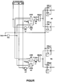
- the figure shows the structure of a circuit which is designed for this is that, if necessary, selectively only certain circuit parts be put into operation.
- the circuit which is described in more detail below Method and the device described in more detail below to test is an integrated logic circuit.
- the method and the device can also be non-integrated Circuits and / or circuits other than Logic circuits are tested.
- the method and the device serve in particular to the circuits at the manufacturer before they are delivered testing. Nevertheless, the method and the device also for one to be carried out later and elsewhere Verification are used.
- the method using which the circuit to be tested is tested is a scanning process, taking the elements the flip-flops of the circuit under test are.
- elements of the scan chain can also circuit parts other than flip-flops can be used.
- the circuit to be tested is used to carry out stage 1 placed in a scan mode in which the flip-flops connected in series in one or more scan chains are.
- clock pulses run times of different lengths from the clock generator the scan chain elements or when the clock pulses from Multiple clock generators are generated that are not exact initiated and / or operated simultaneously can be or if the signals that are connected in series Transfer scan chain elements are exceptionally long or short terms.
- the clock pulses, through which the scan chain elements can be clocked also be special test clock pulses.
- step 1 After initializing the scan chain elements in step 1 becomes the circuit under test to exit the scan mode causes the series connection the scan chain elements is lifted and the circuit can be operated normally as a test.
- the normal test operation differs significantly from that of conventional Test procedure. It won't be the entire circuit at once, but only a selected part at a time the same put into operation. Beyond, but completely independent of this becomes at least for clocking the scan chain elements uses a special test clock signal.
- the circuit parts, each put into operation simultaneously are, are or contain only such scan chain elements, that work together properly (then to Data reception are ready when data arrives or then data output when the receiver is ready to receive).
- This The procedure enables the current status reliably predict the scan chain elements the comparison carried out in step 4 of that determined in step 3 Current state of the scan chain elements with one a reliable theoretical or empirically determined target state Statement about the defectiveness or absence of errors of the circuit to be tested.
- Steps 3 and 4 can be carried out particularly easily and quickly if all of the circuit parts operated simultaneously Include elements of one or more scan chains.
- the arrangement shown in the figure shows from testing circuit just a few scan chain elements, more specifically said flip-flops FF1-1 to FF1-n of a first scan chain S1 and flip-flops FFn-1 to FFn-n of an nth scan chain Sn.
- Each the flip-flop has a clock signal input terminal C, an operating mode selection connection TE, a test input connection TI, a normal input port, not shown, and one Output connection O on.
- the clock signal input terminals C the flip-flops of a respective scan chain are included connected to the output terminal of a multiplexer.
- the Clock signal input terminals C of flip-flops FF1-1 to FF1-n the first scan chain S1 are with the multiplexer MUX1
- the clock signal input terminals C of the flip-flops FFn-1 to FFn-n of the nth scan chain Sn are with the multiplexer MUXn connected.
- the multiplexers have two input connections on, that clock signal at one of the input connections with which the respective flip-flops during of normal operation are clocked (CLK1 with MUX1 and CLKn at MUXn), and where the other of the input connections the multiplexer each has two AND gates AND11 and AND12 or ANDn1 and ANDn2 and two OR gates OR11 and OR12 or ORn1 and ORn2 existing logic circuit is connected upstream, which with an operating mode selection signal TES, with the contents of a scan chain selection register SCANSELREG (with the contents of register elements R1 to Rn and MS) and a test clock signal TCLK.
- the operating mode selection signal TES is active if and for as long steps 1 and 3 of the circuit test are carried out; it is inactive if and as long as step 2 of the circuit test is performed.
- the operating mode selection signal TES is also available in inverted form, with the Inversion is accomplished by an inverter INV.
- the content of the register element MS is high on if the test items are put into operation during the test Circuit all circuit parts put into operation simultaneously should be; it has a low level if only selected circuit parts put into operation at the same time should be.
- the register elements R1 to Rn one of which is one specific scan chain, more specifically the element R1 of the Scan chain S1, an element R2 of a scan chain S2, ..., and the element Rn is assigned to the scan chain Sn, insert (at low level of the register element MS) determines which of the Circuit parts of the circuit to be tested during the test Commissioning can be put into operation at the same time.
- the circuit to be tested is determined by the operating mode selection signal TES set to scan mode.
- the respective multiplexers do not more the normal clock signals CLK1 and CLKn to the clock signal input connections C of the flip-flops switched through, but the respective output signals of the other multiplexer input connections upstream logic circuits; Incidentally, this is also the case when the commissioning of the circuit to be tested in step 2 of the circuit test of Case.
- test clock signal does not become TCLK switched through.
- Which are the circuit parts that belong to a respective one Can be put into operation at the same time is preferably based on the layout of the test Switching taking into account the expected Taktskew and the expected data transit times between the scan chain elements fixed. There will only be such Scan chain elements put into operation at the same time as a test, in which the Taktskew between the individual bars is less than the shortest signal transit time between two Scan chain elements.
- the definition of operating simultaneously Circuit parts to be set can alternatively or additionally also take into account other conditions; what is important is "only" that the circuit parts under the given circumstances (test conditions) interact properly.
- the scan chain elements used in the example considered are put into operation at the same time all elements of one or more scan chains. That is, the Commissioning of the scan chain elements takes place in units of one or more scan chains. With appropriate modification the arrangement shown in the figure, however also arbitrarily selected elements of any scan chains together be put into operation.
- step 2 of the circuit test After selected circuit parts of the circuit to be tested briefly in step 2 of the circuit test (in the example considered for the duration of one cycle) in operation have been set, the circuit to be tested (by Activation of the operating mode selection signal TES) for execution from step 3 of the circuit test back to scan mode transferred.
- This will scan the chain elements again connected to the scan chains. This enables read out the respective states of the scan chain elements.
- the scan chains more precisely the elements of a respective scan chain all you have to do is initialize the Scan chain be clocked. This alone is enough to make the States of the respective scan chain elements or represent them Data or signals sequentially at the rear Push out the end of the relevant scan chain.
- step 1 Simultaneously with reading out the status of the scan chain elements can be reinitialized as in step 1.
- steps 1 to 4 of the circuit test with only partial test commissioning of the circuit under test repeated so many times have to be until all circuit parts at least once were put into operation as a test and thus a review could be subjected.
- the actual states read out in step 3 of the circuit test The scan chain elements are one in step 4 Subject to comparison with known target states.
- steps 1 to 4 there is a run of the circuit test ended. Not all circuit parts steps 1 to 4 or 2 to 4 be repeated for the circuit parts not yet tested.
- the scan chain selection register SCANSELREG be modified in content, in such a way that the so far not yet at least partially in the next run tested circuit parts are tested.
- step 2 of the described method also proves to be advantageous if the circuit parts initialized differently than in step 1 and / or their States different from those read in step 3. Especially it is not a mandatory requirement that those concerned Elements for this are connected in series to form chains become; instead, it can be provided, for example, address the individual elements for loading and unloading directly (e.g. via a parallel register transfer).
- test patterns the initial states, in which the individual circuit parts The start of the test or before each test run must be moved (the so-called test patterns), without considering one possibly existing in the circuit to be tested Taktskew can be designed, because this can be done at partial commissioning of the circuit under test to a negligible or tolerable extent be limited. This will design the test pattern considerably easier and less prone to errors than before was the case.
Landscapes
- Engineering & Computer Science (AREA)
- General Engineering & Computer Science (AREA)
- Physics & Mathematics (AREA)
- General Physics & Mathematics (AREA)
- Tests Of Electronic Circuits (AREA)
Applications Claiming Priority (2)
| Application Number | Priority Date | Filing Date | Title |
|---|---|---|---|
| DE19741212 | 1997-09-18 | ||
| DE19741212 | 1997-09-18 |
Publications (3)
| Publication Number | Publication Date |
|---|---|
| EP0903587A2 true EP0903587A2 (fr) | 1999-03-24 |
| EP0903587A3 EP0903587A3 (fr) | 1999-10-20 |
| EP0903587B1 EP0903587B1 (fr) | 2005-11-02 |
Family
ID=7842842
Family Applications (1)
| Application Number | Title | Priority Date | Filing Date |
|---|---|---|---|
| EP98115905A Expired - Lifetime EP0903587B1 (fr) | 1997-09-18 | 1998-08-24 | Procédé de test d'un circuit électronique |
Country Status (5)
| Country | Link |
|---|---|
| US (1) | US6308291B1 (fr) |
| EP (1) | EP0903587B1 (fr) |
| JP (1) | JPH11174129A (fr) |
| KR (1) | KR19990029918A (fr) |
| DE (1) | DE59813158D1 (fr) |
Cited By (1)
| Publication number | Priority date | Publication date | Assignee | Title |
|---|---|---|---|---|
| DE10112560A1 (de) * | 2001-03-15 | 2002-10-02 | Infineon Technologies Ag | Verfahren und Vorrichtung zum Prüfen von Schaltungsmodulen |
Families Citing this family (21)
| Publication number | Priority date | Publication date | Assignee | Title |
|---|---|---|---|---|
| EP1145159A3 (fr) * | 1998-09-30 | 2002-07-10 | Cadence Design Systems, Inc. | Methodologie de construction fondee sur des blocs |
| US8533547B2 (en) | 1999-11-23 | 2013-09-10 | Mentor Graphics Corporation | Continuous application and decompression of test patterns and selective compaction of test responses |
| US9134370B2 (en) | 1999-11-23 | 2015-09-15 | Mentor Graphics Corporation | Continuous application and decompression of test patterns and selective compaction of test responses |
| US9664739B2 (en) | 1999-11-23 | 2017-05-30 | Mentor Graphics Corporation | Continuous application and decompression of test patterns and selective compaction of test responses |
| US7493540B1 (en) | 1999-11-23 | 2009-02-17 | Jansuz Rajski | Continuous application and decompression of test patterns to a circuit-under-test |
| US6327687B1 (en) | 1999-11-23 | 2001-12-04 | Janusz Rajski | Test pattern compression for an integrated circuit test environment |
| US6353842B1 (en) * | 1999-11-23 | 2002-03-05 | Janusz Rajski | Method for synthesizing linear finite state machines |
| JP3845016B2 (ja) | 1999-11-23 | 2006-11-15 | メンター・グラフィクス・コーポレーション | テスト中回路技術分野へのテストパターンの連続的な適用およびデコンプレッション |
| US6557129B1 (en) | 1999-11-23 | 2003-04-29 | Janusz Rajski | Method and apparatus for selectively compacting test responses |
| US6684358B1 (en) | 1999-11-23 | 2004-01-27 | Janusz Rajski | Decompressor/PRPG for applying pseudo-random and deterministic test patterns |
| US6874109B1 (en) | 1999-11-23 | 2005-03-29 | Janusz Rajski | Phase shifter with reduced linear dependency |
| US6715091B1 (en) * | 2000-04-10 | 2004-03-30 | Intel Corporation | System for rearranging plurality of memory storage elements in a computer process to different configuration upon entry into a low power mode of operation |
| JP4480238B2 (ja) * | 2000-07-18 | 2010-06-16 | Okiセミコンダクタ株式会社 | 半導体装置 |
| US6671847B1 (en) * | 2000-11-08 | 2003-12-30 | Intel Corporation | I/O device testing method and apparatus |
| US7302624B2 (en) * | 2003-02-13 | 2007-11-27 | Janusz Rajski | Adaptive fault diagnosis of compressed test responses |
| WO2004072660A2 (fr) * | 2003-02-13 | 2004-08-26 | Mentor Graphics Corporation | Compression de reponses a des tests au moyen d'un compacteur |
| US7437640B2 (en) * | 2003-02-13 | 2008-10-14 | Janusz Rajski | Fault diagnosis of compressed test responses having one or more unknown states |
| US7509550B2 (en) * | 2003-02-13 | 2009-03-24 | Janusz Rajski | Fault diagnosis of compressed test responses |
| US7296249B2 (en) * | 2003-10-10 | 2007-11-13 | Thomas Hans Rinderknecht | Using constrained scan cells to test integrated circuits |
| US8793545B2 (en) | 2012-07-03 | 2014-07-29 | Apple Inc. | Apparatus and method for clock glitch detection during at-speed testing |
| WO2021045769A1 (fr) * | 2019-09-06 | 2021-03-11 | Siemens Industry Software Inc. | Architecture de compacteur universelle pour circuits de test |
Family Cites Families (16)
| Publication number | Priority date | Publication date | Assignee | Title |
|---|---|---|---|---|
| GB8432533D0 (en) | 1984-12-21 | 1985-02-06 | Plessey Co Plc | Integrated circuits |
| DE3732830A1 (de) | 1987-09-29 | 1989-04-06 | Siemens Ag | Schaltungsanordnung zur pruefung der funktionsfaehigkeit einer komplexen schaltung |
| US4897836A (en) | 1987-10-20 | 1990-01-30 | Gazelle Microcircuits, Inc. | Programmable connection path circuit |
| DE3886529T2 (de) * | 1988-08-27 | 1994-06-30 | Ibm | Einrichtung in einem Datenverarbeitungssystem zur System-Initialisierung und -Rückstellung. |
| US5271019A (en) * | 1991-03-15 | 1993-12-14 | Amdahl Corporation | Scannable system with addressable scan reset groups |
| US5349587A (en) * | 1992-03-26 | 1994-09-20 | Northern Telecom Limited | Multiple clock rate test apparatus for testing digital systems |
| US5365528A (en) * | 1992-04-03 | 1994-11-15 | At&T Bell Laboratories | Method for testing delay faults in non-scan sequential circuits |
| TW253942B (fr) * | 1994-01-31 | 1995-08-11 | At & T Corp | |
| JP2624169B2 (ja) * | 1994-04-15 | 1997-06-25 | 日本電気株式会社 | スキャンパスを有する論理集積回路 |
| US5617427A (en) * | 1994-10-18 | 1997-04-01 | Matsushita Electcric Industrial Co., Ltd. | Method for generating test sequences for detecting faults in target scan logical blocks |
| US5717700A (en) * | 1995-12-04 | 1998-02-10 | Motorola, Inc. | Method for creating a high speed scan-interconnected set of flip-flop elements in an integrated circuit to enable faster scan-based testing |
| JPH09197015A (ja) * | 1996-01-19 | 1997-07-31 | Nec Corp | 大規模回路テスト方式 |
| US5812561A (en) * | 1996-09-03 | 1998-09-22 | Motorola, Inc. | Scan based testing of an integrated circuit for compliance with timing specifications |
| KR100206124B1 (ko) * | 1996-10-14 | 1999-07-01 | 윤종용 | 자기테스트회로 |
| US5761215A (en) * | 1997-06-03 | 1998-06-02 | Motorola, Inc. | Scan based path delay testing of integrated circuits containing embedded memory elements |
| US6065145A (en) * | 1998-04-13 | 2000-05-16 | Lucent Technologies, Inc. | Method for testing path delay faults in sequential logic circuits |
-
1998
- 1998-08-24 EP EP98115905A patent/EP0903587B1/fr not_active Expired - Lifetime
- 1998-08-24 DE DE59813158T patent/DE59813158D1/de not_active Expired - Lifetime
- 1998-09-17 JP JP10263008A patent/JPH11174129A/ja active Pending
- 1998-09-18 KR KR1019980038612A patent/KR19990029918A/ko not_active Ceased
- 1998-09-18 US US09/156,442 patent/US6308291B1/en not_active Expired - Lifetime
Cited By (2)
| Publication number | Priority date | Publication date | Assignee | Title |
|---|---|---|---|---|
| DE10112560A1 (de) * | 2001-03-15 | 2002-10-02 | Infineon Technologies Ag | Verfahren und Vorrichtung zum Prüfen von Schaltungsmodulen |
| DE10112560B4 (de) * | 2001-03-15 | 2011-02-17 | Infineon Technologies Ag | Verfahren und Vorrichtung zum Prüfen von Schaltungsmodulen |
Also Published As
| Publication number | Publication date |
|---|---|
| EP0903587A3 (fr) | 1999-10-20 |
| DE59813158D1 (de) | 2005-12-08 |
| US6308291B1 (en) | 2001-10-23 |
| KR19990029918A (ko) | 1999-04-26 |
| EP0903587B1 (fr) | 2005-11-02 |
| JPH11174129A (ja) | 1999-07-02 |
Similar Documents
| Publication | Publication Date | Title |
|---|---|---|
| EP0903587B1 (fr) | Procédé de test d'un circuit électronique | |
| DE3882266T2 (de) | Abfrageprüfgerät für digitale Systeme mit dynamischem Direktzugriffspeicher. | |
| EP1097460B1 (fr) | Circuit integre comportant pour son autocontrole un dispositif d'autoverification | |
| DE69732960T2 (de) | Integrierte schaltung mit einer ersten und zweiten taktdomäne und prüfvorrichtung für eine solche schaltung | |
| DE3700251C2 (fr) | ||
| EP0144078A2 (fr) | Méthode et agencement de test d'un circuit à l'aide d'une voie d'exploration | |
| DE3702408C2 (fr) | ||
| EP0009572A2 (fr) | Méthode et dispositif pour le test de circuits séquentiels réalisés en circuits semi-conducteurs qui sont monolithiquement intégrés | |
| DE69023674T2 (de) | Verfahren zur Prüfung einer Schaltung sowie geeignete Schaltung für ein derartiges Verfahren. | |
| DE3124902C2 (fr) | ||
| DE19738569A1 (de) | Testschaltkreis für integrierte Schaltkreise | |
| DE10150321A1 (de) | Verfahren und Vorrichtung zum Testen von integrierten Schaltungen | |
| DE69217524T2 (de) | Testschaltung, vorgesehen in digitalen logischen Schaltungen | |
| EP0186724A1 (fr) | Dispositif de test et de diagnostic pour une calculatrice numérique | |
| DE60109321T2 (de) | Prüfung von asynchroner rücksetzschaltung | |
| DE4404445A1 (de) | Integrierte Halbleiterschaltung und Verfahren zum Testen derselben | |
| DE69116663T2 (de) | Integrierter Schaltkreis mit Peripherieprüfungssteuerung | |
| DE19903606B4 (de) | Halbleiteranordnung | |
| DE3817143C2 (fr) | ||
| DE69833123T2 (de) | Schaltungsanordnung zum testen eines kerns | |
| DE60112723T2 (de) | Lssd schnittstelle | |
| DE102008003450A1 (de) | Digitalschaltungen und Verfahren zum Testen einer Digitalschaltung | |
| EP1504273B1 (fr) | Systeme pour tester des modules numeriques | |
| DE68928600T2 (de) | Erweiterte Prüfschaltung | |
| EP1182555B1 (fr) | Procédé de test d'un microcontrolleur à l'aide d'un dispositif de test externe |
Legal Events
| Date | Code | Title | Description |
|---|---|---|---|
| PUAI | Public reference made under article 153(3) epc to a published international application that has entered the european phase |
Free format text: ORIGINAL CODE: 0009012 |
|
| AK | Designated contracting states |
Kind code of ref document: A2 Designated state(s): DE FR GB IT |
|
| AX | Request for extension of the european patent |
Free format text: AL;LT;LV;MK;RO;SI |
|
| PUAL | Search report despatched |
Free format text: ORIGINAL CODE: 0009013 |
|
| AK | Designated contracting states |
Kind code of ref document: A3 Designated state(s): AT BE CH CY DE DK ES FI FR GB GR IE IT LI LU MC NL PT SE |
|
| AX | Request for extension of the european patent |
Free format text: AL;LT;LV;MK;RO;SI |
|
| 17P | Request for examination filed |
Effective date: 19991118 |
|
| AKX | Designation fees paid |
Free format text: DE FR GB IT |
|
| RAP1 | Party data changed (applicant data changed or rights of an application transferred) |
Owner name: INFINEON TECHNOLOGIES AG |
|
| 17Q | First examination report despatched |
Effective date: 20040506 |
|
| GRAP | Despatch of communication of intention to grant a patent |
Free format text: ORIGINAL CODE: EPIDOSNIGR1 |
|
| GRAS | Grant fee paid |
Free format text: ORIGINAL CODE: EPIDOSNIGR3 |
|
| GRAA | (expected) grant |
Free format text: ORIGINAL CODE: 0009210 |
|
| AK | Designated contracting states |
Kind code of ref document: B1 Designated state(s): DE FR GB IT |
|
| PG25 | Lapsed in a contracting state [announced via postgrant information from national office to epo] |
Ref country code: IT Free format text: LAPSE BECAUSE OF FAILURE TO SUBMIT A TRANSLATION OF THE DESCRIPTION OR TO PAY THE FEE WITHIN THE PRESCRIBED TIME-LIMIT;WARNING: LAPSES OF ITALIAN PATENTS WITH EFFECTIVE DATE BEFORE 2007 MAY HAVE OCCURRED AT ANY TIME BEFORE 2007. THE CORRECT EFFECTIVE DATE MAY BE DIFFERENT FROM THE ONE RECORDED. Effective date: 20051102 Ref country code: GB Free format text: LAPSE BECAUSE OF FAILURE TO SUBMIT A TRANSLATION OF THE DESCRIPTION OR TO PAY THE FEE WITHIN THE PRESCRIBED TIME-LIMIT Effective date: 20051102 |
|
| REG | Reference to a national code |
Ref country code: GB Ref legal event code: FG4D Free format text: NOT ENGLISH |
|
| REF | Corresponds to: |
Ref document number: 59813158 Country of ref document: DE Date of ref document: 20051208 Kind code of ref document: P |
|
| GBV | Gb: ep patent (uk) treated as always having been void in accordance with gb section 77(7)/1977 [no translation filed] |
Effective date: 20051102 |
|
| ET | Fr: translation filed | ||
| PLBE | No opposition filed within time limit |
Free format text: ORIGINAL CODE: 0009261 |
|
| STAA | Information on the status of an ep patent application or granted ep patent |
Free format text: STATUS: NO OPPOSITION FILED WITHIN TIME LIMIT |
|
| 26N | No opposition filed |
Effective date: 20060803 |
|
| REG | Reference to a national code |
Ref country code: FR Ref legal event code: PLFP Year of fee payment: 19 |
|
| PGFP | Annual fee paid to national office [announced via postgrant information from national office to epo] |
Ref country code: FR Payment date: 20160822 Year of fee payment: 19 |
|
| PGFP | Annual fee paid to national office [announced via postgrant information from national office to epo] |
Ref country code: DE Payment date: 20161020 Year of fee payment: 19 |
|
| REG | Reference to a national code |
Ref country code: DE Ref legal event code: R119 Ref document number: 59813158 Country of ref document: DE |
|
| REG | Reference to a national code |
Ref country code: FR Ref legal event code: ST Effective date: 20180430 |
|
| PG25 | Lapsed in a contracting state [announced via postgrant information from national office to epo] |
Ref country code: DE Free format text: LAPSE BECAUSE OF NON-PAYMENT OF DUE FEES Effective date: 20180301 |
|
| PG25 | Lapsed in a contracting state [announced via postgrant information from national office to epo] |
Ref country code: FR Free format text: LAPSE BECAUSE OF NON-PAYMENT OF DUE FEES Effective date: 20170831 |