EP0903587A2 - Test method for an electronic circuit - Google Patents
Test method for an electronic circuit Download PDFInfo
- Publication number
- EP0903587A2 EP0903587A2 EP98115905A EP98115905A EP0903587A2 EP 0903587 A2 EP0903587 A2 EP 0903587A2 EP 98115905 A EP98115905 A EP 98115905A EP 98115905 A EP98115905 A EP 98115905A EP 0903587 A2 EP0903587 A2 EP 0903587A2
- Authority
- EP
- European Patent Office
- Prior art keywords
- circuit
- test
- scan chain
- circuit parts
- scan
- Prior art date
- Legal status (The legal status is an assumption and is not a legal conclusion. Google has not performed a legal analysis and makes no representation as to the accuracy of the status listed.)
- Granted
Links
- 238000010998 test method Methods 0.000 title description 2
- 238000012360 testing method Methods 0.000 claims abstract description 78
- 238000000034 method Methods 0.000 claims abstract description 32
- 230000003993 interaction Effects 0.000 claims description 3
- 230000001419 dependent effect Effects 0.000 claims 1
- 230000008569 process Effects 0.000 description 4
- 102100040862 Dual specificity protein kinase CLK1 Human genes 0.000 description 2
- 101000749294 Homo sapiens Dual specificity protein kinase CLK1 Proteins 0.000 description 2
- 238000012552 review Methods 0.000 description 2
- 238000012546 transfer Methods 0.000 description 2
- 238000011144 upstream manufacturing Methods 0.000 description 2
- 101100491597 Neurospora crassa (strain ATCC 24698 / 74-OR23-1A / CBS 708.71 / DSM 1257 / FGSC 987) arg-6 gene Proteins 0.000 description 1
- 230000004913 activation Effects 0.000 description 1
- 230000008859 change Effects 0.000 description 1
- 238000010276 construction Methods 0.000 description 1
- 238000013461 design Methods 0.000 description 1
- 238000011161 development Methods 0.000 description 1
- 230000018109 developmental process Effects 0.000 description 1
- 238000011156 evaluation Methods 0.000 description 1
- 238000012986 modification Methods 0.000 description 1
- 230000004048 modification Effects 0.000 description 1
- 230000004044 response Effects 0.000 description 1
- 238000012795 verification Methods 0.000 description 1
Images
Classifications
-
- G—PHYSICS
- G01—MEASURING; TESTING
- G01R—MEASURING ELECTRIC VARIABLES; MEASURING MAGNETIC VARIABLES
- G01R31/00—Arrangements for testing electric properties; Arrangements for locating electric faults; Arrangements for electrical testing characterised by what is being tested not provided for elsewhere
- G01R31/28—Testing of electronic circuits, e.g. by signal tracer
- G01R31/317—Testing of digital circuits
- G01R31/3181—Functional testing
- G01R31/3185—Reconfiguring for testing, e.g. LSSD, partitioning
- G01R31/318533—Reconfiguring for testing, e.g. LSSD, partitioning using scanning techniques, e.g. LSSD, Boundary Scan, JTAG
- G01R31/318558—Addressing or selecting of subparts of the device under test
- G01R31/318563—Multiple simultaneous testing of subparts
Definitions
- the present invention relates to a method according to the Preamble of claim 1, i.e. a procedure for Testing an electronic circuit in which the current state from before after an initial initialization circuit parts put into operation with a test Target state is compared.
- Such a method is, in particular, for example so-called used for testing integrated circuits Scanning process.
- the circuits that are tested according to the scanning process must be able to be put into a scan mode be in which selected circuit parts such as all flip-flops of the circuit are connected so that it by one provided outside the circuit to be tested Test facility individually in certain initial states are relocatable and that their current state if necessary can be read out by the test device.
- This can in the case of using flip-flops as selected circuit parts can be achieved in that the flip-flops in the Scan mode are connected in series, whereby the input terminal of a respective flip-flop with the Output connection of the flip-flop in the row in front of it is connected, and wherein the output terminal is a respective flip-flops with the input terminal of the in the Row flip-flops coming after it is connected.
- Such Arrangement is also called a scan chain.
- Such a scan chain more precisely the one under consideration
- Example elements formed by flip-flops can be relative just be initialized.
- One at the input port of the signal applied to the first flip-flops of the scan chain, more precisely said in response to the state of the relevant flip-flops is namely with the clock one the flip-flops applied clock signal from flip-flop to flip-flop pushed on; every flip-flop of the scan chain takes with every clock pulse the state of in the scan chain pending flip-flops.
- the test of the Switching according to the scanning process as follows: First, the circuit is set to scan mode, which results in forms the aforementioned scan chain. This scan chain is through sequential application of n input signals and n clock pulses placed in a defined initial state. After that the circuit is placed in a normal mode; the To do this, scan mode is exited, the scan chain (the Series connection of the flip-flops) resolved. In normal mode the circuit becomes normal for a short test operated. The duration during which the circuit is normal is preferably operated by a number of clock cycles Are defined. This number of clock cycles is preferred very small (e.g. 1).
- the present invention is therefore based on the object the method according to the preamble of claim 1 to further develop such that only faulty circuits are classified as faulty.
- circuit parts to be tested essentially only such circuit parts operated simultaneously, of which among the given Under certain circumstances, an intended interaction is expected can.
- a designated cooperation of cooperating Circuit parts which, for example, the flip-flops, however also other and / or more extensive components of those to be tested Circuit may not be, among other things, then expect when the clock signals with which the individual Circuit parts are to be clocked during test operation during of the circuit test an excessive mutual offset or have Taktskew. This is usually special pronounced when the clock signals by different clock signal generators be generated.
- circuit parts not put into operation are preferred "only" not supplied with clock signals.
- circuit part states With such a partial operation of the circuit you always get exactly reproducible results (circuit part states); that the interested and the evaluation of the test were based States of the circuit parts (of the elements a scan chain) can vary randomly, is reliably excluded.
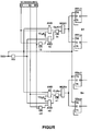
- the figure shows the structure of a circuit which is designed for this is that, if necessary, selectively only certain circuit parts be put into operation.
- the circuit which is described in more detail below Method and the device described in more detail below to test is an integrated logic circuit.
- the method and the device can also be non-integrated Circuits and / or circuits other than Logic circuits are tested.
- the method and the device serve in particular to the circuits at the manufacturer before they are delivered testing. Nevertheless, the method and the device also for one to be carried out later and elsewhere Verification are used.
- the method using which the circuit to be tested is tested is a scanning process, taking the elements the flip-flops of the circuit under test are.
- elements of the scan chain can also circuit parts other than flip-flops can be used.
- the circuit to be tested is used to carry out stage 1 placed in a scan mode in which the flip-flops connected in series in one or more scan chains are.
- clock pulses run times of different lengths from the clock generator the scan chain elements or when the clock pulses from Multiple clock generators are generated that are not exact initiated and / or operated simultaneously can be or if the signals that are connected in series Transfer scan chain elements are exceptionally long or short terms.
- the clock pulses, through which the scan chain elements can be clocked also be special test clock pulses.
- step 1 After initializing the scan chain elements in step 1 becomes the circuit under test to exit the scan mode causes the series connection the scan chain elements is lifted and the circuit can be operated normally as a test.
- the normal test operation differs significantly from that of conventional Test procedure. It won't be the entire circuit at once, but only a selected part at a time the same put into operation. Beyond, but completely independent of this becomes at least for clocking the scan chain elements uses a special test clock signal.
- the circuit parts, each put into operation simultaneously are, are or contain only such scan chain elements, that work together properly (then to Data reception are ready when data arrives or then data output when the receiver is ready to receive).
- This The procedure enables the current status reliably predict the scan chain elements the comparison carried out in step 4 of that determined in step 3 Current state of the scan chain elements with one a reliable theoretical or empirically determined target state Statement about the defectiveness or absence of errors of the circuit to be tested.
- Steps 3 and 4 can be carried out particularly easily and quickly if all of the circuit parts operated simultaneously Include elements of one or more scan chains.
- the arrangement shown in the figure shows from testing circuit just a few scan chain elements, more specifically said flip-flops FF1-1 to FF1-n of a first scan chain S1 and flip-flops FFn-1 to FFn-n of an nth scan chain Sn.
- Each the flip-flop has a clock signal input terminal C, an operating mode selection connection TE, a test input connection TI, a normal input port, not shown, and one Output connection O on.
- the clock signal input terminals C the flip-flops of a respective scan chain are included connected to the output terminal of a multiplexer.
- the Clock signal input terminals C of flip-flops FF1-1 to FF1-n the first scan chain S1 are with the multiplexer MUX1
- the clock signal input terminals C of the flip-flops FFn-1 to FFn-n of the nth scan chain Sn are with the multiplexer MUXn connected.
- the multiplexers have two input connections on, that clock signal at one of the input connections with which the respective flip-flops during of normal operation are clocked (CLK1 with MUX1 and CLKn at MUXn), and where the other of the input connections the multiplexer each has two AND gates AND11 and AND12 or ANDn1 and ANDn2 and two OR gates OR11 and OR12 or ORn1 and ORn2 existing logic circuit is connected upstream, which with an operating mode selection signal TES, with the contents of a scan chain selection register SCANSELREG (with the contents of register elements R1 to Rn and MS) and a test clock signal TCLK.
- the operating mode selection signal TES is active if and for as long steps 1 and 3 of the circuit test are carried out; it is inactive if and as long as step 2 of the circuit test is performed.
- the operating mode selection signal TES is also available in inverted form, with the Inversion is accomplished by an inverter INV.
- the content of the register element MS is high on if the test items are put into operation during the test Circuit all circuit parts put into operation simultaneously should be; it has a low level if only selected circuit parts put into operation at the same time should be.
- the register elements R1 to Rn one of which is one specific scan chain, more specifically the element R1 of the Scan chain S1, an element R2 of a scan chain S2, ..., and the element Rn is assigned to the scan chain Sn, insert (at low level of the register element MS) determines which of the Circuit parts of the circuit to be tested during the test Commissioning can be put into operation at the same time.
- the circuit to be tested is determined by the operating mode selection signal TES set to scan mode.
- the respective multiplexers do not more the normal clock signals CLK1 and CLKn to the clock signal input connections C of the flip-flops switched through, but the respective output signals of the other multiplexer input connections upstream logic circuits; Incidentally, this is also the case when the commissioning of the circuit to be tested in step 2 of the circuit test of Case.
- test clock signal does not become TCLK switched through.
- Which are the circuit parts that belong to a respective one Can be put into operation at the same time is preferably based on the layout of the test Switching taking into account the expected Taktskew and the expected data transit times between the scan chain elements fixed. There will only be such Scan chain elements put into operation at the same time as a test, in which the Taktskew between the individual bars is less than the shortest signal transit time between two Scan chain elements.
- the definition of operating simultaneously Circuit parts to be set can alternatively or additionally also take into account other conditions; what is important is "only" that the circuit parts under the given circumstances (test conditions) interact properly.
- the scan chain elements used in the example considered are put into operation at the same time all elements of one or more scan chains. That is, the Commissioning of the scan chain elements takes place in units of one or more scan chains. With appropriate modification the arrangement shown in the figure, however also arbitrarily selected elements of any scan chains together be put into operation.
- step 2 of the circuit test After selected circuit parts of the circuit to be tested briefly in step 2 of the circuit test (in the example considered for the duration of one cycle) in operation have been set, the circuit to be tested (by Activation of the operating mode selection signal TES) for execution from step 3 of the circuit test back to scan mode transferred.
- This will scan the chain elements again connected to the scan chains. This enables read out the respective states of the scan chain elements.
- the scan chains more precisely the elements of a respective scan chain all you have to do is initialize the Scan chain be clocked. This alone is enough to make the States of the respective scan chain elements or represent them Data or signals sequentially at the rear Push out the end of the relevant scan chain.
- step 1 Simultaneously with reading out the status of the scan chain elements can be reinitialized as in step 1.
- steps 1 to 4 of the circuit test with only partial test commissioning of the circuit under test repeated so many times have to be until all circuit parts at least once were put into operation as a test and thus a review could be subjected.
- the actual states read out in step 3 of the circuit test The scan chain elements are one in step 4 Subject to comparison with known target states.
- steps 1 to 4 there is a run of the circuit test ended. Not all circuit parts steps 1 to 4 or 2 to 4 be repeated for the circuit parts not yet tested.
- the scan chain selection register SCANSELREG be modified in content, in such a way that the so far not yet at least partially in the next run tested circuit parts are tested.
- step 2 of the described method also proves to be advantageous if the circuit parts initialized differently than in step 1 and / or their States different from those read in step 3. Especially it is not a mandatory requirement that those concerned Elements for this are connected in series to form chains become; instead, it can be provided, for example, address the individual elements for loading and unloading directly (e.g. via a parallel register transfer).
- test patterns the initial states, in which the individual circuit parts The start of the test or before each test run must be moved (the so-called test patterns), without considering one possibly existing in the circuit to be tested Taktskew can be designed, because this can be done at partial commissioning of the circuit under test to a negligible or tolerable extent be limited. This will design the test pattern considerably easier and less prone to errors than before was the case.
Landscapes
- Engineering & Computer Science (AREA)
- General Engineering & Computer Science (AREA)
- Physics & Mathematics (AREA)
- General Physics & Mathematics (AREA)
- Tests Of Electronic Circuits (AREA)
Abstract
Es wird ein Verfahren zum Testen einer elektronischen Schaltung
beschrieben, bei welchem der Ist-Zustand von zuvor nach
einer anfänglichen Initialisierung testweise in Betrieb gesetzten
Schaltungsteilen mit einem Soll-Zustand verglichen
wird. Das beschriebene Verfahren zeichnet sich dadurch aus,
daß von den zu testenden Schaltungsteilen im wesentlichen nur
jeweils solche Schaltungsteile gleichzeitig betrieben werden,
von denen unter den gegebenen Umständen ein bestimmungsgemäßes
Zusammenwirken erwartet werden kann.

Description
Die vorliegende Erfindung betrifft ein Verfahren gemäß dem
Oberbegriff des Patentanspruchs 1, d.h. ein Verfahren zum
Testen einer elektronischen Schaltung, bei welchem der Ist-Zustand
von zuvor nach einer anfänglichen Initialisierung
testweise in Betrieb gesetzten Schaltungsteilen mit einem
Soll-Zustand verglichen wird.The present invention relates to a method according to the
Preamble of
Ein derartiges Verfahren ist beispielsweise das insbesondere zum Testen integrierter Schaltungen verwendete sogenannte Scan-Verfahren.Such a method is, in particular, for example so-called used for testing integrated circuits Scanning process.
Die Schaltungen, die nach dem Scan-Verfahren getestet werden können sollen, müssen in eine Scan-Betriebsart versetzbar sein, in welcher ausgewählte Schaltungsteile wie beispielsweise alle Flip-Flops der Schaltung so verschaltet sind, daß sie durch eine außerhalb der zu testenden Schaltung vorgesehene Testeinrichtung individuell in bestimmte Anfangszustände versetzbar sind und daß deren aktueller Zustand bei Bedarf durch die Testeinrichtung ausgelesen werden kann. Dies kann im Fall der Verwendung von Flip-Flops als ausgewählte Schaltungsteile dadurch erreicht werden, daß die Flip-Flops in der Scan-Betriebsart in Reihe hintereinandergeschaltet sind, wobei der Eingangsanschluß eines jeweiligen Flip-Flops mit dem Ausgangsanschluß des in der Reihe vor ihm stehenden Flip-Flops verbunden ist, und wobei der Ausgangsanschluß eines jeweiligen Flip-Flops mit dem Eingangsanschluß des in der Reihe nach ihm kommenden Flip-Flops verbunden ist. Eine derartige Anordnung wird auch als Scan-Kette bezeichnet.The circuits that are tested according to the scanning process must be able to be put into a scan mode be in which selected circuit parts such as all flip-flops of the circuit are connected so that it by one provided outside the circuit to be tested Test facility individually in certain initial states are relocatable and that their current state if necessary can be read out by the test device. This can in the case of using flip-flops as selected circuit parts can be achieved in that the flip-flops in the Scan mode are connected in series, whereby the input terminal of a respective flip-flop with the Output connection of the flip-flop in the row in front of it is connected, and wherein the output terminal is a respective flip-flops with the input terminal of the in the Row flip-flops coming after it is connected. Such Arrangement is also called a scan chain.
Eine solche Scan-Kette, genauer gesagt deren im betrachteten Beispiel durch Flip-Flops gebildeten Elemente können relativ einfach initialisiert werden. Ein an den Eingangsanschluß des ersten Flip-Flops der Scan-Kette angelegtes Signal, genauer gesagt der sich im Ansprechen darauf einstellende Zustand des betreffenden Flip-Flops wird nämlich mit dem Takt eines an die Flip-Flops angelegten Taktsignals von Flip-Flop zu Flip-Flop weitergeschoben; jedes Flip-Flop der Scan-Kette nimmt mit jedem Taktimpuls den Zustand des in der Scan-Kette vor ihm stehenden Flip-Flops an.Such a scan chain, more precisely the one under consideration Example elements formed by flip-flops can be relative just be initialized. One at the input port of the signal applied to the first flip-flops of the scan chain, more precisely said in response to the state of the relevant flip-flops is namely with the clock one the flip-flops applied clock signal from flip-flop to flip-flop pushed on; every flip-flop of the scan chain takes with every clock pulse the state of in the scan chain pending flip-flops.
Soll das x-te Flip-Flop der Scan-Kette in den Zustand A versetzt werden, so muß "nur" an den Eingangsanschluß des ersten Flip-Flops der Scan-Kette ein Signal angelegt werden, durch welches dieses Flip-Flop und die nachgeschalteten Flip-Flops in den Zustand A versetzbar sind, und die Scan-Kette (alle Flip-Flops derselben) mit x Taktimpulsen beaufschlagt werden.Should the xth flip-flop of the scan chain be set to state A. , "only" must be connected to the input connection of the first Flip-flops of the scan chain can be applied to a signal which this flip-flop and the downstream flip-flops can be put into state A, and the scan chain (all Flip-flops of the same) are applied with x clock pulses.
Umgekehrt können am letzten Flip-Flop der Scan-Kette die Zustände der einzelnen Flip-Flops zu einem bestimmten Zeitpunkt sequentiell ausgelesen werden.Conversely, the states at the last flip-flop of the scan chain of the individual flip-flops at a certain point in time be read out sequentially.
Enthält die Scan-Kette n Flip-Flops, so läuft der Test der Schaltung nach dem Scan-Verfahren wie folgt ab: Zunächst wird die Schaltung in die Scan-Betriebsart versetzt, wodurch sich die erwähnte Scan-Kette bildet. Diese Scan-Kette wird durch sequentielles Anlegen von n Eingangssignalen und n Taktimpulsen in einen definierten Anfangszustand versetzt. Danach wird die Schaltung in eine Normal-Betriebsart versetzt; die Scan-Betriebsart wird hierzu verlassen, die Scan-Kette (die Reihenschaltung der Flip-Flops) aufgelöst. In der Normal-Betriebsart wird die Schaltung kurzzeitig testweise normal betrieben. Die Dauer, während welcher die Schaltung normal betrieben wird, wird vorzugsweise durch eine Anzahl von Taktzyklen definiert. Diese Anzahl von Taktzyklen ist vorzugsweise sehr klein (beispielsweise 1). In der Zeit, während welcher die Schaltung normal betrieben wird, verändern sich zumindest teilweise die Zustände der anfänglich initialisierten Flip-Flops, wobei es sich aus der bestimmungsgemäßen Funktion der zu testenden Schaltung ermitteln läßt, in welchem (Soll-)Zustand die Flip-Flops sich zu einem jeweiligen Zeitpunkt befinden müßten. Nachdem die Schaltung eine vorbestimmte Anzahl von Taktzyklen normal betrieben wurde, wird sie in die Scan-Betriebsart zurückversetzt, wodurch die Flip-Flops wieder zur Scan-Kette verschaltet werden. Werden die so verschalteten Flip-Flops in diesem Zustand mit Taktsignalen beaufschlagt, so werden am Ende der Scan-Kette (aus dem Ausgangsanschluß des letzten Flip-Flops der Scan-Kette) sequentiell im Takt der Taktsignale Daten herausgeschoben, welche den (Ist-)Zustand der Flip-Flops der Scan-Kette zum Zeitpunkt des Endes des Normal-Betriebs repräsentieren. Vergleicht man sodann den wie beschrieben ermittelten Ist-Zustand der Flip-Flops der Scan-Kette mit dem bekannten Soll-Zustand derselben, so läßt sich daran ersehen, ob die zu testende Schaltung fehlerfrei läuft oder nicht.If the scan chain contains n flip-flops, the test of the Switching according to the scanning process as follows: First, the circuit is set to scan mode, which results in forms the aforementioned scan chain. This scan chain is through sequential application of n input signals and n clock pulses placed in a defined initial state. After that the circuit is placed in a normal mode; the To do this, scan mode is exited, the scan chain (the Series connection of the flip-flops) resolved. In normal mode the circuit becomes normal for a short test operated. The duration during which the circuit is normal is preferably operated by a number of clock cycles Are defined. This number of clock cycles is preferred very small (e.g. 1). In time while which the circuit is operated normally change at least partially the states of the initially initialized Flip-flops, it being from the intended Function of the circuit to be tested can determine in which (Target) state of the flip-flops to a respective one Should be at the time. After the circuit has a predetermined Number of clock cycles was operated normally it put back into the scan mode, causing the flip-flops can be connected to the scan chain again. Are they like this? connected flip-flops in this state with clock signals , at the end of the scan chain (from the output connection of the last flip-flop in the scan chain) sequentially data pushed out in time with the clock signals, which the (actual) state of the flip-flops of the scan chain at the time represent the end of normal operation. If you compare then the actual state of the flip-flops determined as described the scan chain with the known target state of the same, so it can be seen whether the circuit to be tested runs flawlessly or not.
Derart oder ähnlich funktionierende Tests ermöglichen es auf relativ einfache Weise, selbst sehr komplexe Schaltungen innerhalb von sehr kurzer Zeit umfassend zu testen. Allerdings zeigt die Erfahrung, daß es unter ungünstigen Bedingungen vorkommen kann, daß ordnungsgemäß funktionierende Schaltungen als fehlerhaft eingestuft werden. Dies ist verständlicherweise ein Nachteil, den es zu beseitigen gilt.Such or similarly functioning tests make it possible relatively simple way, even very complex circuits to be tested comprehensively within a very short time. Indeed experience shows that it is under unfavorable conditions can happen that it works properly Circuits are classified as faulty. This is understandably a disadvantage that needs to be remedied.
Der vorliegenden Erfindung liegt daher die Aufgabe zugrunde,
das Verfahren gemäß dem Oberbegriff des Patentanspruchs 1
derart weiterzubilden, daß dadurch nur fehlerhafte Schaltungen
als fehlerhaft eingestuft werden.The present invention is therefore based on the object
the method according to the preamble of
Diese Aufgabe wird erfindungsgemäß durch die im kennzeichnenden
Teil des Patentanspruchs 1 beanspruchten Merkmale gelöst.This object is achieved by the characterizing
Part of
Demnach ist vorgesehen, daß von den zu testenden Schaltungsteilen im wesentlichen nur jeweils solche Schaltungsteile gleichzeitig betrieben werden, von denen unter den gegebenen Umständen ein bestimmungsgemäßes Zusammenwirken erwartet werden kann. Accordingly, it is provided that of the circuit parts to be tested essentially only such circuit parts operated simultaneously, of which among the given Under certain circumstances, an intended interaction is expected can.
Ein bestimmungsgemäßes Zusammenwirken von kooperierenden Schaltungsteilen, welches beispielsweise die Flip-Flops, aber auch andere und/oder umfassendere Komponenten der zu testenden Schaltung sein können, ist unter anderem dann nicht zu erwarten, wenn die Taktsignale, mit denen die einzelnen Schaltungsteile zu takten sind, beim testweisen Betrieb während des Schaltungstests einen zu großen gegenseitigen Versatz bzw. Taktskew aufweisen. Dies ist in der Regel besonders ausgeprägt, wenn die Taktsignale durch verschiedene Taktsignalgeneratoren erzeugt werden.A designated cooperation of cooperating Circuit parts, which, for example, the flip-flops, however also other and / or more extensive components of those to be tested Circuit may not be, among other things, then expect when the clock signals with which the individual Circuit parts are to be clocked during test operation during of the circuit test an excessive mutual offset or have Taktskew. This is usually special pronounced when the clock signals by different clock signal generators be generated.
Diese und sonstige Unzulänglichkeiten im Zusammenwirken von Schaltungsteilen können vermieden werden, wenn Schaltungsteile, die bei der testweisen Inbetriebnahme während des Schaltungstests nicht oder möglicherweise nicht bestimmungsgemäß zusammenwirken, nicht gleichzeitig in Betrieb genommen werden.These and other shortcomings in the interaction of Circuit parts can be avoided if circuit parts, which during the test commissioning during the Circuit tests not or possibly not as intended interact, not put into operation at the same time become.
Die nicht in Betrieb genommenen Schaltungsteile werden vorzugsweise "nur" nicht mit Taktsignalen versorgt.The circuit parts not put into operation are preferred "only" not supplied with clock signals.
Bei einem solchen Teil-Betrieb der Schaltung erhält man stets exakt reproduzierbare Ergebnisse (Schaltungsteil-Zustände); daß die interessierenden und der Auswertung des Tests zugrundegelegten Zustände der Schaltungsteile (der Elemente einer Scan-Kette) zufallsbedingt variieren können, ist dadurch zuverlässig ausgeschlossen.With such a partial operation of the circuit you always get exactly reproducible results (circuit part states); that the interested and the evaluation of the test were based States of the circuit parts (of the elements a scan chain) can vary randomly, is reliably excluded.
Aus der Tatsache, daß bestimmte Schaltungsteile während des Schaltungstests nicht bestimmungsgemäß zusammenwirken, kann nicht gefolgert werden, daß die Schaltung fehlerhaft ist; es sind lediglich die besonderen Umstände der testweisen Inbetriebnahme der Schaltung, insbesondere die außergewöhnliche und nur äußerst kurzzeitige Inbetriebnahme, die bestimmte Schaltungsteile nicht bestimmungsgemäß zusammenwirken lassen. From the fact that certain circuit parts during the Circuit tests may not work together as intended do not conclude that the circuit is faulty; it are just the special circumstances of test commissioning of the circuit, especially the extraordinary and only very brief commissioning that determined Do not allow circuit parts to work together as intended.
Der Vergleich der Soll-Zustände der in Betrieb gesetzten Schaltungsteile und der Ist-Zustände derselben läßt folglich mit an Sicherheit grenzender Wahrscheinlichkeit zutreffende Schlußfolgerungen über die Fehlerfreiheit bzw. Fehlerhaftigkeit der zu testenden Schaltung zu. Insbesondere ist es im wesentlichen ausgeschlossen, daß fehlerfrei arbeitende Schaltungen als fehlerhaft eingestuft werden.The comparison of the target states of the commissioned Circuit parts and the actual states of the same consequently leaves with probability that is almost certain Conclusions about the absence of errors the circuit to be tested. In particular, it is in essentially ruled out that error-free circuits are classified as faulty.
Vorteilhafte Weiterbildungen der Erfindung sind Gegenstand der Unteransprüche.Advantageous developments of the invention are the subject of subclaims.
Die Erfindung wird nachfolgend anhand eines Ausführungsbeispiels unter Bezugnahme auf die Zeichnung näher beschrieben.The invention is described below using an exemplary embodiment described in more detail with reference to the drawing.
Die Figur zeigt den Aufbau einer Schaltung, welche dazu ausgelegt ist, daß bei Bedarf selektiv nur bestimmte Schaltungsteile in Betrieb gesetzt werden.The figure shows the structure of a circuit which is designed for this is that, if necessary, selectively only certain circuit parts be put into operation.
Die Schaltung, die es durch das nachstehend näher beschriebene Verfahren und die nachstehend näher beschriebene Vorrichtung zu testen gilt, ist eine integrierte Logikschaltung. Das Verfahren und die Vorrichtung können jedoch auch nichtintegrierte Schaltungen und/oder andere Schaltungen als Logikschaltungen getestet werden.The circuit, which is described in more detail below Method and the device described in more detail below to test is an integrated logic circuit. However, the method and the device can also be non-integrated Circuits and / or circuits other than Logic circuits are tested.
Das Verfahren und die Vorrichtung dienen insbesondere dazu, die Schaltungen beim Hersteller vor deren Auslieferung zu testen. Nichtsdestotrotz können das Verfahren und die Vorrichtung auch für eine beliebig später und anderswo durchzuführende Überprüfung zum Einsatz kommen.The method and the device serve in particular to the circuits at the manufacturer before they are delivered testing. Nevertheless, the method and the device also for one to be carried out later and elsewhere Verification are used.
Das Verfahren, unter Verwendung dessen die zu testende Schaltung getestet wird, ist ein Scan-Verfahren, wobei die Elemente der Scan-Kette die Flip-Flops der zu testenden Schaltung sind. Als Elemente der Scan-Kette können jedoch auch andere Schaltungsteile als Flip-Flops verwendet werden. The method using which the circuit to be tested is tested is a scanning process, taking the elements the flip-flops of the circuit under test are. However, elements of the scan chain can also circuit parts other than flip-flops can be used.
Der Test der Schaltung läuft in vier Stufen ab, nämlich
Zur Durchführung der Stufe 1 wird die zu testende Schaltung
in eine Scan-Betriebsart versetzt, in welcher die Flip-Flops
in einer oder mehreren Scan-Ketten hintereinandergeschaltet
sind.The circuit to be tested is used to carry out
Das Vorsehen mehrerer Scan-Ketten erweist sich als vorteilhaft, weil dadurch eine einfachere, zuverlässigere und schnellere Initialisierung der Scan-Ketten-Elemente möglich ist. Für eine ordnungsgemäße Initialisierung einer jeweiligen Scan-Kette ist es nämlich unter anderem erforderlich, daß die Taktimpulse, durch welche die jeweiligen Scan-Ketten-Elemente getaktet werden, die jeweiligen Scan-Ketten-Elemente innerhalb vorbestimmter Zeitspannen erreichen, denn anderenfalls kann es passieren, daß sich die Zeiten, zu denen die Scan-Ketten-Elemente zur Entgegennahme von Daten bereit sind, nicht mit den Zeiten überschneiden, zu denen neue Daten an die betreffenden Scan-Ketten-Elemente angelegt werden und/oder daß sich die Zeiten, zu denen die Scan-Ketten-Elemente veränderte Daten ausgeben, nicht mit den Zeiten überschneiden, zu denen das diese Daten empfangende Scan-Ketten-Element zur Entgegennahme von Daten bereit ist. Dies ist insbesondere dann nicht gewährleistet, wenn die Taktimpulse unterschiedlich lange Laufzeiten vom Taktgenerator zu den Scan-Ketten-Elementen haben oder wenn die Taktimpulse von mehreren Taktgeneratoren erzeugt werden, die nicht exakt gleichzeitig angestoßen und/oder gleichlaufend betrieben werden können oder wenn die Signale, die zwischen hintereinandergeschalteten Scan-Ketten-Elementen zu übertragen sind, außergewöhnlich lange oder kurze Laufzeiten aufweisen. Verteilt man die Flip-Flops der zu testenden Schaltung hingegen auf mehrere Scan-Ketten und achtet bei der Verteilung der Scan-Ketten-Elemente auf die jeweiligen Scan-Ketten und/oder bei der Festlegung der Reihenfolge innerhalb der Scan-Kette darauf, daß alle Elemente einer jeweiligen Scan-Kette ordnungsgemäß getaktet werden, so kann zuverlässig sichergestellt werden, daß sämtliche Scan-Ketten-Elemente wunschgemäß initialisiert werden können. Die Taktimpulse, durch welche die Scan-Ketten-Elemente getaktet werden, können auch spezielle Test-Taktimpulse sein. Auch in diesem Fall erweist sich das Vorsehen mehrerer Scan-Ketten als vorteilhaft, weil auch hier insbesondere laufzeitbedingt nicht sichergestellt ist, daß die Scan-Ketten-Elemente genau dann zum Empfangen und Ausgeben von Daten bereit sind, wenn es von Ihnen erwartet wird. Von den mehreren Scan-Ketten wird jede für sich geladen; bereits geladene (initialisierte) Scan-Ketten dürfen nach dem Laden nicht mehr mit Taktimpulsen beaufschlagt werden, weil sie dadurch wieder ent- bzw. umgeladen werden würden. Die Anzahl der Elemente pro Scan-Kette ist keinen Einschränkungen unterworfen; die Scan-Ketten können unabhängig voneinander beliebig lang sein.Providing several scan chains proves to be advantageous because it makes it easier, more reliable, and faster initialization of the scan chain elements possible is. For a correct initialization of a respective Among other things, it is necessary for the scan chain that the Clock pulses through which the respective scan chain elements be clocked within the respective scan chain elements reach predetermined periods of time, otherwise It may happen that there are times when the scan chain elements are ready to receive data, don't overlap with the times when new dates come on the relevant scan chain elements are created and / or that the times when the scan chain elements output changed data, not with the times overlap to which the scan chain element receiving this data is ready to receive data. This is particularly not guaranteed if the clock pulses run times of different lengths from the clock generator the scan chain elements or when the clock pulses from Multiple clock generators are generated that are not exact initiated and / or operated simultaneously can be or if the signals that are connected in series Transfer scan chain elements are exceptionally long or short terms. However, if one distributes the flip-flops of the circuit under test on multiple scan chains and pay attention to the distribution of the scan chain elements on the respective scan chains and / or when determining the order within the Scan chain that all elements of a particular scan chain can be clocked properly, so can be reliable ensure that all scan chain elements can be initialized as desired. The clock pulses, through which the scan chain elements can be clocked also be special test clock pulses. In this case, too Providing multiple scan chains proves advantageous because here too, especially due to the runtime it is ensured that the scan chain elements are exactly then are ready to receive and output data when it is from Is expected to you. Each of the several scan chains will loaded for yourself; already loaded (initialized) scan chains may no longer use clock pulses after charging be charged because it unloads or reloads would be. The number of elements per scan chain is not subject to any restrictions; the scan chains can can be of any length independently of one another.
Nach der Initialisierung der Scan-Ketten-Elemente in Schritt
1 wird die zu testende Schaltung zum Verlassen der Scan-Betriebsart
veranlaßt, wodurch die Hintereinanderschaltung
der Scan-Ketten-Elemente aufgehoben wird und die Schaltung
testweise normal betrieben werden kann. Der testweise Normalbetrieb
unterscheidet sich erheblich von dem herkömmlicher
Test-Verfahren. Es wird nämlich nicht etwa die gesamte Schaltung
auf einmal, sondern jeweils nur ein ausgewählter Teil
derselben in Betrieb genommen. Darüber hinaus, aber völlig
unabhängig hiervon wird zumindest zum Takten der Scan-Ketten-Elemente
ein spezielles Test-Taktsignal verwendet.After initializing the scan chain elements in
Die Schaltungsteile, die jeweils gleichzeitig in Betrieb genommen werden, sind oder enthalten jeweils nur solche Scan-Ketten-Elemente, die ordnungsgemäß zusammenwirken (dann zum Datenempfang bereit sind, wenn Daten ankommen bzw. dann Daten ausgeben, wenn der Empfänger zum Empfang bereit ist). Diese Vorgehensweise ermöglicht es, den jeweils aktuellen Zustand der Scan-Ketten-Elemente zuverlässig vorherzusagen, wodurch der in Schritt 4 durchgeführte Vergleich des in Schritt 3 ermittelten Ist-Zustandes der Scan-Ketten-Elemente mit einem theoretisch oder empirisch ermittelten Soll-Zustand eine zuverlässige Aussage über die Fehlerhaftigkeit bzw. Fehlerfreiheit der zu testenden Schaltung zuläßt. Die Schritte 3 und 4 lassen sich besonders einfach und schnell durchführen, wenn die gleichzeitig betriebenen Schaltungsteile jeweils sämtliche Elemente einer oder mehrerer Scan-Ketten beinhalten.The circuit parts, each put into operation simultaneously are, are or contain only such scan chain elements, that work together properly (then to Data reception are ready when data arrives or then data output when the receiver is ready to receive). This The procedure enables the current status reliably predict the scan chain elements the comparison carried out in step 4 of that determined in step 3 Current state of the scan chain elements with one a reliable theoretical or empirically determined target state Statement about the defectiveness or absence of errors of the circuit to be tested. Steps 3 and 4 can be carried out particularly easily and quickly if all of the circuit parts operated simultaneously Include elements of one or more scan chains.
Der Aufbau einer möglichen Anordnung zur testweisen Inbetriebnahme
ausgewählter Schaltungsteile ist in der Figur
dargestellt. Wie aus den nachstehenden Erläuterungen ersichtlich
ist, kann die gezeigte Anordnung auch zur Initialisierung
der Scan-Ketten-Elemente (Schritt 1 des Schaltungstests)
und zum Auslesen der aktuellen Zustände derselben (Schritt 3
des Schaltungstests) verwendet werden; hierauf wird in der
Beschreibung jedoch nur am Rande eingegangen.The construction of a possible arrangement for test commissioning
selected circuit parts is in the figure
shown. As can be seen from the explanations below
the arrangement shown can also be used for initialization
the scan chain elements (
Die in der Figur dargestellte Anordnung zeigt von der zu testenden Schaltung nur einige Scan-Ketten-Elemente, genauer gesagt Flip-Flops FF1-1 bis FF1-n einer ersten Scan-Kette S1 und Flip-Flops FFn-1 bis FFn-n einer n-ten Scan-Kette Sn. Jedes der Flip-Flops weist einen Taktsignal-Eingangsanschluß C, einen Betriebsartwahlanschluß TE, einen Test-Eingangsanschluß TI, einen nicht gezeigten Normal-Eingangsanschluß und einen Ausgangsanschluß O auf. Die Taktsignal-Eingangsanschlüsse C der Flip-Flops einer jeweiligen Scan-Kette sind jeweils mit dem Ausgangsanschluß eines Multiplexers verbunden. D.h., die Taktsignal-Eingangsanschlüsse C der Flip-Flops FF1-1 bis FF1-n der ersten Scan-Kette S1 sind mit dem Multiplexer MUX1, und die Taktsignal-Eingangsanschlüsse C der Flip-Flops FFn-1 bis FFn-n der n-ten Scan-Kette Sn sind mit dem Multiplexer MUXn verbunden. Die Multiplexer weisen zwei Eingangsanschlüsse auf, wobei an einem der Eingangsanschlüsse dasjenige Taktsignal anliegt, mit welchem die jeweiligen Flip-Flops während des normalen Betriebes getaktet werden (CLK1 bei MUX1 und CLKn bei MUXn), und wobei dem jeweils anderen der Eingangsanschlüsse der Multiplexer jeweils eine aus zwei UND-Gliedern AND11 und AND12 bzw. ANDn1 und ANDn2 und zwei ODER-Gliedern OR11 und OR12 bzw. ORn1 und ORn2 bestehende Logikschaltung vorgeschaltet ist, welche mit einem Betriebsartwahlsignal TES, mit dem Inhalt eines Scan-Ketten-Auswahlregister SCANSELREG (mit den Inhalten von Registerelementen R1 bis Rn und MS) und einem Test-Taktsignal TCLK beaufschlagt wird.The arrangement shown in the figure shows from testing circuit just a few scan chain elements, more specifically said flip-flops FF1-1 to FF1-n of a first scan chain S1 and flip-flops FFn-1 to FFn-n of an nth scan chain Sn. Each the flip-flop has a clock signal input terminal C, an operating mode selection connection TE, a test input connection TI, a normal input port, not shown, and one Output connection O on. The clock signal input terminals C the flip-flops of a respective scan chain are included connected to the output terminal of a multiplexer. That is, the Clock signal input terminals C of flip-flops FF1-1 to FF1-n the first scan chain S1 are with the multiplexer MUX1, and the clock signal input terminals C of the flip-flops FFn-1 to FFn-n of the nth scan chain Sn are with the multiplexer MUXn connected. The multiplexers have two input connections on, that clock signal at one of the input connections with which the respective flip-flops during of normal operation are clocked (CLK1 with MUX1 and CLKn at MUXn), and where the other of the input connections the multiplexer each has two AND gates AND11 and AND12 or ANDn1 and ANDn2 and two OR gates OR11 and OR12 or ORn1 and ORn2 existing logic circuit is connected upstream, which with an operating mode selection signal TES, with the contents of a scan chain selection register SCANSELREG (with the contents of register elements R1 to Rn and MS) and a test clock signal TCLK.
Das Betriebsartwahlsignal TES ist aktiv, wenn und so lange
die Schritte 1 und 3 des Schaltungstests ausgeführt werden;
es ist inaktiv, wenn und so lange der Schritt 2 des Schaltungstests
ausgeführt wird. Das Betriebsartwahlsignal TES
steht auch in invertierter Form zur Verfügung, wobei die
Invertierung durch einen Inverter INV bewerkstelligt wird.The operating mode selection signal TES is active if and for as
Der Inhalt des Registerelements MS weist einen hohen Pegel auf, wenn bei der testweisen Inbetriebnahme der zu testenden Schaltung alle Schaltungsteile gleichzeitig in Betrieb genommen werden sollen; er weist einen niedrigen Pegel auf, wenn nur ausgewählte Schaltungsteile gleichzeitig in Betrieb genommen werden sollen.The content of the register element MS is high on if the test items are put into operation during the test Circuit all circuit parts put into operation simultaneously should be; it has a low level if only selected circuit parts put into operation at the same time should be.
Die Registerelemente R1 bis Rn, von welchen je eines einer bestimmten Scan-Kette, genauer gesagt das Element R1 der Scan-Kette S1, ein Element R2 einer Scan-Kette S2, ..., und das Element Rn der Scan-Kette Sn zugeordnet ist, legen (bei niedrigem Pegel des Registerelements MS) fest, welche der Schaltungsteile der zu testenden Schaltung bei der testweisen Inbetriebnahme gleichzeitig in Betrieb genommen werden.The register elements R1 to Rn, one of which is one specific scan chain, more specifically the element R1 of the Scan chain S1, an element R2 of a scan chain S2, ..., and the element Rn is assigned to the scan chain Sn, insert (at low level of the register element MS) determines which of the Circuit parts of the circuit to be tested during the test Commissioning can be put into operation at the same time.
Die zu testende Schaltung wird durch das Betriebsartwahlsignal
TES in die Scan-Betriebsart versetzt. Das Versetzen
der Schaltung in die Scan-Betriebsart (zur Durchführung der
Schritte 1 und 3 des Schaltungstests), daß die Flip-Flops
FF1-1 bis FFn-n jeweils den Test-Eingangssignalanschluß TI
als Eingangsanschluß verwenden (den Normal-Eingangsanschluß
abschalten oder ignorieren), wodurch die Flip-Flops der jeweiligen
Scan-Ketten in Reihe hintereinandergeschaltet werden.
Anderseits werden durch die jeweiligen Multiplexer nicht
mehr die normalen Taktsignale CLK1 bzw. CLKn zu den Taktsignal-Eingangsanschlüssen
C der Flip-Flops durchgeschaltet,
sondern die jeweiligen Ausgangssignale der den anderen Multiplexer-Eingangsanschlüssen
vorgeschalteten Logikschaltungen;
dies ist übrigens auch bei der testweisen Inbetriebnahme der
zu testenden Schaltung in Schritt 2 des Schaltungstests der
Fall.The circuit to be tested is determined by the operating mode selection signal
TES set to scan mode. The move
switching to the scan mode (to perform the
Die jeweiligen Logikschaltungen schalten das Test-Taktsignal TCLK auf den zweiten Multiplexer-Eingangsanschluß durch, wenn entweder
- das Betriebsartwahlsignal TES aktiv ist und das der betreffenden Scan-Kette zugeordnete Registerelement Rx des Scan-Ketten-Auswahlregisters SCANSELREG hohen Pegel aufweist, oder
- das Betriebsartwahlsignal TES inaktiv ist und das Registerelement MS und/oder das der betreffenden Scan-Kette zugeordnete Registerelement Rx des Scan-Ketten-Auswahlregisters SCANSELREG hohen Pegel aufweist.
- the operating mode selection signal TES is active and the register element Rx of the scan chain selection register SCANSELREG assigned to the relevant scan chain has a high level, or
- the operating mode selection signal TES is inactive and the register element MS and / or the register element Rx of the scan chain selection register SCANSELREG assigned to the relevant scan chain has a high level.
In allen anderen Fällen wird das Test-Taktsignal TCLK nicht durchgeschaltet. In all other cases, the test clock signal does not become TCLK switched through.
Aus den vorstehenden Erläuterungen ist ersichtlich, daß durch das Scan-Ketten-Auswahlregister SCANSELREG festgelegt wird, ob eine vollständige oder nur teilweise testweise Inbetriebnahme der zu testenden Schaltung erfolgen soll, und welche Schaltungsteile bei einer nur teilweisen Inbetriebnahme der Schaltung zu einem jeweiligen Zeitpunkt in Betrieb genommen werden sollen.From the above explanations it can be seen that by the scan chain selection register SCANSELREG is defined, whether a complete or only partial test commissioning of the circuit to be tested, and which Circuit parts with only partial commissioning of the Circuit put into operation at any time should be.
Welches die Schaltungsteile sind, die zu einem jeweiligen Zeitpunkt gleichzeitig in Betrieb genommen werden können, wird vorzugsweise nach dem erfolgten Layout der zu testenden Schaltung unter Berücksichtigung des zu erwartenden Taktskew und der zu erwartenden Datenlaufzeiten zwischen den Scan-Ketten-Elementen festgelegt. Es werden jeweils nur solche Scan-Ketten-Elemente gleichzeitig testweise in Betrieb gesetzt, bei welchen der Taktskew zwischen den einzelnen Takten kleiner ist als die kürzeste Signallaufzeit zwischen zwei Scan-Ketten-Elementen. Die Festlegung von gleichzeitig in Betrieb zu setzenden Schaltungsteilen kann alternativ oder zusätzlich auch unter Berücksichtigung anderer Bedingungen erfolgen; wichtig ist "nur", daß die Schaltungsteile unter den gegebenen Umständen (Testbedingungen) ordnungsgemäß zusammenwirken. Die Scan-Ketten-Elemente, die beim betrachteten Beispiel gleichzeitig in Betrieb genommen werden, sind jeweils sämtliche Elemente einer oder mehrerer Scan-Ketten. D.h., die Inbetriebnahme der Scan-Ketten-Elemente erfolgt in Einheiten von einer oder mehreren Scan-Ketten. Bei entsprechender Modifikation der in der Figur gezeigten Anordnung können jedoch auch beliebig ausgewählte Elemente beliebiger Scan-Ketten gemeinsam in Betrieb genommen werden.Which are the circuit parts that belong to a respective one Can be put into operation at the same time, is preferably based on the layout of the test Switching taking into account the expected Taktskew and the expected data transit times between the scan chain elements fixed. There will only be such Scan chain elements put into operation at the same time as a test, in which the Taktskew between the individual bars is less than the shortest signal transit time between two Scan chain elements. The definition of operating simultaneously Circuit parts to be set can alternatively or additionally also take into account other conditions; what is important is "only" that the circuit parts under the given circumstances (test conditions) interact properly. The scan chain elements used in the example considered are put into operation at the same time all elements of one or more scan chains. That is, the Commissioning of the scan chain elements takes place in units of one or more scan chains. With appropriate modification the arrangement shown in the figure, however also arbitrarily selected elements of any scan chains together be put into operation.
Nachdem ausgewählte Schaltungsteile der zu testenden Schaltung in Schritt 2 des Schaltungstests testweise kurzzeitig (im betrachteten Beispiel für die Dauer eines Taktes) in Betrieb gesetzt wurden, wird die zu testende Schaltung (durch Aktivierung des Betriebsartwahlsignals TES) zur Durchführung von Schritt 3 des Schaltungstests wieder in die Scan-Betriebsart versetzt. Dadurch werden die Scan-Ketten-Elemente wieder zu den Scan-Ketten verschaltet. Dies ermöglicht es, die jeweiligen Zustände der Scan-Ketten-Elemente auszulesen. Die Scan-Ketten, genauer die Elemente einer jeweiligen Scan-Kette müssen hierzu lediglich wie beim Initialisieren der Scan-Kette getaktet werden. Dies allein reicht aus, um die Zustände der jeweiligen Scan-Ketten-Elemente bzw. diese repräsentierende Daten oder Signale sequentiell am hinteren Ende der betreffenden Scan-Kette herauszuschieben.After selected circuit parts of the circuit to be tested briefly in step 2 of the circuit test (in the example considered for the duration of one cycle) in operation have been set, the circuit to be tested (by Activation of the operating mode selection signal TES) for execution from step 3 of the circuit test back to scan mode transferred. This will scan the chain elements again connected to the scan chains. This enables read out the respective states of the scan chain elements. The scan chains, more precisely the elements of a respective scan chain all you have to do is initialize the Scan chain be clocked. This alone is enough to make the States of the respective scan chain elements or represent them Data or signals sequentially at the rear Push out the end of the relevant scan chain.
Am wichtigsten dürfte es in der Regel sein, diejenigen Scan-Ketten auszulesen, von welchen einzelne oder alle Elemente zuvor in Schritt 2 testweise in Betrieb genommen wurden. Es können jedoch auch diejenigen Scan-Ketten ausgelesen und dem Vergleich in Schritt 4 des Schaltungstests unterzogen werden, deren Elemente sich mangels zwischenzeitlicher Inbetriebnahme zustandsmäßig nicht verändert haben dürfen.The most important thing is usually those scan chains read out of which individual or all elements have been put into operation beforehand in step 2. It However, those scan chains can also be read out and the Comparison in step 4 of the circuit test, the elements of which are lacking in the meantime must not have changed in terms of status.
Gleichzeitig mit dem Auslesen der Zustände der Scan-Ketten-Elemente
können diese wie in Schritt 1 neu initialisiert werden.
Dies erweist sich als vorteilhaft, weil die Schritte 1
bis 4 des Schaltungstests bei nur teilweiser testweiser Inbetriebnahme
der zu testenden Schaltung so oft wiederholt
werden müssen, bis alle Schaltungsteile wenigstens einmal
testweise in Betrieb gesetzt waren und dadurch einer Überprüfung
unterzogen werden konnten.Simultaneously with reading out the status of the scan chain elements
can be reinitialized as in
Die in Schritt 3 des Schaltungstests ausgelesenen Ist-Zustände der Scan-Ketten-Elemente werden in Schritt 4 einem Vergleich mit bekannten Soll-Zuständen unterworfen.The actual states read out in step 3 of the circuit test The scan chain elements are one in step 4 Subject to comparison with known target states.
Stimmen die Ist-Zustände mit den Soll-Zuständen überein, so kann davon ausgegangen werden, daß die der Überprüfung unterworfenen Schaltungsteile (insbesondere die Schaltungsteile, die in Schritt 2 testweise in Betrieb gesetzt wurden) den betreffenden Testdurchlauf fehlerfrei bestanden haben; anderenfalls, d.h. wenn Abweichungen zwischen den Ist-Zuständen und den Soll-Zuständen existieren, kann davon ausgegangen werden, daß die Schaltung fehlerbehaftet ist.If the actual states match the target states, then can be assumed that those subject to the review Circuit parts (especially the circuit parts, that were put into operation in step 2) the relevant one Passed the test without errors; otherwise, i.e. if there are deviations between the actual states and the target states exist, it can be assumed that the circuit is faulty.
Mit der Abarbeitung der Schritte 1 bis 4 ist ein Durchlauf
des Schaltungstests beendet. Wurden noch nicht alle Schaltungsteile
getestet, müssen die Schritte 1 bis 4 bzw. 2 bis 4
für die noch nicht getesteten Schaltungsteile wiederholt werden.
Zuvor muß das Scan-Ketten-Auswahlregister SCANSELREG
inhaltlich modifiziert werden, und zwar derart, daß beim
nächsten Durchlauf zumindest teilweise bislang noch nicht
getestete Schaltungsteile getestet werden.With the completion of
Bei dem beschriebenen Verfahren werden stets nur solche Schaltungsteile gemeinsam getestet, die unter den herrschenden Testbedingungen ordnungsgemäß zusammenwirken können. Dadurch ist die Gefahr, daß eine fehlerfrei aufgebaute und arbeitende Schaltung als fehlerhaft eingestuft wird, auf ein Minimum reduziert.In the described method only such are used Circuit parts tested together among the ruling Test conditions can interact properly. This creates the risk that a faultlessly constructed and working circuit is classified as faulty on a Minimum reduced.
Die nur jeweils teilweise testweise Inbetriebnahme der zu
testenden Schaltung (Schritt 2 des beschriebenen Verfahrens)
erweist sich auch als vorteilhaft, wenn die Schaltungsteile
anders als in Schritt 1 initialisiert werden und/oder deren
Zustände anders als in Schritt 3 ausgelesen werden. Insbesondere
ist es keine zwingende Voraussetzung, daß die betreffenden
Elemente hierfür in Reihe zu Ketten verschaltet
werden; es kann stattdessen beispielsweise vorgesehen werden,
die einzelnen Elemente zum Laden und Entladen direkt anzusprechen
(z.B. über einen parallelen Registertransfer).The only partial test commissioning of the
testing circuit (step 2 of the described method)
also proves to be advantageous if the circuit parts
initialized differently than in
Die nur jeweils teilweise Inbetriebnahme der zu testenden Schaltung erweist sich auch insofern als vorteilhaft, als die Anfangszustände, in die die einzelnen Schaltungsteile zu Testbeginn bzw. vor jedem Testdurchlauf zu versetzen sind (die sogenannten Testpatterns), ohne Berücksichtigung eines gegebenenfalls in der zu testenden Schaltung vorhandenen Taktskew entworfen werden können, denn dieser kann ja bei einer nur teilweisen Inbetriebnahme der zu testenden Schaltung auf einen vernachlässigbaren bzw. tolerierbaren Umfang begrenzt werden. Der Entwurf der Testpatterns wird dadurch erheblich einfacher und weniger fehleranfällig als es bisher der Fall war.The only partial commissioning of the test items Circuit also proves to be advantageous in that the Initial states, in which the individual circuit parts The start of the test or before each test run must be moved (the so-called test patterns), without considering one possibly existing in the circuit to be tested Taktskew can be designed, because this can be done at partial commissioning of the circuit under test to a negligible or tolerable extent be limited. This will design the test pattern considerably easier and less prone to errors than before was the case.
Claims (13)
dadurch gekennzeichnet,
daß von den zu testenden Schaltungsteilen im wesentlichen nur jeweils solche Schaltungsteile gleichzeitig betrieben werden, von denen unter den gegebenen Umständen ein bestimmungsgemäßes Zusammenwirken erwartet werden kann.Method for testing an electronic circuit, in which the actual state of circuit parts previously put into operation after an initial initialization is compared with a target state,
characterized,
that of the circuit parts to be tested essentially only those circuit parts are operated at the same time from which, under the given circumstances, an intended interaction can be expected.
dadurch gekennzeichnet,
daß die zu testende Schaltung zum Initialisieren und zum Ermitteln des Ist-Zustandes in eine Scan-Betriebsart versetzt wird, in welcher die Elemente, deren Zustand es zu initialisieren bzw. auszulesen gilt, hintereinander zu einer oder mehreren Scan-Ketten verschaltet sind.Method according to claim 1,
characterized,
that the circuit to be tested for initializing and for determining the actual state is placed in a scan mode in which the elements, the state of which is to be initialized or read out, are connected in series to form one or more scan chains.
dadurch gekennzeichnet,
daß die Verteilung der Scan-Ketten-Elemente auf die verschiedenen Scan-Ketten und/oder die Festlegung der Reihenfolge innerhalb einer Scan-Kette so erfolgt, daß die Taktsignale, durch welche die Scan-Ketten-Elemente getaktet werden, die Scan-Ketten-Elemente während des Tests spätestens zu einem Zeitpunkt erreichen, zu denen durch das jeweilige Scan-Ketten-Element Signale zu empfangen und/oder zu versenden sind.Method according to claim 2,
characterized,
that the distribution of the scan chain elements to the different scan chains and / or the determination of the sequence within a scan chain is carried out in such a way that the clock signals by which the scan chain elements are clocked, the scan chain Reach elements during the test at a time at which signals can be received and / or sent by the respective scan chain element.
dadurch gekennzeichnet,
daß als Scan-Ketten-Elemente zumindest Teile der Flip-Flops der zu testenden Schaltung verwendet werden.Method according to claim 2 or 3,
characterized,
that at least parts of the flip-flops of the circuit to be tested are used as scan chain elements.
dadurch gekennzeichnet,
daß zum Initialisieren, zur testweisen Inbetriebnahme und zum Auslesen der Zustände der zu testenden Schaltung ein spezielles Test-Taktsignal als Taktsignal verwendet wird.Method according to one of the preceding claims,
characterized,
that a special test clock signal is used as a clock signal for initialization, for test-based commissioning and for reading out the states of the circuit to be tested.
dadurch gekennzeichnet,
daß denjenigen Teilen der zu testenden Schaltung, die zum betreffenden Zeitpunkt nicht zu initialisieren, testweise in Betrieb zu setzen oder auszulesen sind, keine Taktsignale zugeführt werden.Method according to one of the preceding claims,
characterized,
that no clock signals are supplied to those parts of the circuit to be tested which cannot be initialized, put into operation for test or read out at the relevant point in time.
dadurch gekennzeichnet,
daß die Schaltungsteile, die selektiv in oder außer Betrieb setzbar sind, jeweils sämtliche Elemente einer oder mehrerer Scan-Ketten umfassen.Method according to one of the preceding claims,
characterized,
that the circuit parts, which can be selectively put into or out of operation, each comprise all elements of one or more scan chains.
dadurch gekennzeichnet,
daß die Schaltungsteile, die selektiv in oder außer Betrieb setzbar sind, ausgewählte Teile einer oder mehrerer Scan-Ketten umfassen.Method according to one of claims 1 to 6,
characterized,
that the circuit parts that can be selectively put into or out of operation comprise selected parts of one or more scan chains.
dadurch gekennzeichnet,
daß es vom Inhalt von einem oder mehreren Schaltungsteilen zugeordneten Register und dem Zustand eines Betriebsartwahlsignals abhängig gemacht wird, ob das normale Taktsignal, das Test-Taktsignal oder kein Taktsignal an die betreffenden Schaltungsteile angelegt wird.Method according to one of the preceding claims,
characterized,
that it is made dependent on the content of one or more circuit parts associated registers and the state of a mode selection signal, whether the normal clock signal, the test clock signal or no clock signal is applied to the relevant circuit parts.
dadurch gekennzeichnet,
daß zum Testen der zu testenden Schaltung mehrere Testdurchläufe durchgeführt werden, wobei bei jedem Testdurchlauf zumindest teilweise andere Schaltungsteile in Betrieb gesetzt werden.Method according to one of the preceding claims,
characterized,
that several test runs are carried out to test the circuit to be tested, with at least some other circuit parts being put into operation with each test run.
dadurch gekennzeichnet,
daß so viele Testdurchläufe durchgeführt werden, daß schließlich jeder der zu testenden Schaltungsteile wenigstens einmal allein oder zusammen mit anderen Schaltungsteilen in Betrieb gesetzt war.A method according to claim 10,
characterized,
that so many test runs are carried out that finally each of the circuit parts to be tested was put into operation at least once alone or together with other circuit parts.
dadurch gekennzeichnet,
daß die Anfangszustände, in welche die Schaltungsteile vor jedem Durchlauf versetzt werden, bei den verschiedenen Testdurchläufen identisch sind.A method according to claim 11,
characterized,
that the initial states in which the circuit parts are put before each run are identical in the different test runs.
dadurch gekennzeichnet,
daß der Inhalt des Registers abhängig von schaltungsspezifischen Voreinstellungen und der Nummer des Testdurchlaufs verändert wird.Method according to one of claims 9 to 12,
characterized,
that the content of the register is changed depending on the circuit-specific default settings and the number of the test run.
Applications Claiming Priority (2)
| Application Number | Priority Date | Filing Date | Title |
|---|---|---|---|
| DE19741212 | 1997-09-18 | ||
| DE19741212 | 1997-09-18 |
Publications (3)
| Publication Number | Publication Date |
|---|---|
| EP0903587A2 true EP0903587A2 (en) | 1999-03-24 |
| EP0903587A3 EP0903587A3 (en) | 1999-10-20 |
| EP0903587B1 EP0903587B1 (en) | 2005-11-02 |
Family
ID=7842842
Family Applications (1)
| Application Number | Title | Priority Date | Filing Date |
|---|---|---|---|
| EP98115905A Expired - Lifetime EP0903587B1 (en) | 1997-09-18 | 1998-08-24 | Test method for an electronic circuit |
Country Status (5)
| Country | Link |
|---|---|
| US (1) | US6308291B1 (en) |
| EP (1) | EP0903587B1 (en) |
| JP (1) | JPH11174129A (en) |
| KR (1) | KR19990029918A (en) |
| DE (1) | DE59813158D1 (en) |
Cited By (1)
| Publication number | Priority date | Publication date | Assignee | Title |
|---|---|---|---|---|
| DE10112560A1 (en) * | 2001-03-15 | 2002-10-02 | Infineon Technologies Ag | Testing of circuit modules, including highly complex integrated circuits, particularly using sampling testing with parallel testing of control and channel modules to reduce testing times |
Families Citing this family (21)
| Publication number | Priority date | Publication date | Assignee | Title |
|---|---|---|---|---|
| EP1145159A3 (en) * | 1998-09-30 | 2002-07-10 | Cadence Design Systems, Inc. | Block based design methodology |
| US9664739B2 (en) | 1999-11-23 | 2017-05-30 | Mentor Graphics Corporation | Continuous application and decompression of test patterns and selective compaction of test responses |
| US6327687B1 (en) | 1999-11-23 | 2001-12-04 | Janusz Rajski | Test pattern compression for an integrated circuit test environment |
| US9134370B2 (en) | 1999-11-23 | 2015-09-15 | Mentor Graphics Corporation | Continuous application and decompression of test patterns and selective compaction of test responses |
| US6684358B1 (en) | 1999-11-23 | 2004-01-27 | Janusz Rajski | Decompressor/PRPG for applying pseudo-random and deterministic test patterns |
| US6557129B1 (en) | 1999-11-23 | 2003-04-29 | Janusz Rajski | Method and apparatus for selectively compacting test responses |
| US7493540B1 (en) | 1999-11-23 | 2009-02-17 | Jansuz Rajski | Continuous application and decompression of test patterns to a circuit-under-test |
| US8533547B2 (en) | 1999-11-23 | 2013-09-10 | Mentor Graphics Corporation | Continuous application and decompression of test patterns and selective compaction of test responses |
| US6874109B1 (en) * | 1999-11-23 | 2005-03-29 | Janusz Rajski | Phase shifter with reduced linear dependency |
| US6353842B1 (en) | 1999-11-23 | 2002-03-05 | Janusz Rajski | Method for synthesizing linear finite state machines |
| EP1242885B1 (en) | 1999-11-23 | 2009-10-07 | Mentor Graphics Corporation | Continuous application and decompression of test patterns to a circuit-under-test |
| US6715091B1 (en) * | 2000-04-10 | 2004-03-30 | Intel Corporation | System for rearranging plurality of memory storage elements in a computer process to different configuration upon entry into a low power mode of operation |
| JP4480238B2 (en) * | 2000-07-18 | 2010-06-16 | Okiセミコンダクタ株式会社 | Semiconductor device |
| US6671847B1 (en) * | 2000-11-08 | 2003-12-30 | Intel Corporation | I/O device testing method and apparatus |
| ATE532133T1 (en) * | 2003-02-13 | 2011-11-15 | Mentor Graphics Corp | COMPRESSING TEST RESPONSES USING A COMPACTOR |
| US7509550B2 (en) * | 2003-02-13 | 2009-03-24 | Janusz Rajski | Fault diagnosis of compressed test responses |
| US7437640B2 (en) * | 2003-02-13 | 2008-10-14 | Janusz Rajski | Fault diagnosis of compressed test responses having one or more unknown states |
| US7302624B2 (en) * | 2003-02-13 | 2007-11-27 | Janusz Rajski | Adaptive fault diagnosis of compressed test responses |
| US7296249B2 (en) * | 2003-10-10 | 2007-11-13 | Thomas Hans Rinderknecht | Using constrained scan cells to test integrated circuits |
| US8793545B2 (en) | 2012-07-03 | 2014-07-29 | Apple Inc. | Apparatus and method for clock glitch detection during at-speed testing |
| EP4025922A1 (en) * | 2019-09-06 | 2022-07-13 | Siemens Industry Software Inc. | Universal compactor architecture for testing circuits |
Family Cites Families (16)
| Publication number | Priority date | Publication date | Assignee | Title |
|---|---|---|---|---|
| GB8432533D0 (en) | 1984-12-21 | 1985-02-06 | Plessey Co Plc | Integrated circuits |
| DE3732830A1 (en) | 1987-09-29 | 1989-04-06 | Siemens Ag | CIRCUIT ARRANGEMENT FOR TESTING THE FUNCTIONALITY OF A COMPLEX CIRCUIT |
| US4897836A (en) | 1987-10-20 | 1990-01-30 | Gazelle Microcircuits, Inc. | Programmable connection path circuit |
| EP0356538B1 (en) * | 1988-08-27 | 1993-12-22 | International Business Machines Corporation | Arrangement in data processing system for system initialization and reset |
| US5271019A (en) * | 1991-03-15 | 1993-12-14 | Amdahl Corporation | Scannable system with addressable scan reset groups |
| US5349587A (en) * | 1992-03-26 | 1994-09-20 | Northern Telecom Limited | Multiple clock rate test apparatus for testing digital systems |
| US5365528A (en) * | 1992-04-03 | 1994-11-15 | At&T Bell Laboratories | Method for testing delay faults in non-scan sequential circuits |
| TW253942B (en) * | 1994-01-31 | 1995-08-11 | At & T Corp | |
| JP2624169B2 (en) * | 1994-04-15 | 1997-06-25 | 日本電気株式会社 | Logic integrated circuit with scan path |
| US5617427A (en) * | 1994-10-18 | 1997-04-01 | Matsushita Electcric Industrial Co., Ltd. | Method for generating test sequences for detecting faults in target scan logical blocks |
| US5717700A (en) * | 1995-12-04 | 1998-02-10 | Motorola, Inc. | Method for creating a high speed scan-interconnected set of flip-flop elements in an integrated circuit to enable faster scan-based testing |
| JPH09197015A (en) * | 1996-01-19 | 1997-07-31 | Nec Corp | Large-scale circuit testing system |
| US5812561A (en) * | 1996-09-03 | 1998-09-22 | Motorola, Inc. | Scan based testing of an integrated circuit for compliance with timing specifications |
| KR100206124B1 (en) * | 1996-10-14 | 1999-07-01 | 윤종용 | Circuit for built-in test |
| US5761215A (en) * | 1997-06-03 | 1998-06-02 | Motorola, Inc. | Scan based path delay testing of integrated circuits containing embedded memory elements |
| US6065145A (en) * | 1998-04-13 | 2000-05-16 | Lucent Technologies, Inc. | Method for testing path delay faults in sequential logic circuits |
-
1998
- 1998-08-24 DE DE59813158T patent/DE59813158D1/en not_active Expired - Lifetime
- 1998-08-24 EP EP98115905A patent/EP0903587B1/en not_active Expired - Lifetime
- 1998-09-17 JP JP10263008A patent/JPH11174129A/en active Pending
- 1998-09-18 KR KR1019980038612A patent/KR19990029918A/en not_active Ceased
- 1998-09-18 US US09/156,442 patent/US6308291B1/en not_active Expired - Lifetime
Cited By (2)
| Publication number | Priority date | Publication date | Assignee | Title |
|---|---|---|---|---|
| DE10112560A1 (en) * | 2001-03-15 | 2002-10-02 | Infineon Technologies Ag | Testing of circuit modules, including highly complex integrated circuits, particularly using sampling testing with parallel testing of control and channel modules to reduce testing times |
| DE10112560B4 (en) * | 2001-03-15 | 2011-02-17 | Infineon Technologies Ag | Method and device for testing circuit modules |
Also Published As
| Publication number | Publication date |
|---|---|
| JPH11174129A (en) | 1999-07-02 |
| EP0903587B1 (en) | 2005-11-02 |
| DE59813158D1 (en) | 2005-12-08 |
| EP0903587A3 (en) | 1999-10-20 |
| US6308291B1 (en) | 2001-10-23 |
| KR19990029918A (en) | 1999-04-26 |
Similar Documents
| Publication | Publication Date | Title |
|---|---|---|
| EP0903587B1 (en) | Test method for an electronic circuit | |
| DE3882266T2 (en) | Query tester for digital systems with dynamic random access memory. | |
| EP1097460B1 (en) | Integrated circuit comprising a self-test device for executing a self-test of the integrated circuit | |
| DE69732960T2 (en) | INTEGRATED CIRCUIT WITH A FIRST AND SECOND CLOCK DOMAIN AND TEST DEVICE FOR SUCH A CIRCUIT | |
| DE3700251C2 (en) | ||
| EP0144078A2 (en) | Method and arrangement using the scan-path technique to test a circuit | |
| DE3702408C2 (en) | ||
| EP0009572A2 (en) | Method and device for testing sequential circuits realized by monolithic integrated semiconductor circuits | |
| DE69023674T2 (en) | Method for testing a circuit and suitable circuit for such a method. | |
| DE3124902C2 (en) | ||
| DE19738569A1 (en) | Test circuit for integrated circuits | |
| DE10150321A1 (en) | Method and device for testing integrated circuits | |
| DE69217524T2 (en) | Test circuit provided in digital logic circuits | |
| EP0186724A1 (en) | Test and diagnostic device for a digital calculator | |
| DE60109321T2 (en) | INSPECTION OF ASYNCHRONOUS RESET CONTROL | |
| DE4404445A1 (en) | Integrated semiconductor circuit and method for testing the same | |
| DE69116663T2 (en) | Integrated circuit with peripheral test control | |
| DE19903606B4 (en) | A semiconductor device | |
| DE3817143C2 (en) | ||
| DE69833123T2 (en) | CIRCUIT ARRANGEMENT FOR TESTING A CORE | |
| DE60112723T2 (en) | LSSD INTERFACE | |
| DE102008003450A1 (en) | Digital circuits and methods for testing a digital circuit | |
| EP1504273B1 (en) | System for testing digital components | |
| DE68928600T2 (en) | Extended test circuit | |
| DE4221435C2 (en) | Electronic component with a clock-controlled shift register test architecture (boundary scan) |
Legal Events
| Date | Code | Title | Description |
|---|---|---|---|
| PUAI | Public reference made under article 153(3) epc to a published international application that has entered the european phase |
Free format text: ORIGINAL CODE: 0009012 |
|
| AK | Designated contracting states |
Kind code of ref document: A2 Designated state(s): DE FR GB IT |
|
| AX | Request for extension of the european patent |
Free format text: AL;LT;LV;MK;RO;SI |
|
| PUAL | Search report despatched |
Free format text: ORIGINAL CODE: 0009013 |
|
| AK | Designated contracting states |
Kind code of ref document: A3 Designated state(s): AT BE CH CY DE DK ES FI FR GB GR IE IT LI LU MC NL PT SE |
|
| AX | Request for extension of the european patent |
Free format text: AL;LT;LV;MK;RO;SI |
|
| 17P | Request for examination filed |
Effective date: 19991118 |
|
| AKX | Designation fees paid |
Free format text: DE FR GB IT |
|
| RAP1 | Party data changed (applicant data changed or rights of an application transferred) |
Owner name: INFINEON TECHNOLOGIES AG |
|
| 17Q | First examination report despatched |
Effective date: 20040506 |
|
| GRAP | Despatch of communication of intention to grant a patent |
Free format text: ORIGINAL CODE: EPIDOSNIGR1 |
|
| GRAS | Grant fee paid |
Free format text: ORIGINAL CODE: EPIDOSNIGR3 |
|
| GRAA | (expected) grant |
Free format text: ORIGINAL CODE: 0009210 |
|
| AK | Designated contracting states |
Kind code of ref document: B1 Designated state(s): DE FR GB IT |
|
| PG25 | Lapsed in a contracting state [announced via postgrant information from national office to epo] |
Ref country code: IT Free format text: LAPSE BECAUSE OF FAILURE TO SUBMIT A TRANSLATION OF THE DESCRIPTION OR TO PAY THE FEE WITHIN THE PRESCRIBED TIME-LIMIT;WARNING: LAPSES OF ITALIAN PATENTS WITH EFFECTIVE DATE BEFORE 2007 MAY HAVE OCCURRED AT ANY TIME BEFORE 2007. THE CORRECT EFFECTIVE DATE MAY BE DIFFERENT FROM THE ONE RECORDED. Effective date: 20051102 Ref country code: GB Free format text: LAPSE BECAUSE OF FAILURE TO SUBMIT A TRANSLATION OF THE DESCRIPTION OR TO PAY THE FEE WITHIN THE PRESCRIBED TIME-LIMIT Effective date: 20051102 |
|
| REG | Reference to a national code |
Ref country code: GB Ref legal event code: FG4D Free format text: NOT ENGLISH |
|
| REF | Corresponds to: |
Ref document number: 59813158 Country of ref document: DE Date of ref document: 20051208 Kind code of ref document: P |
|
| GBV | Gb: ep patent (uk) treated as always having been void in accordance with gb section 77(7)/1977 [no translation filed] |
Effective date: 20051102 |
|
| ET | Fr: translation filed | ||
| PLBE | No opposition filed within time limit |
Free format text: ORIGINAL CODE: 0009261 |
|
| STAA | Information on the status of an ep patent application or granted ep patent |
Free format text: STATUS: NO OPPOSITION FILED WITHIN TIME LIMIT |
|
| 26N | No opposition filed |
Effective date: 20060803 |
|
| REG | Reference to a national code |
Ref country code: FR Ref legal event code: PLFP Year of fee payment: 19 |
|
| PGFP | Annual fee paid to national office [announced via postgrant information from national office to epo] |
Ref country code: FR Payment date: 20160822 Year of fee payment: 19 |
|
| PGFP | Annual fee paid to national office [announced via postgrant information from national office to epo] |
Ref country code: DE Payment date: 20161020 Year of fee payment: 19 |
|
| REG | Reference to a national code |
Ref country code: DE Ref legal event code: R119 Ref document number: 59813158 Country of ref document: DE |
|
| REG | Reference to a national code |
Ref country code: FR Ref legal event code: ST Effective date: 20180430 |
|
| PG25 | Lapsed in a contracting state [announced via postgrant information from national office to epo] |
Ref country code: DE Free format text: LAPSE BECAUSE OF NON-PAYMENT OF DUE FEES Effective date: 20180301 |
|
| PG25 | Lapsed in a contracting state [announced via postgrant information from national office to epo] |
Ref country code: FR Free format text: LAPSE BECAUSE OF NON-PAYMENT OF DUE FEES Effective date: 20170831 |