EP1504273B1 - Systeme pour tester des modules numeriques - Google Patents
Systeme pour tester des modules numeriques Download PDFInfo
- Publication number
- EP1504273B1 EP1504273B1 EP03720566A EP03720566A EP1504273B1 EP 1504273 B1 EP1504273 B1 EP 1504273B1 EP 03720566 A EP03720566 A EP 03720566A EP 03720566 A EP03720566 A EP 03720566A EP 1504273 B1 EP1504273 B1 EP 1504273B1
- Authority
- EP
- European Patent Office
- Prior art keywords
- test
- pattern
- register
- unit
- output
- Prior art date
- Legal status (The legal status is an assumption and is not a legal conclusion. Google has not performed a legal analysis and makes no representation as to the accuracy of the status listed.)
- Expired - Fee Related
Links
Images


Classifications
-
- G—PHYSICS
- G01—MEASURING; TESTING
- G01R—MEASURING ELECTRIC VARIABLES; MEASURING MAGNETIC VARIABLES
- G01R31/00—Arrangements for testing electric properties; Arrangements for locating electric faults; Arrangements for electrical testing characterised by what is being tested not provided for elsewhere
- G01R31/28—Testing of electronic circuits, e.g. by signal tracer
- G01R31/317—Testing of digital circuits
- G01R31/3181—Functional testing
- G01R31/3183—Generation of test inputs, e.g. test vectors, patterns or sequences
-
- G—PHYSICS
- G01—MEASURING; TESTING
- G01R—MEASURING ELECTRIC VARIABLES; MEASURING MAGNETIC VARIABLES
- G01R31/00—Arrangements for testing electric properties; Arrangements for locating electric faults; Arrangements for electrical testing characterised by what is being tested not provided for elsewhere
- G01R31/28—Testing of electronic circuits, e.g. by signal tracer
- G01R31/317—Testing of digital circuits
- G01R31/3181—Functional testing
- G01R31/31813—Test pattern generators
-
- G—PHYSICS
- G01—MEASURING; TESTING
- G01R—MEASURING ELECTRIC VARIABLES; MEASURING MAGNETIC VARIABLES
- G01R31/00—Arrangements for testing electric properties; Arrangements for locating electric faults; Arrangements for electrical testing characterised by what is being tested not provided for elsewhere
- G01R31/28—Testing of electronic circuits, e.g. by signal tracer
- G01R31/317—Testing of digital circuits
- G01R31/3181—Functional testing
- G01R31/3185—Reconfiguring for testing, e.g. LSSD, partitioning
- G01R31/318533—Reconfiguring for testing, e.g. LSSD, partitioning using scanning techniques, e.g. LSSD, Boundary Scan, JTAG
- G01R31/318544—Scanning methods, algorithms and patterns
- G01R31/318547—Data generators or compressors
Definitions
- the present invention relates to a digital module with a self-test function or a method for generating Such a digital module, as well as a method or a Device for testing digital components.
- the relevant digital modules contain functional elements which are interconnected in a suitable manner, so that the digital modules fulfill the required function.
- simple digital components it is still possible to test their functionality by observing their behavior from the outside.
- the digital components become more complex and in particular comprise synchronous functional elements, a great many different switching states can occur in their interior which are no longer verifiable from the outside.
- it is known for testing digital components to divide functional elements within a digital module into test units and to check each test unit separately. For this purpose, the inputs of the test unit are subjected to a test pattern and the resulting test pattern response at the outputs of the test unit is evaluated.
- test pattern output register to a test unit into which the test pattern can be loaded and whose outputs apply the test pattern to the inputs of the test unit.
- the inputs of the test unit are subjected to the largest possible number of different combinations of input signals.
- the number of inputs of such a test unit is in the range of a few hundred to a few thousand. This means that, for digital signals the number of different possibilities for acting on the inputs of the test unit is at least 2 100 may partly be much more.
- test pattern output registers it is by no means possible to load such a large number of test patterns into the test pattern output registers or to evaluate the respectively resulting test pattern responses. In practice, therefore, it is sufficient to select certain test patterns with which the largest possible number of possible errors within the test unit can be recognized. Disadvantageously, this requires on the one hand a complicated selection process in which the internal structure of the test unit has to be taken into account. Moreover, with such selected test patterns, it is often not possible to detect all errors within a test unit.
- the present invention is based on the object, a Digital module with self-test function or a method for Generation of such a digital module or a method for testing a digital module and a device for Testing a digital device to create, with which possible quickly a comprehensive functional test of Function elements within the digital module achieved can be.
- the present invention utilizes the insight that pertains to a specific output of a test unit only changes a limited number of inputs of the test unit. This means that to observe the behavior of a Output of the test unit only a part of the inputs of the test unit be subjected to different test patterns must, since the remaining inputs of the test unit itself anyway do not affect this particular output.
- a test pattern output register for applying the inputs of the test unit with a test pattern loaded, at least partially from a periodic sequence of a subpattern.
- the subpattern in particular is significantly shorter than the test pattern.
- On Reason for the reduced length of the subpattern compared to The test pattern is therefore possible to use all possible combinations to use as a subpattern without the total For the test of the digital module required time period inadmissible gets high.
- the test pattern is a binary word whose individual digits contain the logical state with which an input of the test unit is applied. For example, if sub-patterns whose length is ⁇ 30 or 20 bits are used, the number of possible different sub-patterns will be in the range of 2 20 to 2 30 . In such a range, it is still possible to use every possible combination as a sub-pattern. The generation of the subpattern and thus also of the test pattern is considerably simplified since no selection has to take place. In addition, however, it is also possible to select specific sub-patterns with which all or a sufficiently large number of errors in the test unit can already be detected. In this case, too, an advantage can be achieved since, even with this procedure, a greatly reduced number of different test patterns results.
- the number of inputs of this test unit is, at which alone changes to the admission affect the particular output. If, for example, the Number of actions for a particular output of a test unit 20 is so, this means that while watching a certain Output for testing functional elements anyway just feeding these 10 inputs with test patterns are useful, since an admission of other inputs anyway lead to no reaction at the particular exit.
- the design of the digital module made sure that the outputs of each test unit have as low as possible Wirkanlast.
- the length of the subpatterns to build up the test patterns may be in particular on the number of reactions of the individual test units orientate. At an effective number of 10, for example advantageously only sub-patterns with a length of Essentially ⁇ 10 used. Usually occur in the Test units of a digital module different Wirkanlast on. In such a case, the maximum length of the Subpattern depending on the maximum number of actions or one average number of actions are determined.
- the sub-patterns can advantageously be fed back from one Shift registers are generated, where the input resulting in an exclusive-or link between the Output and another shift member of the shift register is charged.
- test pattern response For evaluation of the test pattern response at the outputs of the Test unit come in different ways in question. On the one hand The test pattern response can be sent directly to the outputs of the test unit be evaluated. This requires a corresponding facility for evaluating the test pattern unit directly to the Test unit connected. Besides, it is also possible the test pattern response at the outputs of the test pattern unit first in a test answer reading register and off this preferably serially transmitted to an evaluation unit. For evaluation, the test pattern response may be lossy or possibly not lossy compressed. The aim is basically to reduce the information content of the Test pattern response to reduce whether the test pattern response at a particular on the inputs of the test unit activated test pattern for a correct function of the Test unit or indicates an error of the test unit. As a rule, the test pattern response is therefore lossy compressed, because only the distinction between the error case and the proper health of the test unit must be distinguished. It is also possible Test responses from multiple connected test patterns together compress.
- the compression of a test answer or test answers should not be so big that despite faulty Test unit the result of compression by chance the result the compression in the proper condition of the test unit can correspond. If, for example, the result lossy compression is an 8-bit word and the proper condition of the test unit by a specific 8-bit number is characterized by one can not Too low probability of a faulty condition lead the test unit to a different test response, however after the lossy compression to the same 8-bit value results as it results in error-free case would. For this reason, the compression of the test pattern response may or more test pattern answers a certain level do not exceed.
- a feedback shift register from several single registers, where the input of the shift register resulting in a first exclusive OR operation between the output of the shift register and the Output of another, in particular the penultimate, single register is charged. At least one single register becomes the result of a second exclusive OR operation between the output of the previous one Single register and the output of an output of the Test unit acted upon.
- the first single register becomes the input of the single register with the result of a Exclusive OR link between the result of the first Exclusive-OR operation and an output signal of the test unit applied.
- Evaluation unit can also be several times in succession attached test responses are evaluated. These can be the Shift operations of the shift register performed in the clock be in the at the outputs of the test unit new Test answers. Such a procedure is suitable especially in cases where rapidly different Test pattern are switched to the test unit.
- the test pattern becomes the test pattern output register serially loaded. If in such an embodiment with each shift clock of a shift register as a test pattern output register one at the outputs of the test unit connected evaluation unit each resulting Test response can evaluate the different sub-patterns one after the other into the test pattern output register become. In this way, so to speak, wander the various Sub-pattern step by step past the entrances of the test unit, so that each section of the inputs of the test unit successively applied to all sub-patterns. That I with each shift clock of the test pattern output register, the application the inputs of the test unit changes, it is in advantageous in this case, located at the outputs of the test unit resulting test responses with each shift clock of the Evaluate test pattern output register.
- the test pattern output register both for applying the inputs of the test unit with the test pattern as well as reading in the test answer used.
- the test pattern output register is with Entrances and outputs provided, with the inputs of the Test pattern output register with the outputs of the test unit and the outputs of the test pattern output register with the inputs the test unit are connected.
- this is designed as a shift register. In operation becomes initially pushed serially into the test pattern output register and later the test pattern output register is driven so that it takes over the test response applied to its inputs. This can then be read serially.
- test pattern output register a serial input for reading the test pattern, a parallel output for applying the inputs of a Test unit with the test pattern, a parallel input to the Reading the test response of another test unit and a serial output for serial output of the test response.
- the test response when pushing out evaluated from the test pattern output register can be the Output of the test pattern output register to an input of a Be evaluated evaluation, to the otherwise an output of the test unit can be connected directly.
- the evaluation unit can be a feedback shift register of the type described above, wherein the fed back Shift register of the evaluation unit in the same cycle how the shift register of the test pattern output register is driven becomes. It is also possible to have an evaluation unit with a feedback shift register with several inputs for data to be evaluated and the test pattern responses from several test pattern output registers simultaneously to the various inputs of the feedback To shift register. In such a case, in the evaluation unit a signature depending on several simultaneously transmitted to the evaluation unit test responses educated.
- test pattern output register for reading and serial Issuing a test answer is used in this way of all the rule that the test pattern is to charge the inputs overwritten the test unit of a test response becomes. Therefore, advantageously in such a case, the Test pattern output register before accepting a test response only fully loaded with a new test pattern. To one such overwriting of the test pattern in the test pattern output register To avoid this, a double shift register can be used with two Strands be provided while the one strand with the test pattern loaded and the other strand to take over and serial Issuing the test response is used.
- the test pattern output registers are functional elements the test unit used to carry out the test of the digital module to a test pattern output register are interconnectable.
- existing anyway Functional elements of the test unit for providing the test pattern output registers are used. Possibly. can not completely suitable functional elements with appropriate Functionalities are extended, so that for the provision of test pattern output registers is required Effort by using functional elements of the test unit can be reduced.
- a test pattern consists at least in part of a periodic one Sequence of a particular subpattern or exclusively from a periodic sequence of the particular subpattern.
- the Subpattern can either be retrieved from a memory which stores a selection of sub-patterns, or systematically generated. This can for example A digital counter can be used up or down counts and whose counter reading is used as a sub-pattern becomes.
- a self-test unit is provided in the digital module.
- This self-test unit can either the sub-pattern or the Test patterns are generated independently or it is a possibility to control the self-test unit from outside of the digital module provided. In the latter case, either a sub-pattern or control signals for generating the sub-pattern transmitted to the self-test unit in the digital module so that it generates the test pattern and into the Test pattern output register loads.
- the test pattern response not necessarily within the digital module be evaluated. For example, the test pattern response be transmitted to the outside and outside of the digital block be evaluated for example by compression.
- the electron beam method can also be used. This can be electrical potentials on the digital module be detected without contact. An advantage with this procedure is that within the digital block as well Points can be monitored with no output Test unit are connected.
- the test patterns used may be relative to their periodic Part also have a variable periodicity. This is achieved with sub-patterns of different lengths. To one To achieve such periodicity, can be particularly fed back Shift registers are used. In an advantageous Embodiment will be such a sub-pattern shift register from a part of a also as a test pattern output register used shift registers used. It must be at different However, long sub-patterns created a possibility be, a variable periodicity of the sub-pattern shift register to reach.
- this may be a multiplexer which uses the output of the test pattern output register to the inputs of various individual registers of the Sub-pattern shift register can feedback, equally the multiplexer the input of the sub-pattern shift register connect to different outputs of single registers can.
- the sub-pattern shift register can also be used of functional elements of the digital module are formed for testing the digital module to the sub-pattern shift register are switchable.
- the test of the digital module with started as short as possible sub-patterns as this one lower Allow number of different options. It can the length of the sub-pattern can be gradually increased up to one Value, no additional error detection capabilities and, in particular, up to a value of the number of actions corresponds to the test units. If with such a Gradually increasing the length of sub-patterns every possible Combination within the subpattern can be used the lengths of the sub-pattern selected according to the primes row because sub-patterns whose length is integer divisible is necessarily shorter by the periodic sequence Subpattern have already been presented. The previous However, this only applies to test patterns that come from a periodic Sequence of sub-patterns are generated.
- the invention also relates to a method for generating of such a digital module.
- the generation of digital components takes place for the most part rake-protected, where can be provided, the implementation of the parts, which is required to construct a digital module according to the invention are to save, and in this way by simple Add this function to the compute-based generation Any digital module with the invention Equip self-test function.
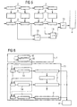
- FIG. 1 schematically shows the structure of a digital module according to a first embodiment of the present invention shown.
- this first embodiment comprises the digital module a test unit 3 with functional elements, a test pattern output register 2 and an evaluation unit 16.
- a self-test unit 1 is provided, in a self-test phase of the digital module the controls necessary functions for self-test.
- the test pattern output register 2 is a shift register with parallel Output and serial input, with the parallel output of the test pattern output register 2, numerous output lines includes, each act on an input of the test unit 3.
- the serial input of the test pattern output register 2 is connected to the self-test unit 1 for this one Test pattern in the form of a digital value, in particular a binary value, serially load into the test pattern output register 2 can.
- the outputs on the right side of the Test unit 3 are connected to inputs of the evaluation unit 16.
- the components of the test pattern output register 2 and / or the evaluation unit 16 and / or the self-test unit 1 can be functional elements of the digital module, outside the self-test phase to normal operation of the Digital modules are used and in the self-test phase be switched to the test pattern output register 2 or the evaluation unit 16 or the self-test unit 1 form.
- Within the test unit 3 are numerous functional elements interconnected, the inputs of the Test unit 3 externally addressable inputs of the functional elements the test unit 3 correspond and the outputs the test unit 3 externally observable outputs of the functional elements the test unit 3 correspond.
- the functional elements within the test unit 3, gates or Be switching elements.
- the test pattern is used the inputs of the test unit 3 from one or more sub-patterns formed, the length or lengths thereof in particular not the maximum or average number of hits for the Outputs of the test unit 3 exceed.
- the individual locations of the subpattern or subpatterns at the outputs of the test pattern output register 2 in FIG whose sliding direction can be next to each other can in this way with the shortest possible sub-patterns a complete Loading the cone 5 can be achieved.
- the digital module can also other test units 3, which each have a test pattern output register 2 and an evaluation unit 16 are assigned, each are connected to the self-test unit 1.
- test patterns For testing the functional elements within the test unit 3 within the self-test unit 1 changing test patterns whose length is the number of inputs of the test unit 3 corresponds to the one after the other in the test pattern output register 2 are loaded.
- the test patterns are starting generated by sub-patterns using a test pattern either partially or completely a periodic sequence of a particular Subpatters may be or a sequence of different Subpattern can be. This essentially depends on it from, in which clock the evaluation unit 16 at the outputs the test unit 3 can evaluate existing test response.
- the evaluation unit 16 at each shift clock of the test pattern output register 2 in which a modified admission of the inputs of Test unit 3 can be achieved and therefore also a set changed test pattern response at the outputs can evaluate the test pattern response.
- the different sub-patterns one after the other into the test pattern output register 2 to load serially, so that the different subpatterns successively at the entrances the impact cone 5 wander past, these sliding operations continue until the last subpattern completely pushed through the test pattern output register 2 has been.
- the various resulting test responses are lossy from the evaluation unit 16 to a Compressed signature, which is a digital value.
- This signature is from the evaluation unit 16 in particular to the serial Self-test unit 1 transfer, so this depending the data loaded into the test pattern output register 2 can determine whether the resulting signature on a proper Function of the functional elements within the Close test unit 3. It is for the selected Sequence of sub-patterns for loading the test unit 3 preferably in advance by the compression by a certain evaluation unit 16 resulting signature when properly Function of the test unit 3 and determined in the Self-test unit 1 filed. This then only needs the from the evaluation unit 16 supplied signature with the filed Compare target signature and so on match determine the proper condition of the test unit 3. In this type of evaluation within the evaluation unit 16, the signature formation is clock-controlled therein, wherein the Clock for signature formation within the evaluation unit 16 with matches the shift clock for the test pattern output register 2.
- each shift clock of the test pattern output register 2 several clocks for signature formation within the evaluation unit 16. Unfortunately, this slows down the bump test of the digital module.
- the evaluation unit 16 may u.U. also be set up so that they themselves already won Check the signature or the read-in test responses to this effect can see if the functional elements within the test unit 3 work correctly.
- test pattern output register 2 completely load with a new test pattern.
- every new test pattern is a periodic consequence of a formed certain sub-pattern.
- test patterns are from the self-test unit 1 sequentially loaded into the test pattern output register 2, wherein the evaluation unit 16, the resulting test response takes over and the self-test unit 1 transmits as soon as the Test pattern output register 2 is loaded with a test pattern.
- the compression of the test response happens in this case in the self-test unit 1.
- the subpatterns may be different in the preceding cases Wise ways are generated.
- a memory for storing the ones to be used Subpattern be present.
- the Self-test unit 1 include a digital counter whose Counter readings are used as sub-patterns. This method can be carried out with very little effort and is particularly suitable for short sub-patterns in which all combinations of individual bodies are used should.
- FIG. 2 shows a digital module according to a second exemplary embodiment of the present invention.
- this 1 again denotes the self-test unit.
- the ones to be tested Components of the digital module are in a functional element block 11 summarized.
- Within the functional element block 11 is an example of a test pattern output register 2 for applying a not shown Test unit 3.
- the functional element block 11 comprises an evaluation unit, not shown, for evaluating the Test answers.
- the interaction between the test pattern output register 2, the test unit and the evaluation unit can in the ways described in the first embodiment respectively.
- the sub-pattern shift register becomes 15 loaded with a sub-pattern and with the multiplexer 18 set a periodicity that is the length of the subpattern equivalent.
- the sub-pattern shift register 15 continues to operate in the sliding direction, the previously charged Sub-pattern repeated as often as desired due to the feedback.
- the thus obtained periodic sequence of the subpattern into the Test pattern output register 2 loaded.
- a memory 6 serving within the self-test unit may serve 1 is arranged.
- a Submustereingangstechnisch 17 provided, which together with the output of the memory 6 leads to a multiplexer 7, with the for applying the sub-pattern shift register 15 either a derived from the memory 6 sub-pattern or from the outside via the Submustereingangs effet 17 supplied sub-pattern can be forwarded.
- a fed back Shift registers are used to subpattern to generate, wherein the input of the shift register with the Result of an exclusive-OR operation between the output and a further shift member of the shift register acted upon and the state of the shift register as a sub-pattern transferred in parallel or serially to the sub-pattern shift register 15 becomes.
- a counter 10 is provided which is the one at the output of the sub-pattern shift register 15 bits pushed out counts.
- the self-test unit 1 has a test control block 8 on, put the functional element block 11 in the test mode can. In this putting in the test mode can For example, certain functional elements within the Function element block 11 to a test pattern output register 2 or switched to an evaluation unit, wherein additionally made the necessary connections for self-test can be.
- test answer acceptance block 9 provided the assumption of a test response in an evaluation unit controls, provided that the evaluation unit used requires such takeover control.
- the self-test of the digital module is carried out as follows. First, the self-test unit 1 of the functional element block 11 by means of the test control block 8 in the test mode added. After selecting the desired source for the one used Sub-pattern by means of the multiplexer 7 is either via the submode input line 17 or from the memory 6 a sub-pattern is loaded into the sub-pattern shift register 15. Dependent of the length of the sub-pattern used is by means of of the multiplexer 18 set the required periodicity. The sub-pattern shift register 15 then becomes long continue to operate in push mode until the test pattern output register 2 complete with a periodic sequence of the subpattern is filled. This is done with the help of the counter 10 monitored.
- test response acceptance block 9 a suitable control command to the functional element block 11, in which at least one Test response is taken in an evaluation.
- the evaluation the test response can be either by means of a suitable designed evaluation within the functional element block 11 take place or carried out outside become.
- a connection, not shown, between the functional element block 11 and the self-test unit 1 is provided be about which the at least one test answer in the Self-test unit 1 are transmitted for local evaluation can.
- at least one Test response either directly or via the self-test unit 1 from outside the digital module and evaluate there. The latter is particularly useful in cases in which the sub-pattern used via the Submustereingangs effet 17 has been supplied from the outside.
- FIG. 3 shows a third embodiment of the present invention Invention, in which a total of three test units 3 and three test pattern output registers 2 are provided.
- the test pattern output registers 2 are in this embodiment designed as a shift register and set up such that they each have a serial output, a serial Input, a parallel output and a parallel input exhibit.
- the parallel inputs of the test pattern output registers 2 are each with an output of a test unit 3 so that the test responses of the test units 3 in FIG the test pattern output register 2 can be adopted.
- the parallel outputs of the test pattern output registers 2 are like previously described with the inputs of the test units 3 to Exposure to a test pattern.
- the serial Inputs are as previously described with the self-test unit 1 connected and the serial outputs with a Evaluation unit 4 connected.
- Each test pattern output register 2 is both energized the inputs of a test unit 3 in a test pattern as also used to take over the test response. Since, however, at Apply the test responses to the test pattern output registers 2 overwrite the content previously contained in it, it is advantageous in this embodiment, first the test pattern output register 2 completely with a new one Load test pattern and then the resulting Test responses by suitable control of the test pattern output registers 2 in it. The into the test pattern output registers 2 loaded test patterns are advantageously same, but may be different.
- Test responses of the test units 3 are in the Sliding operation operated, so that the test answers serially be transmitted to the evaluation unit 4.
- the evaluation unit 4 is operated so that with each shift clock the Test pattern output register 2, with which the test answers in the Evaluation unit 4 are transmitted, the test unit 4 the newly inserted bit compresses.
- FIG. 4 shows a possible structure of the evaluation unit 4 shown.
- the evaluation unit 4 is shown by a feedback shift register of several individual Slide members 12 and 12 individual registers formed.
- the Sliding direction is in the case shown from left to right.
- the input of the first single register 12, the left is shown, is the result of a first exclusive-OR operation between the outputs of the last and of the penultimate single register 12.
- This first Exclusive-OR linking is done with the help of an exclusive OR gate 13, whose two inputs are connected to the output the last or the penultimate single register 12 connected are.
- exclusive-OR gates 13 are provided which between two consecutive individual registers 12 interposed are, wherein they are connected such that the input of a single register 12 resulting in a second exclusive OR connection between the output of preceding single register 12 and one via an input line 19 signal supplied to the evaluated Signal corresponds, is applied.
- the input lines 19 for example, directly the outputs of a test unit be connected or the serial output of a Shift register into which the test response has been taken is and from the test answer serial to the evaluation unit is forwarded.
- the evaluation unit 4 can in the in FIG 4 illustrated form, for example, in the digital module be used according to the third embodiment, wherein for the evaluation unit as many input lines 19 must be provided, such as test pattern output register 2 available are.
- each Output of the test unit 3 with an input line 19 of Evaluation unit 4 must be connected.
- the in Figure 4 shown evaluation must be ensured be that after a change to the input line 19 applied signals at least one shift clock the Single register 12 is performed.
- the individual register 12 at least be switched on a clock.
- the evaluation unit 4 in a digital example according to the first embodiment must also the individual register 12 of the Evaluation unit at each shift cycle of the test pattern output register 2 be advanced by at least one clock.
- FIG. 5 shows a digital module according to a fourth exemplary embodiment of the present invention partially shown.
- the essential difference to the other embodiments is that the test answers faster can be evaluated.
- the test answers faster can be evaluated.
- As in the previous embodiments become test units 3 by means of partial registers 2 subjected to test patterns.
- the for four test units 3 provided four partial registers 2 serially connected to each other so that they have a single large shift register form.
- Apply to the outputs of the four test units 3 four sub-registers 2 set up in this way are that they each have a parallel input the Test response of a test unit 3 can take over.
- the each other associated sub-registers 2 in this case together a single shift register.
- the below shown Partial registers 2 have not shown parallel outputs for applying further test units 3.
- Farther Exclusive-OR gate 13 are provided, which together with the Partial registers 2 are so interconnected that the output of each Partial register with a first input of an Exclusive-OR gate 13 is connected, the second input to the output is connected to that exclusive-OR gate 13, whose first input from the output of the previous partial register 2 is applied.
- FIG. 6 shows a digital module according to a fifth exemplary embodiment of the present invention.
- the essential Features are located in the functional element block 11, in which a plurality of test pattern output registers 2 are provided are also used to record test responses.
- Left of each test pattern output register 2 is a feedback shift register 14 connected, with all feedback shift registers 14 by means of multiplexers 7 together a shift register are interconnected.
- Each multiplexer 7 is set up to receive the input of a feedback shift register 14 either with the output of the feedback Shift register 14 or with the output of a previous one Feedback shift register 14 can connect.
- the multiplexer Figure 7 shows the input either with the output of the feedback shift register 14 or with a sub-pattern output of Connect self-test unit 1.
- the self-test unit 1 comprises a sub-pattern shift register 15 and a memory 6 to record a number of submasters.
- the sub-pattern shift register 15 transmits a sub-pattern serially in the functional element block 11th
- test pattern output registers 2 are inputs an evaluation unit 4 connected, as before described a signature for the evaluation of the test answers all serially pushed out of the test pattern output registers 2 Generate test responses.
- the Multiplexer 7 is driven so that it the inputs of the feedback shift registers 14 with the entrance of the previous one Feedback shift register 14 or the sub-pattern shift register 15 connect.
- This phase becomes a subpattern from the memory 6 by means of the sub-pattern shift register 15 through the first multiplexer 7 in the first feedback shift register 14 loaded. After that it can be repeated either the same subpattern or another subpattern be pushed behind with the result that in the end all Feedback shift register 14 filled with a sub-pattern where the feedback shift registers 14 are dependent on the sub-pattern shifted out from the sub-pattern shift register 15 be filled with any and various sub-patterns can.
- the self-test unit 1 can still do many other not shown Components used to conduct the self-test of the Digital modules are required and related to Other embodiments are described.
Landscapes
- Engineering & Computer Science (AREA)
- General Engineering & Computer Science (AREA)
- Physics & Mathematics (AREA)
- General Physics & Mathematics (AREA)
- Tests Of Electronic Circuits (AREA)
- Test And Diagnosis Of Digital Computers (AREA)
Claims (38)
- Module numérique comprenant des éléments fonctionnels, qui sont associés à au moins une unité de test (3) avec des entrées et des sorties, au moins un registre de sortie de modèle test (2) avec une sortie parallèle pour l'alimentation des entrées de la au moins une unité de test (3) avec un modèle test, et une unité d'autotest (1) pour la commande du registre de sortie de modèle test (2) et pour le chargement du registre de sortie de modèle test (2) avec un modèle test qui présente la forme d'une valeur numérique,
caractérisé en ce que
l'unité d'autotest (1) est aménagée de telle sorte qu'elle génère le modèle test comme une séquence périodique d'un sous-modèle, qui présente également la forme d'une valeur numérique,
une périodicité maximale du modèle test étant calculée en fonction d'au moins un nombre actif d'entrées de l'unité de test (3) pour une sortie déterminée de l'unité de test (3), le nombre actif étant le nombre d'entrées de l'unité de test (3) sur lesquelles uniquement des modifications peuvent avoir des effets sur la sortie déterminée de l'unité de test (3). - Module numérique selon la revendication 1,
caractérisé en ce que
le module numérique présente au moins une unité d'analyse (4) pour l'analyse d'une réponse de modèle test s'appliquant sur les sorties de la au moins une unité de test (3). - Module numérique selon la revendication 2,
caractérisé en ce que
le module numérique présente au moins un registre de lecture de réponse de test qui est relié aux sorties de l'unité de test (3) et est aménagé de telle sorte qu'il peut prendre en charge une réponse de test s'appliquant sur les sorties de l'unité de test (3), au moins dans un mode test du module numérique, et peut la transmettre en série à l'unité d'analyse (4). - Module numérique selon la revendication 3,
caractérisé en ce que
le module numérique présente des éléments fonctionnels qui sont des registres et sont aménagés de telle sorte qu'ils peuvent être commutés de l'unité d'autatest (1) à au moins un registre de lecture de réponse de test (2). - Module numérique selon la revendication 3 ou 4,
caractérisé en ce que
l'unité d'autotest (1) est aménagée de telle sorte qu'elle peut charger les registres de sortie de modèle test (2) complètement avec un nouveau modèle test et activer ensuite les registres de lecture de réponse de test de telle sorte qu'ils prennent en charge la réponse de test. - Module numérique selon l'une quelconque des revendications 3 à 5,
caractérisé en ce que
le registre de lecture de réponse de test est formé par un registre de sortie de modèle test (2) qui présente des entrées qui sont reliées aux sorties d'une unité de test (3). - Module numérique selon l'une des revendications 3 à 6,
caractérisé en ce que
le registre de lecture de réponse de test est un registre de décalage subdivisé en registres de décalage individuels (12) et est aménagé de telle sorte qu'il peut transmettre en série à l'unité d'analyse (4) le résultat d'un enchaínement OU exclusif entre un signal de sortie du dernier, dans le sens de glissement du registre de décalage, registre de décalage individuel (12) et un signal de sortie d'au moins un autre registre de décalage individuel (12). - Module numérique selon l'une des revendications 2 à 7,
caractérisé en ce que
l'unité d'analyse (4) est un registre de décalage à réaction constitué de plusieurs registres individuels (12), dont l'entrée peut être alimentée avec le résultat d'un premier enchaínement OU exclusif entre la sortie du dernier, dans le sens de décalage du registre de décalage, registre individuel (12) et la sortie d'au moins un autre registre individuel (12), l'entrée d'au moins un registre individuel (12) pouvant être alimentée avec le résultat d'au moins un second enchaínement OU exclusif entre le résultat du premier enchaínement OU exclusif ou la sortie du registre individuel (12) précédent et un signal de sortie de la au moins une unité de test (3), l'entrée pouvant être alimentée, dans le cas du premier, dans le sens de décalage, registre individuel (12), avec le résultat d'un autre enchaínement OU exclusif entre le résultat du premier enchaínement OU exclusif et un signal de sortie de la au moins une unité de test (3). - Module numérique selon l'une quelconque des revendications précédentes,
caractérisé en ce que
le registre de sortie de modèle test (2) est un registre de décalage qui est aménagé de telle sorte que le modèle test peut être chargé par l'unité d'autotest (1) en série dans le registre de sortie de modèle test (2). - Module numérique selon l'une quelconque des revendications précédentes,
caractérisé en ce que
le module numérique présente des éléments fonctionnels qui sont des registres et sont aménagés de telle sorte qu'ils peuvent être commutés par l'unité d'autotest (1) à au moins un registre de sortie de modèle test (2). - Module numérique selon l'une quelconque des revendications précédentes,
caractérisé en ce que
l'unité d'autotest (1) présente une mémoire (6) et est aménagée de telle sorte qu'elle peut former le modèle test au moyen d'un sous-modèle déposé dans la mémoire (6) comme séquence périodique du sous-modèle avec une périodicité variable. - Module numérique selon l'une quelconque des revendications précédentes,
caractérisé en ce que
l'unité d'autotest (1) présente un compteur et est aménagée de telle sorte qu'elle peut exploiter le compteur dans le sens de comptage ascendant et/ou descendant et peut former le modèle test au moyen de l'indication du compteur comme sous-modèle. - Module numérique selon l'une quelconque des revendications précédentes,
caractérisé en ce que
le module numérique présente plusieurs registres de sortie de modèle test (2) et est aménagé de telle sorte que les registres de sortie de modèle test (2) sont chargés simultanément avec le même modèle test. - Module numérique selon l'une quelconque des revendications précédentes,
caractérisé en ce que
le module numérique présente au moins un registre de décalage de sous-modèle (14) à réaction, qui peut être chargé avec un sous-modèle et est aménagé de telle sorte qu'il peut sortir en série le modèle test comme séquence périodique du sous-modèle. - Module numérique selon la revendication 14,
caractérisé en ce que
le registre de décalage de sous-modèle (14) est aménagé de telle sorte qu'il peut sortir avec une périodicité variable le modèle test comme séquence périodique du sous-modèle. - Module numérique selon la revendication 14 ou 15,
caractérisé en ce que
le registre de décalage de sous-modèle (14) est contenu dans l'unité d'autotest (1). - Module numérique selon la revendication 14 ou 15,
caractérisé en ce que
les registres du registre de sortie de modèle test (2) peuvent être commutés au moins en partie vers le registre de décalage de sous-modèle (14). - Module numérique selon la revendication 14 ou 15,
caractérisé en ce que
une partie du registre de sortie de modèle test (2) forme le registre de décalage de sous-modèle (14). - Module numérique selon l'une quelconque des revendications précédentes,
caractérisé en ce que
le registre de sortie de modèle test (2) est câblé avec l'unité de test (3) de telle sorte que les entrées de l'unité de test (3), sur lesquelles seules des modifications ont des effets sur une sortie déterminée de l'unité de test (3), sont situées ensemble le plus près possible par rapport à l'ordre de succession des sorties du registre de sortie de modèle test (2). - Module numérique selon l'une ou quelconque des revendications précédentes,
caractérisé en ce que
l'unité de test (3) est aménagée de telle sorte que les nombres actifs d'entrées de l'unité de test (3) pour les sorties de l'unité de test (3) sont les plus petits possibles. - Module numérique selon l'une quelconque des revendications précédentes,
caractérisé en ce que
le module numérique présente des lignes de commande guidées vers l'extérieur pour l'unité d'autotest (1), l'unité d'autotest (1) étant aménagée de telle sorte qu'elle peut être commandée à l'aide d'instructions pouvant être entrées par les lignes de commande. - Module numérique comprenant des éléments fonctionnels, qui sont associés à au moins une unité de test (3) avec des entrées et des sorties, au moins un registre de sortie de modèle test (2) avec une sortie parallèle pour l'alimentation des entrées de la au moins une unité de test (3) avec un modèle test, au moins une unité d'analyse (4) pour l'analyse d'une réponse de modèle test s'appliquant sur les sorties de la au moins une unité de test (3) et une unité d'autotest (1) pour la commande du au moins un registre de sortie de modèle test (2) et de l'unité d'analyse (4) et pour le chargement du registre de sortie de modèle test avec le modèle test qui représente la forme d'une valeur binaire,
caractérisé en ce que
l'unité d'autotest (1) est aménagée de telle sorte qu'elle génère le modèle test comme conséquence d'au moins un sous-modèle pouvant être sélectionné dans une liste de sous-modèles, le registre de sortie de modèle test (2) étant un registre de décalage, qui peut être chargé en série avec le modèle test, et l'unité d'analyse (4) étant aménagée de telle sorte qu'elle peut analyser la réponse de modèle test lors de chaque cycle avec lequel une nouvelle partie de modèle test est chargée dans le registre de sortie de modèle test (2),
la longueur maximale des sous-modèles étant fonction d'au moins un nombre actif d'entrées d'une unité de test (3) pour une sortie déterminée de l'unité de test (3), le nombre actif étant le nombre d'entrées de l'unité de test (3) sur lesquelles uniquement des modifications ont des conséquences sur la sortie déterminée de l'unité de test (3). - Module numérique selon revendication 22,
caractérisé en ce que
l'unité d'analyse (4) est un registre de décalage à réaction constitué de plusieurs registres individuels (12), dont l'entrée est alimentée avec le résultat d'un premier enchaínement OU exclusif entre la sortie du dernier, dans le sens du registre de décalage, registre individuel (12) et la sortie d'au moins un autre registre individuel (12) du registre de décalage. - Module numérique selon revendications 22 ou 23,
caractérisé en ce que
le module numérique présente des éléments fonctionnels qui sont des registres et sont aménagés de telle sorte qu'ils peuvent être commutés de l'unité d'autotest (1) vers le au moins un registre de sortie de modèle test (2). - Module numérique selon l'une ou quelconque des revendications 22 à 24,
caractérisé en ce que
l'unité d'autotest (1) présente une mémoire (6) et est aménagée de telle sorte qu'elle peut former le modèle test au moyen de sous-modèles déposés dans la mémoire (6). - Module numérique selon l'une quelconque des revendications 22 à 25,
caractérisé en ce que
l'unité d'autotest (1) présente un compteur et est aménagée de telle sorte qu'elle peut exploiter le compteur dans un sens de comptage ascendant et/ou descendant et peut former le modèle test au moyen des indications de compteur. - Module numérique selon l'une ou quelconque des revendications 22 à 26,
caractérisé en ce que
le module numérique présente plusieurs registres de sortie de modèle test (2) et est aménagé de telle sorte que les registres de sortie de modèle test (2) sont chargés simultanément avec le même modèle test. - Procédé pour tester un module numérique, le composant numérique présentant des éléments fonctionnels qui sont associés à au moins une unité de test (3) avec des entrées et des sorties, au moins un registre de sortie de modèle test (2) avec une sortie parallèle pour l'alimentation des entrées de la au moins une unité de test (3) avec un modèle test et une unité d'autotest (1) pour la commande du registre de sortie de modèle test (2) et pour le chargement du registre de sortie de modèle test (2) avec un modèle test qui présente la forme d'une valeur numérique,
caractérisé en ce que
le modèle test est généré comme séquence périodique d'un sous-modèle qui représente également la forme d'une valeur numérique,
en ce que le au moins un registre de sortie de modèle test (2) est chargé avec un modèle test, et en ce que le comportement à la réponse de la au moins une unité de test (3) est analysé sur le modèle test,
une périodicité maximale du modèle test étant déterminée en fonction d'au moins un nombre actif d'entrées de l'unité de test (3) pour une sortie déterminée de l'unité de test (3), le nombre actif étant le nombre d'entrées de l'unité de test (3), sur lesquelles uniquement des modifications ont des effets sur la sortie déterminée de l'unité de test (3). - Procédé pour tester un module numérique, le module numérique présentant des éléments fonctionnels qui sont associés à au moins une unité de test (3) avec des entrées et des sorties, et au moins un registre de sortie de modèle test (2) avec une sortie parallèle pour l'alimentation des entrées de la au moins une unité de test (3) avec un modèle test qui présente la forme d'une valeur numérique, le registre de sortie de modèle test (2) étant conçu comme un registre de décalage,
caractérisé en ce que
le registre de sortie de modèle test (2) est chargé en série avec le modèle test, et avec chaque cycle, avec lequel un bit du modèle test est chargé dans le registre de sortie de modèle test (2), on analyse une réponse de modèle test s'appliquant sur les sorties de la au moins une unité de test (3), le modèle test étant généré comme une conséquence d'au moins un sous-modèle pouvant être sélectionné à partir d'une liste de sous-modèles, la longueur maximale de sous-modèles étant fonction d'au moins un nombre actif d'entrées d'une unité de test (3) pour une sortie déterminée de l'unité de test (3), le nombre actif étant le nombre d'entrées de l'unité de test (3) sur lesquelles uniquement des modifications ont des effets sur la sortie déterminée de l'unité de test (3). - Procédé selon la revendication 28 ou 29,
caractérisé en ce que
pour l'analyse d'une réponse de modèle test dans un registre de décalage à réaction avec plusieurs registres individuels (12), son entrée est alimentée avec le résultat d'un premier enchaínement OU exclusif entre la sortie du dernier, dans le sens de glissement, registre individuel (12) et la sortie d'au moins un autre registre individuel (12) du registre de décalage, l'entrée d'au moins un registre individuel (12) étant alimentée avec le résultat d'au moins un second enchaínement OU exclusif entre le résultat du premier enchaínement OU exclusif ou la sortie de registre individuel (12) précédent et un signal de sortie de l'unité de test (3), l'entrée étant alimentée, dans le cas du premier, dans le sens de glissement, registre individuel (12), avec le résultat d'un autre enchaínement OU exclusif entre le résultat du premier enchaínement OU exclusif et un signal de sortie de l'unité de test (3), de sorte qu'une signature est formée dans le registre de décalage à réaction en fonction de la au moins une sortie de l'unité de test (3). - Procédé selon la revendication 28 ou 29,
caractérisé en ce que
une réponse de modèle test s'appliquant sur les sorties de la au moins une unité de test (3) est prise en charge à l'aide d'au moins un registre de lecture de modèle test à un moment défini et transmis en série pour l'analyse à une unité d'analyse (4). - Procédé selon la revendication 31,
caractérisé en ce que
le registre de décalage de modèle test (2) est formé par un registre de sortie de modèle test (2), le contenu du registre de sortie de modèle test (2) étant écrasé lors de la prise en charge de la réponse de modèle test dans un registre de lecture de réponse de modèle test - Procédé selon la revendication 32,
caractérisé en ce que
chaque registre de sortie de modèle test (2) du modèle numérique sert aussi bien à l'alimentation des entrées de la au moins une unité de test (3) avec un modèle test que comme registre de lecture de réponse de modèle test. - Procédé selon la revendication 29 ou 30 et l'une quelconque des revendications 31 à 33,
caractérisé en ce que
la réponse de modèle test de l'unité de test (3) est transmise en série au moyen du registre de lecture de modèle test (2) pour la formation de signature au registre de décalage à réaction pour l'analyse, le cycle de sortie série du registre de lecture de modèle test (2) étant identique au cycle de glissement série du registre de décalage à réaction pour l'analyse. - Procédé selon la revendication 28 ou 29,
caractérisé en ce que
le comportement à la réponse du modèle test de la au moins une unité de test (3) est analysé par le procédé de test à faisceau électronique. - Dispositif pour tester un module numérique, le modèle numérique présentant des éléments fonctionnels, qui sont associés à au moins une unité de test (3) avec des entrées et des sorties, au moins un registre de sortie de modèle test (2) avec une sortie parallèle pour l'alimentation des entrées de la au moins une unité de test (3) avec un modèle test, au moins une unité de lecture ou d'analyse pour la lecture ou pour l'analyse d'une réponse de modèle test s'appliquant sur les sorties de la au moins une unité de test (3), et une unité d'autotest (1) pour la commande du registre de sortie de modèle test (2) et de l'unité d'analyse ou de lecture et pour le chargement du registre de sortie de modèle test (2) avec au moins un modèle test qui présente la forme d'une valeur numérique,
le dispositif présentant un appareil de traitement de données pour la génération de données test et une unité de transmission de modèle test qui est aménagée de telle sorte qu'elle peut transmettre des modèles test dans le module numérique pour le chargement dans le au moins un registre de sortie de modèle test (2),
caractérisé en ce que
le modèle test est une séquence d'au moins un sous-modèle qui peut être sélectionné dans une liste de sous-modèles ou est une conséquence périodique d'un sous-modèle, le sous-modèle présentant également la forme d'une valeur numérique, et le dispositif étant aménagé de telle sorte que l'appareil de traitement de données génère comme données de modèle test le au moins un sous-modèle et le transmet à l'unité de transmission de modèle test et l'unité de transmission de modèle test génère à partir du au moins un sous-modèle reçu de l'unité de traitement de données le modèle test pour le chargement dans le module numérique,
une périodicité maximale du modèle test ou une longueur maximale du sous-modèle étant déterminée en fonction d'au moins un nombre actif d'entrées de l'unité test (3) pour une sortie déterminée de l'unité de test (3), le nombre actif étant le nombre d'entrées de l'unité de test (3), sur lesquelles uniquement des modifications ont des conséquences sur une sortie déterminée de l'unité de test (3). - Dispositif selon la revendication 36,
caractérisé en ce que
l'unité de transmission de modèle test est une plaque à aiguille avec des points de contact pour le contact des points de contact sur le module numérique. - Dispositif pour tester un module numérique selon la revendication 36,
caractérisé en ce que
le dispositif est aménagé de telle sorte qu'il peut transmettre par des lignes de commande sortant du module numérique à l'unité d'autotest (1) à l'intérieur du module numérique des instructions de commande pour générer le au moins un sous-modèle ou des instructions de commande pour la sélection du au moins un sous-modèle à partir de sous-modèles mémorisés ou le au moins un sous-modèle à chaque fois pour générer des modèles test à l'intérieur du module numérique.
Applications Claiming Priority (3)
| Application Number | Priority Date | Filing Date | Title |
|---|---|---|---|
| DE10221611A DE10221611B4 (de) | 2002-05-15 | 2002-05-15 | Digitalbaustein mit einer Selbsttestfunktion |
| DE10221611 | 2002-05-15 | ||
| PCT/EP2003/005058 WO2003098243A1 (fr) | 2002-05-15 | 2003-05-14 | Systeme pour tester des modules numeriques |
Publications (2)
| Publication Number | Publication Date |
|---|---|
| EP1504273A1 EP1504273A1 (fr) | 2005-02-09 |
| EP1504273B1 true EP1504273B1 (fr) | 2005-10-12 |
Family
ID=29413847
Family Applications (1)
| Application Number | Title | Priority Date | Filing Date |
|---|---|---|---|
| EP03720566A Expired - Fee Related EP1504273B1 (fr) | 2002-05-15 | 2003-05-14 | Systeme pour tester des modules numeriques |
Country Status (7)
| Country | Link |
|---|---|
| US (1) | US7386776B2 (fr) |
| EP (1) | EP1504273B1 (fr) |
| JP (1) | JP3892459B2 (fr) |
| CN (1) | CN100526900C (fr) |
| AU (1) | AU2003224158A1 (fr) |
| DE (2) | DE10221611B4 (fr) |
| WO (1) | WO2003098243A1 (fr) |
Families Citing this family (5)
| Publication number | Priority date | Publication date | Assignee | Title |
|---|---|---|---|---|
| DE10221611B4 (de) | 2002-05-15 | 2013-01-24 | Infineon Technologies Ag | Digitalbaustein mit einer Selbsttestfunktion |
| DE102004044813A1 (de) * | 2004-09-16 | 2006-03-23 | Robert Bosch Gmbh | Verfahren zum Testen eines integrierten Schaltkreises |
| US7533314B2 (en) * | 2006-08-10 | 2009-05-12 | Microsoft Corporation | Unit test extender |
| US7941679B2 (en) * | 2007-08-10 | 2011-05-10 | Atrenta, Inc. | Method for computing power savings and determining the preferred clock gating circuit of an integrated circuit design |
| US8868992B2 (en) * | 2009-12-31 | 2014-10-21 | Intel Corporation | Robust memory link testing using memory controller |
Family Cites Families (21)
| Publication number | Priority date | Publication date | Assignee | Title |
|---|---|---|---|---|
| US7137048B2 (en) * | 2001-02-02 | 2006-11-14 | Rambus Inc. | Method and apparatus for evaluating and optimizing a signaling system |
| US5187712A (en) * | 1990-02-26 | 1993-02-16 | At&T Bell Laboratories | Pseudo-exhaustive self-test technique |
| US5278842A (en) * | 1991-02-04 | 1994-01-11 | International Business Machines Corporation | Delay test coverage enhancement for logic circuitry employing level sensitive scan design |
| US5309447A (en) * | 1991-06-03 | 1994-05-03 | At&T Bell Laboratories | Space compression technique for pseudo-exhaustive self-testing of digital electronic circuits |
| JP2584172B2 (ja) * | 1991-08-23 | 1997-02-19 | インターナショナル・ビジネス・マシーンズ・コーポレイション | デイジタル試験信号発生回路 |
| JPH0764817A (ja) * | 1993-08-30 | 1995-03-10 | Mitsubishi Electric Corp | 故障検出システム |
| US5414716A (en) * | 1993-09-22 | 1995-05-09 | Mitsubishi Electronic Research Laboratories, Inc. | Weighting system for testing of circuits utilizing determination of undetected faults |
| US5617531A (en) * | 1993-11-02 | 1997-04-01 | Motorola, Inc. | Data Processor having a built-in internal self test controller for testing a plurality of memories internal to the data processor |
| US6061818A (en) * | 1997-05-08 | 2000-05-09 | The Board Of Trustees Of The Leland Stanford Junior University | Altering bit sequences to contain predetermined patterns |
| US6201829B1 (en) * | 1998-04-03 | 2001-03-13 | Adaptec, Inc. | Serial/parallel GHZ transceiver with pseudo-random built in self test pattern generator |
| US6370664B1 (en) * | 1998-10-29 | 2002-04-09 | Agere Systems Guardian Corp. | Method and apparatus for partitioning long scan chains in scan based BIST architecture |
| US6668347B1 (en) * | 2000-05-08 | 2003-12-23 | Intel Corporation | Built-in self-testing for embedded memory |
| US6782501B2 (en) * | 2001-01-23 | 2004-08-24 | Cadence Design Systems, Inc. | System for reducing test data volume in the testing of logic products |
| US6769084B2 (en) * | 2001-03-13 | 2004-07-27 | Samsung Electronics Co., Ltd. | Built-in self test circuit employing a linear feedback shift register |
| US6782515B2 (en) * | 2002-01-02 | 2004-08-24 | Cadence Design Systems, Inc. | Method for identifying test points to optimize the testing of integrated circuits using a genetic algorithm |
| US6807646B1 (en) * | 2002-03-04 | 2004-10-19 | Synopsys, Inc. | System and method for time slicing deterministic patterns for reseeding in logic built-in self-test |
| JP2003332443A (ja) * | 2002-05-08 | 2003-11-21 | Toshiba Corp | 半導体集積回路とその設計支援装置およびテスト方法 |
| DE10221611B4 (de) | 2002-05-15 | 2013-01-24 | Infineon Technologies Ag | Digitalbaustein mit einer Selbsttestfunktion |
| US7234092B2 (en) * | 2002-06-11 | 2007-06-19 | On-Chip Technologies, Inc. | Variable clocked scan test circuitry and method |
| US6920597B2 (en) * | 2002-07-31 | 2005-07-19 | Thomas Hans Rinderknecht | Uniform testing of tristate nets in logic BIST |
| US20040193986A1 (en) * | 2003-03-31 | 2004-09-30 | Canagasaby Karthisha S. | On-die pattern generator for high speed serial interconnect built-in self test |
-
2002
- 2002-05-15 DE DE10221611A patent/DE10221611B4/de not_active Expired - Fee Related
-
2003
- 2003-05-14 CN CNB038109360A patent/CN100526900C/zh not_active Expired - Fee Related
- 2003-05-14 WO PCT/EP2003/005058 patent/WO2003098243A1/fr active IP Right Grant
- 2003-05-14 EP EP03720566A patent/EP1504273B1/fr not_active Expired - Fee Related
- 2003-05-14 AU AU2003224158A patent/AU2003224158A1/en not_active Abandoned
- 2003-05-14 JP JP2004505712A patent/JP3892459B2/ja not_active Expired - Fee Related
- 2003-05-14 DE DE50301371T patent/DE50301371D1/de not_active Expired - Lifetime
- 2003-05-14 US US10/514,537 patent/US7386776B2/en not_active Expired - Lifetime
Also Published As
| Publication number | Publication date |
|---|---|
| EP1504273A1 (fr) | 2005-02-09 |
| CN100526900C (zh) | 2009-08-12 |
| DE50301371D1 (de) | 2006-02-23 |
| US20060069951A1 (en) | 2006-03-30 |
| JP2006507475A (ja) | 2006-03-02 |
| DE10221611B4 (de) | 2013-01-24 |
| US7386776B2 (en) | 2008-06-10 |
| DE10221611A1 (de) | 2003-12-04 |
| AU2003224158A1 (en) | 2003-12-02 |
| JP3892459B2 (ja) | 2007-03-14 |
| CN1653344A (zh) | 2005-08-10 |
| WO2003098243A1 (fr) | 2003-11-27 |
Similar Documents
| Publication | Publication Date | Title |
|---|---|---|
| DE3130714C2 (fr) | ||
| DE3913219C3 (de) | Integrierte Halbleiterschaltung mit mehreren Schaltungen, die logischen Tests unterworfen werden | |
| DE3627638A1 (de) | Verfahren zum pruefen von traegern mit mehreren digital arbeitenden integrationsschaltungen, mit derartigen schaltungen versehener traeger, geeignete integrationsschaltung zum anbringen auf einem derartigen traeger und pruefanordnung zur pruefung derartiger traeger | |
| EP0009572A2 (fr) | Méthode et dispositif pour le test de circuits séquentiels réalisés en circuits semi-conducteurs qui sont monolithiquement intégrés | |
| EP0903587B1 (fr) | Procédé de test d'un circuit électronique | |
| DE3702408C2 (fr) | ||
| DE3124902C2 (fr) | ||
| DE19536226C2 (de) | Testbare Schaltungsanordnung mit mehreren identischen Schaltungsblöcken | |
| EP0628832B1 (fr) | Circuit intégré comportant des étages de registres | |
| DE102005046588B4 (de) | Vorrichtung und Verfahren zum Test und zur Diagnose digitaler Schaltungen | |
| EP1504273B1 (fr) | Systeme pour tester des modules numeriques | |
| DE10335809B4 (de) | Integrierte Schaltung mit einem zu testenden elektronischen Schaltkreis und Testsystem-Anordnung zum Testen der integrierten Schaltung | |
| DE1424706B2 (de) | Suchvorrichtung zum auffinden von informationen aus ungeordnet zugefuehrten informationsfolgen | |
| DE4017533C2 (fr) | ||
| DE3639577A1 (de) | Logikbaustein zur erzeugung von ungleich verteilten zufallsmustern fuer integrierte schaltungen | |
| DE19651713C2 (de) | Bauelement-Testgerät zum Testen elektronischer Bauelemente | |
| DD145972A5 (de) | Einrichtung zur feststellung der l enge beliebiger schieberegister | |
| DE10338922B4 (de) | Elektrische Diagnoseschaltung sowie Verfahren zum Testen und/oder zur Diagnose einer integrierten Schaltung | |
| EP1178321B1 (fr) | Procédé d'exploitation d'un composant comportant une partie logique et une partie mémoire | |
| EP1179737A2 (fr) | Agencement de test d'un circuit intégré | |
| DE102009000698A1 (de) | Prüfschaltung zur Prüfung einer Durchführung eines Handshake-Protokolls und Verfahren zur Prüfung einer Durchführung eines Handshake-Protokolls | |
| DE19606637A1 (de) | Integrierte Halbleiterschaltungsvorrichtung | |
| DE3911939A1 (de) | Integrierte schaltungsanordnung | |
| DE19604375C2 (de) | Verfahren zur Auswertung von Testantworten zu prüfender digitaler Schaltungen und Schaltungsanordnung zur Durchführung des Verfahrens | |
| DE1549546C3 (de) | Verfahren und Prüfgerät zum Prüfen eines elektronischen Digitalrechners |
Legal Events
| Date | Code | Title | Description |
|---|---|---|---|
| PUAI | Public reference made under article 153(3) epc to a published international application that has entered the european phase |
Free format text: ORIGINAL CODE: 0009012 |
|
| 17P | Request for examination filed |
Effective date: 20041028 |
|
| AK | Designated contracting states |
Kind code of ref document: A1 Designated state(s): AT BE BG CH CY CZ DE DK EE ES FI FR GB GR HU IE IT LI LU MC NL PT RO SE SI SK TR |
|
| AX | Request for extension of the european patent |
Extension state: AL LT LV MK |
|
| GRAP | Despatch of communication of intention to grant a patent |
Free format text: ORIGINAL CODE: EPIDOSNIGR1 |
|
| GRAS | Grant fee paid |
Free format text: ORIGINAL CODE: EPIDOSNIGR3 |
|
| GRAA | (expected) grant |
Free format text: ORIGINAL CODE: 0009210 |
|
| DAX | Request for extension of the european patent (deleted) | ||
| RBV | Designated contracting states (corrected) |
Designated state(s): DE FR GB |
|
| AK | Designated contracting states |
Kind code of ref document: B1 Designated state(s): DE FR GB |
|
| REG | Reference to a national code |
Ref country code: GB Ref legal event code: FG4D Free format text: NOT ENGLISH |
|
| GBT | Gb: translation of ep patent filed (gb section 77(6)(a)/1977) |
Effective date: 20051130 |
|
| REF | Corresponds to: |
Ref document number: 50301371 Country of ref document: DE Date of ref document: 20060223 Kind code of ref document: P |
|
| ET | Fr: translation filed | ||
| PLBE | No opposition filed within time limit |
Free format text: ORIGINAL CODE: 0009261 |
|
| STAA | Information on the status of an ep patent application or granted ep patent |
Free format text: STATUS: NO OPPOSITION FILED WITHIN TIME LIMIT |
|
| 26N | No opposition filed |
Effective date: 20060713 |
|
| PGFP | Annual fee paid to national office [announced via postgrant information from national office to epo] |
Ref country code: DE Payment date: 20150721 Year of fee payment: 13 |
|
| REG | Reference to a national code |
Ref country code: FR Ref legal event code: PLFP Year of fee payment: 14 |
|
| PGFP | Annual fee paid to national office [announced via postgrant information from national office to epo] |
Ref country code: GB Payment date: 20160520 Year of fee payment: 14 |
|
| PGFP | Annual fee paid to national office [announced via postgrant information from national office to epo] |
Ref country code: FR Payment date: 20160520 Year of fee payment: 14 |
|
| REG | Reference to a national code |
Ref country code: DE Ref legal event code: R119 Ref document number: 50301371 Country of ref document: DE |
|
| PG25 | Lapsed in a contracting state [announced via postgrant information from national office to epo] |
Ref country code: DE Free format text: LAPSE BECAUSE OF NON-PAYMENT OF DUE FEES Effective date: 20161201 |
|
| GBPC | Gb: european patent ceased through non-payment of renewal fee |
Effective date: 20170514 |
|
| REG | Reference to a national code |
Ref country code: FR Ref legal event code: ST Effective date: 20180131 |
|
| PG25 | Lapsed in a contracting state [announced via postgrant information from national office to epo] |
Ref country code: GB Free format text: LAPSE BECAUSE OF NON-PAYMENT OF DUE FEES Effective date: 20170514 |
|
| PG25 | Lapsed in a contracting state [announced via postgrant information from national office to epo] |
Ref country code: FR Free format text: LAPSE BECAUSE OF NON-PAYMENT OF DUE FEES Effective date: 20170531 |