EP0902315A2 - Herstellungsverfahren für ein Substrat mit einer Schwarzmatrix und einer Farbfilteranordnung - Google Patents
Herstellungsverfahren für ein Substrat mit einer Schwarzmatrix und einer Farbfilteranordnung Download PDFInfo
- Publication number
- EP0902315A2 EP0902315A2 EP98116679A EP98116679A EP0902315A2 EP 0902315 A2 EP0902315 A2 EP 0902315A2 EP 98116679 A EP98116679 A EP 98116679A EP 98116679 A EP98116679 A EP 98116679A EP 0902315 A2 EP0902315 A2 EP 0902315A2
- Authority
- EP
- European Patent Office
- Prior art keywords
- color filter
- ink
- black matrix
- substrate
- alignment mark
- Prior art date
- Legal status (The legal status is an assumption and is not a legal conclusion. Google has not performed a legal analysis and makes no representation as to the accuracy of the status listed.)
- Granted
Links
- 239000000758 substrate Substances 0.000 title claims abstract description 80
- 238000004519 manufacturing process Methods 0.000 title claims abstract description 27
- 239000011159 matrix material Substances 0.000 title claims description 48
- 238000000034 method Methods 0.000 claims description 42
- 239000004973 liquid crystal related substance Substances 0.000 claims description 39
- 150000001875 compounds Chemical class 0.000 claims description 10
- 239000000463 material Substances 0.000 claims description 7
- 239000000976 ink Substances 0.000 description 57
- 239000010410 layer Substances 0.000 description 33
- LYCAIKOWRPUZTN-UHFFFAOYSA-N Ethylene glycol Chemical compound OCCO LYCAIKOWRPUZTN-UHFFFAOYSA-N 0.000 description 18
- 229920005989 resin Polymers 0.000 description 17
- 239000011347 resin Substances 0.000 description 17
- 238000004040 coloring Methods 0.000 description 11
- 239000011342 resin composition Substances 0.000 description 11
- PEDCQBHIVMGVHV-UHFFFAOYSA-N Glycerine Chemical compound OCC(O)CO PEDCQBHIVMGVHV-UHFFFAOYSA-N 0.000 description 9
- KFZMGEQAYNKOFK-UHFFFAOYSA-N Isopropanol Chemical compound CC(C)O KFZMGEQAYNKOFK-UHFFFAOYSA-N 0.000 description 9
- XLYOFNOQVPJJNP-UHFFFAOYSA-N water Substances O XLYOFNOQVPJJNP-UHFFFAOYSA-N 0.000 description 9
- 229920001187 thermosetting polymer Polymers 0.000 description 8
- 238000010521 absorption reaction Methods 0.000 description 7
- 238000010438 heat treatment Methods 0.000 description 7
- RTZKZFJDLAIYFH-UHFFFAOYSA-N Diethyl ether Chemical compound CCOCC RTZKZFJDLAIYFH-UHFFFAOYSA-N 0.000 description 6
- LFQSCWFLJHTTHZ-UHFFFAOYSA-N Ethanol Chemical compound CCO LFQSCWFLJHTTHZ-UHFFFAOYSA-N 0.000 description 6
- SECXISVLQFMRJM-UHFFFAOYSA-N N-Methylpyrrolidone Chemical compound CN1CCCC1=O SECXISVLQFMRJM-UHFFFAOYSA-N 0.000 description 6
- 239000003086 colorant Substances 0.000 description 6
- 239000000975 dye Substances 0.000 description 6
- 239000011521 glass Substances 0.000 description 6
- 230000003287 optical effect Effects 0.000 description 5
- 239000000049 pigment Substances 0.000 description 5
- 239000011241 protective layer Substances 0.000 description 5
- SMZOUWXMTYCWNB-UHFFFAOYSA-N 2-(2-methoxy-5-methylphenyl)ethanamine Chemical compound COC1=CC=C(C)C=C1CCN SMZOUWXMTYCWNB-UHFFFAOYSA-N 0.000 description 4
- NIXOWILDQLNWCW-UHFFFAOYSA-N 2-Propenoic acid Natural products OC(=O)C=C NIXOWILDQLNWCW-UHFFFAOYSA-N 0.000 description 4
- VVQNEPGJFQJSBK-UHFFFAOYSA-N Methyl methacrylate Chemical compound COC(=O)C(C)=C VVQNEPGJFQJSBK-UHFFFAOYSA-N 0.000 description 4
- 230000015572 biosynthetic process Effects 0.000 description 4
- 238000000576 coating method Methods 0.000 description 4
- 230000007547 defect Effects 0.000 description 4
- 238000004070 electrodeposition Methods 0.000 description 4
- 239000003822 epoxy resin Substances 0.000 description 4
- 238000000206 photolithography Methods 0.000 description 4
- 229920000647 polyepoxide Polymers 0.000 description 4
- 238000004528 spin coating Methods 0.000 description 4
- 238000004544 sputter deposition Methods 0.000 description 4
- KATAXDCYPGGJNJ-UHFFFAOYSA-N 1,3-bis(oxiran-2-ylmethoxy)propan-2-ol Chemical compound C1OC1COCC(O)COCC1CO1 KATAXDCYPGGJNJ-UHFFFAOYSA-N 0.000 description 3
- FGUUSXIOTUKUDN-IBGZPJMESA-N C1(=CC=CC=C1)N1C2=C(NC([C@H](C1)NC=1OC(=NN=1)C1=CC=CC=C1)=O)C=CC=C2 Chemical compound C1(=CC=CC=C1)N1C2=C(NC([C@H](C1)NC=1OC(=NN=1)C1=CC=CC=C1)=O)C=CC=C2 FGUUSXIOTUKUDN-IBGZPJMESA-N 0.000 description 3
- GAWIXWVDTYZWAW-UHFFFAOYSA-N C[CH]O Chemical group C[CH]O GAWIXWVDTYZWAW-UHFFFAOYSA-N 0.000 description 3
- CERQOIWHTDAKMF-UHFFFAOYSA-M Methacrylate Chemical compound CC(=C)C([O-])=O CERQOIWHTDAKMF-UHFFFAOYSA-M 0.000 description 3
- SMNRFWMNPDABKZ-WVALLCKVSA-N [[(2R,3S,4R,5S)-5-(2,6-dioxo-3H-pyridin-3-yl)-3,4-dihydroxyoxolan-2-yl]methoxy-hydroxyphosphoryl] [[[(2R,3S,4S,5R,6R)-4-fluoro-3,5-dihydroxy-6-(hydroxymethyl)oxan-2-yl]oxy-hydroxyphosphoryl]oxy-hydroxyphosphoryl] hydrogen phosphate Chemical compound OC[C@H]1O[C@H](OP(O)(=O)OP(O)(=O)OP(O)(=O)OP(O)(=O)OC[C@H]2O[C@H]([C@H](O)[C@@H]2O)C2C=CC(=O)NC2=O)[C@H](O)[C@@H](F)[C@@H]1O SMNRFWMNPDABKZ-WVALLCKVSA-N 0.000 description 3
- 125000003178 carboxy group Chemical group [H]OC(*)=O 0.000 description 3
- 239000011248 coating agent Substances 0.000 description 3
- 238000001035 drying Methods 0.000 description 3
- 125000002887 hydroxy group Chemical group [H]O* 0.000 description 3
- 238000005342 ion exchange Methods 0.000 description 3
- 239000000203 mixture Substances 0.000 description 3
- 239000003960 organic solvent Substances 0.000 description 3
- 230000036961 partial effect Effects 0.000 description 3
- 229920000642 polymer Polymers 0.000 description 3
- 238000012545 processing Methods 0.000 description 3
- 230000001681 protective effect Effects 0.000 description 3
- 229920001897 terpolymer Polymers 0.000 description 3
- JQNSWTWZESAPPA-UHFFFAOYSA-N 6-amino-5-[[3-[ethyl(phenyl)sulfamoyl]-4-methylphenyl]diazenyl]-4-hydroxynaphthalene-2-sulfonic acid Chemical compound CCN(C1=CC=CC=C1)S(=O)(=O)C1=C(C)C=CC(=C1)N=NC1=C(N)C=CC2=CC(=CC(O)=C12)S(O)(=O)=O JQNSWTWZESAPPA-UHFFFAOYSA-N 0.000 description 2
- VYZAMTAEIAYCRO-UHFFFAOYSA-N Chromium Chemical compound [Cr] VYZAMTAEIAYCRO-UHFFFAOYSA-N 0.000 description 2
- 239000004971 Cross linker Substances 0.000 description 2
- 239000004593 Epoxy Substances 0.000 description 2
- 229920000877 Melamine resin Polymers 0.000 description 2
- 230000005856 abnormality Effects 0.000 description 2
- 239000002585 base Substances 0.000 description 2
- 229910052804 chromium Inorganic materials 0.000 description 2
- 239000011651 chromium Substances 0.000 description 2
- 230000000052 comparative effect Effects 0.000 description 2
- 238000000151 deposition Methods 0.000 description 2
- 230000008021 deposition Effects 0.000 description 2
- 238000010586 diagram Methods 0.000 description 2
- FPAYXBWMYIMERV-UHFFFAOYSA-L disodium;5-methyl-2-[[4-(4-methyl-2-sulfonatoanilino)-9,10-dioxoanthracen-1-yl]amino]benzenesulfonate Chemical compound [Na+].[Na+].[O-]S(=O)(=O)C1=CC(C)=CC=C1NC(C=1C(=O)C2=CC=CC=C2C(=O)C=11)=CC=C1NC1=CC=C(C)C=C1S([O-])(=O)=O FPAYXBWMYIMERV-UHFFFAOYSA-L 0.000 description 2
- XPRMZBUQQMPKCR-UHFFFAOYSA-L disodium;8-anilino-5-[[4-[(3-sulfonatophenyl)diazenyl]naphthalen-1-yl]diazenyl]naphthalene-1-sulfonate Chemical compound [Na+].[Na+].[O-]S(=O)(=O)C1=CC=CC(N=NC=2C3=CC=CC=C3C(N=NC=3C4=CC=CC(=C4C(NC=4C=CC=CC=4)=CC=3)S([O-])(=O)=O)=CC=2)=C1 XPRMZBUQQMPKCR-UHFFFAOYSA-L 0.000 description 2
- 238000004043 dyeing Methods 0.000 description 2
- 238000005192 partition Methods 0.000 description 2
- 238000000059 patterning Methods 0.000 description 2
- 238000007639 printing Methods 0.000 description 2
- 230000002829 reductive effect Effects 0.000 description 2
- 238000007789 sealing Methods 0.000 description 2
- 239000002904 solvent Substances 0.000 description 2
- 229920003051 synthetic elastomer Polymers 0.000 description 2
- 229920002818 (Hydroxyethyl)methacrylate Polymers 0.000 description 1
- FPZWZCWUIYYYBU-UHFFFAOYSA-N 2-(2-ethoxyethoxy)ethyl acetate Chemical compound CCOCCOCCOC(C)=O FPZWZCWUIYYYBU-UHFFFAOYSA-N 0.000 description 1
- ZNQVEEAIQZEUHB-UHFFFAOYSA-N 2-ethoxyethanol Chemical compound CCOCCO ZNQVEEAIQZEUHB-UHFFFAOYSA-N 0.000 description 1
- KXGFMDJXCMQABM-UHFFFAOYSA-N 2-methoxy-6-methylphenol Chemical compound [CH]OC1=CC=CC([CH])=C1O KXGFMDJXCMQABM-UHFFFAOYSA-N 0.000 description 1
- 239000004925 Acrylic resin Substances 0.000 description 1
- 229920000178 Acrylic resin Polymers 0.000 description 1
- WOBHKFSMXKNTIM-UHFFFAOYSA-N Hydroxyethyl methacrylate Chemical compound CC(=C)C(=O)OCCO WOBHKFSMXKNTIM-UHFFFAOYSA-N 0.000 description 1
- 239000004640 Melamine resin Substances 0.000 description 1
- CNCOEDDPFOAUMB-UHFFFAOYSA-N N-Methylolacrylamide Chemical compound OCNC(=O)C=C CNCOEDDPFOAUMB-UHFFFAOYSA-N 0.000 description 1
- 150000008065 acid anhydrides Chemical class 0.000 description 1
- 239000000980 acid dye Substances 0.000 description 1
- 229920006243 acrylic copolymer Polymers 0.000 description 1
- 230000002411 adverse Effects 0.000 description 1
- 239000003513 alkali Substances 0.000 description 1
- 125000003368 amide group Chemical group 0.000 description 1
- 150000001412 amines Chemical class 0.000 description 1
- 239000002518 antifoaming agent Substances 0.000 description 1
- 239000004599 antimicrobial Substances 0.000 description 1
- 150000001732 carboxylic acid derivatives Chemical class 0.000 description 1
- 239000001913 cellulose Substances 0.000 description 1
- 229920002678 cellulose Polymers 0.000 description 1
- 239000003795 chemical substances by application Substances 0.000 description 1
- 238000007796 conventional method Methods 0.000 description 1
- 230000007423 decrease Effects 0.000 description 1
- 238000013461 design Methods 0.000 description 1
- 238000011161 development Methods 0.000 description 1
- 238000007598 dipping method Methods 0.000 description 1
- 239000000982 direct dye Substances 0.000 description 1
- 239000000986 disperse dye Substances 0.000 description 1
- 239000006185 dispersion Substances 0.000 description 1
- 230000000694 effects Effects 0.000 description 1
- 239000003792 electrolyte Substances 0.000 description 1
- 239000005262 ferroelectric liquid crystals (FLCs) Substances 0.000 description 1
- 239000012530 fluid Substances 0.000 description 1
- 239000003999 initiator Substances 0.000 description 1
- 238000005304 joining Methods 0.000 description 1
- 239000007788 liquid Substances 0.000 description 1
- JDSHMPZPIAZGSV-UHFFFAOYSA-N melamine Chemical compound NC1=NC(N)=NC(N)=N1 JDSHMPZPIAZGSV-UHFFFAOYSA-N 0.000 description 1
- 229910052751 metal Inorganic materials 0.000 description 1
- 239000002184 metal Substances 0.000 description 1
- 239000000178 monomer Substances 0.000 description 1
- 229920001568 phenolic resin Polymers 0.000 description 1
- 239000005011 phenolic resin Substances 0.000 description 1
- 229920002120 photoresistant polymer Polymers 0.000 description 1
- 239000004033 plastic Substances 0.000 description 1
- 239000002861 polymer material Substances 0.000 description 1
- 229920005990 polystyrene resin Polymers 0.000 description 1
- 239000000985 reactive dye Substances 0.000 description 1
- 229920003987 resole Polymers 0.000 description 1
- 239000011369 resultant mixture Substances 0.000 description 1
- 230000002441 reversible effect Effects 0.000 description 1
- 238000007761 roller coating Methods 0.000 description 1
- 239000003566 sealing material Substances 0.000 description 1
- 239000011877 solvent mixture Substances 0.000 description 1
- 125000006850 spacer group Chemical group 0.000 description 1
- 238000005507 spraying Methods 0.000 description 1
- 239000004094 surface-active agent Substances 0.000 description 1
- 238000002834 transmittance Methods 0.000 description 1
- -1 triphenylsulfonium hexafluoroantimonate Chemical compound 0.000 description 1
- 229920003169 water-soluble polymer Polymers 0.000 description 1
Images


Classifications
-
- G—PHYSICS
- G02—OPTICS
- G02F—OPTICAL DEVICES OR ARRANGEMENTS FOR THE CONTROL OF LIGHT BY MODIFICATION OF THE OPTICAL PROPERTIES OF THE MEDIA OF THE ELEMENTS INVOLVED THEREIN; NON-LINEAR OPTICS; FREQUENCY-CHANGING OF LIGHT; OPTICAL LOGIC ELEMENTS; OPTICAL ANALOGUE/DIGITAL CONVERTERS
- G02F1/00—Devices or arrangements for the control of the intensity, colour, phase, polarisation or direction of light arriving from an independent light source, e.g. switching, gating or modulating; Non-linear optics
- G02F1/01—Devices or arrangements for the control of the intensity, colour, phase, polarisation or direction of light arriving from an independent light source, e.g. switching, gating or modulating; Non-linear optics for the control of the intensity, phase, polarisation or colour
- G02F1/13—Devices or arrangements for the control of the intensity, colour, phase, polarisation or direction of light arriving from an independent light source, e.g. switching, gating or modulating; Non-linear optics for the control of the intensity, phase, polarisation or colour based on liquid crystals, e.g. single liquid crystal display cells
- G02F1/133—Constructional arrangements; Operation of liquid crystal cells; Circuit arrangements
- G02F1/1333—Constructional arrangements; Manufacturing methods
- G02F1/1335—Structural association of cells with optical devices, e.g. polarisers or reflectors
- G02F1/133509—Filters, e.g. light shielding masks
- G02F1/133514—Colour filters
- G02F1/133516—Methods for their manufacture, e.g. printing, electro-deposition or photolithography
-
- G—PHYSICS
- G02—OPTICS
- G02F—OPTICAL DEVICES OR ARRANGEMENTS FOR THE CONTROL OF LIGHT BY MODIFICATION OF THE OPTICAL PROPERTIES OF THE MEDIA OF THE ELEMENTS INVOLVED THEREIN; NON-LINEAR OPTICS; FREQUENCY-CHANGING OF LIGHT; OPTICAL LOGIC ELEMENTS; OPTICAL ANALOGUE/DIGITAL CONVERTERS
- G02F1/00—Devices or arrangements for the control of the intensity, colour, phase, polarisation or direction of light arriving from an independent light source, e.g. switching, gating or modulating; Non-linear optics
- G02F1/01—Devices or arrangements for the control of the intensity, colour, phase, polarisation or direction of light arriving from an independent light source, e.g. switching, gating or modulating; Non-linear optics for the control of the intensity, phase, polarisation or colour
- G02F1/13—Devices or arrangements for the control of the intensity, colour, phase, polarisation or direction of light arriving from an independent light source, e.g. switching, gating or modulating; Non-linear optics for the control of the intensity, phase, polarisation or colour based on liquid crystals, e.g. single liquid crystal display cells
- G02F1/133—Constructional arrangements; Operation of liquid crystal cells; Circuit arrangements
- G02F1/1333—Constructional arrangements; Manufacturing methods
- G02F1/1335—Structural association of cells with optical devices, e.g. polarisers or reflectors
-
- G—PHYSICS
- G02—OPTICS
- G02B—OPTICAL ELEMENTS, SYSTEMS OR APPARATUS
- G02B5/00—Optical elements other than lenses
- G02B5/20—Filters
- G02B5/201—Filters in the form of arrays
-
- G—PHYSICS
- G02—OPTICS
- G02F—OPTICAL DEVICES OR ARRANGEMENTS FOR THE CONTROL OF LIGHT BY MODIFICATION OF THE OPTICAL PROPERTIES OF THE MEDIA OF THE ELEMENTS INVOLVED THEREIN; NON-LINEAR OPTICS; FREQUENCY-CHANGING OF LIGHT; OPTICAL LOGIC ELEMENTS; OPTICAL ANALOGUE/DIGITAL CONVERTERS
- G02F1/00—Devices or arrangements for the control of the intensity, colour, phase, polarisation or direction of light arriving from an independent light source, e.g. switching, gating or modulating; Non-linear optics
- G02F1/01—Devices or arrangements for the control of the intensity, colour, phase, polarisation or direction of light arriving from an independent light source, e.g. switching, gating or modulating; Non-linear optics for the control of the intensity, phase, polarisation or colour
- G02F1/13—Devices or arrangements for the control of the intensity, colour, phase, polarisation or direction of light arriving from an independent light source, e.g. switching, gating or modulating; Non-linear optics for the control of the intensity, phase, polarisation or colour based on liquid crystals, e.g. single liquid crystal display cells
- G02F1/133—Constructional arrangements; Operation of liquid crystal cells; Circuit arrangements
- G02F1/1333—Constructional arrangements; Manufacturing methods
- G02F1/1335—Structural association of cells with optical devices, e.g. polarisers or reflectors
- G02F1/133509—Filters, e.g. light shielding masks
- G02F1/133512—Light shielding layers, e.g. black matrix
-
- B—PERFORMING OPERATIONS; TRANSPORTING
- B41—PRINTING; LINING MACHINES; TYPEWRITERS; STAMPS
- B41J—TYPEWRITERS; SELECTIVE PRINTING MECHANISMS, i.e. MECHANISMS PRINTING OTHERWISE THAN FROM A FORME; CORRECTION OF TYPOGRAPHICAL ERRORS
- B41J2202/00—Embodiments of or processes related to ink-jet or thermal heads
- B41J2202/01—Embodiments of or processes related to ink-jet heads
- B41J2202/09—Ink jet technology used for manufacturing optical filters
-
- G—PHYSICS
- G02—OPTICS
- G02F—OPTICAL DEVICES OR ARRANGEMENTS FOR THE CONTROL OF LIGHT BY MODIFICATION OF THE OPTICAL PROPERTIES OF THE MEDIA OF THE ELEMENTS INVOLVED THEREIN; NON-LINEAR OPTICS; FREQUENCY-CHANGING OF LIGHT; OPTICAL LOGIC ELEMENTS; OPTICAL ANALOGUE/DIGITAL CONVERTERS
- G02F1/00—Devices or arrangements for the control of the intensity, colour, phase, polarisation or direction of light arriving from an independent light source, e.g. switching, gating or modulating; Non-linear optics
- G02F1/01—Devices or arrangements for the control of the intensity, colour, phase, polarisation or direction of light arriving from an independent light source, e.g. switching, gating or modulating; Non-linear optics for the control of the intensity, phase, polarisation or colour
- G02F1/13—Devices or arrangements for the control of the intensity, colour, phase, polarisation or direction of light arriving from an independent light source, e.g. switching, gating or modulating; Non-linear optics for the control of the intensity, phase, polarisation or colour based on liquid crystals, e.g. single liquid crystal display cells
- G02F1/133—Constructional arrangements; Operation of liquid crystal cells; Circuit arrangements
- G02F1/1333—Constructional arrangements; Manufacturing methods
- G02F1/133354—Arrangements for aligning or assembling substrates
Definitions
- the present invention relates to a color filter substrate manufacturing method and color filter substrate used for color display devices and, more particularly, to a color filter substrate manufacturing method and color filter substrate suitable for color liquid crystal display devices used for color televisions, car televisions, personal computers and the like, and a liquid crystal element using the color filter substrate.
- the first method is a pigment dispersion method.
- a pigment-dispersed photosensitive resin layer is formed on a substrate and patterned into a single-color pattern. This process is repeated three times to obtain R, G, and B color filter layers.
- the second method is a dyeing method.
- a glass substrate is coated with a water-soluble polymer material as a dyeable material, and the coating is patterned into a desired shape by a photolithography process.
- the obtained pattern is dipped in a dye bath to obtain a colored pattern. This process is repeated three times to form R, G, and B color filter layers.
- the third method is an electrodeposition method.
- a transparent electrode is patterned on a substrate, and the resultant structure is dipped in an electrodeposition coating fluid containing a pigment, a resin, an electrolyte, and the like to be colored in the first color by electrodeposition. This process is repeated three times to form R, G, and B color filter layers. Finally, these layers are thermally cured.
- the fourth method is a printing method.
- a pigment is dispersed in a thermosetting resin, and a printing operation is repeated three times to form R, G, and B coatings separately. Colored layers are then formed by thermosetting the resins.
- a protective layer is generally formed on the colored layers.
- the alignment mark formed in a region outside the effective display region is used for drawing alignment by the ink-jet head. Accordingly, the distance between the alignment mark and the nozzle position of the ink-jet head is long, and drawing often shifts.
- the color filter is distorted outside the effective display region, i.e., near the edge of the color filter. A large distortion obstructs proper alignment.
- the alignment mark In order to form the alignment mark, a margin must be ensured outside the effective display region. This reduces the effective display region for displaying an image with respect to the size of the color filter substrate, and thus the substrate cannot be effectively used. Further, when a liquid crystal element is constituted using such a color filter substrate, the positional relationship with the alignment mark of a counter array substrate must be considered. This limitation complicates the design.
- the present invention has been made to solve the above problems, and has as its object to provide a color filter substrate manufacturing method capable of applying a coloring ink with high precision under high-precision alignment and manufacturing a color filter with high reliability without color mixing and color omission, a color filter substrate manufactured by this manufacturing method, and a liquid crystal element.
- a color filter substrate manufacturing method comprising the steps of forming a black matrix on a support substrate, and a forming a color filter by an ink-jet system, wherein an alignment mark is formed within an effective display region, and drawing alignment is performed using the alignment mark in forming the color filter.
- a color filter substrate manufactured by the manufacturing method.
- a liquid crystal element constituted by the color filter substrate.
- an alignment mark is formed in an effective display region and used for alignment in forming a color filter.
- a color filter substrate comprises a substrate 1, a black matrix 2, an alignment mark 3, and opening portions 4 of the black matrix 2.
- Fig. 1B is a schematic sectional view taken along the line 1B - 1B in Fig. 1A.
- a color filter is made up of non-colored portions 5 and colored portions 6, and covered with a protective layer 7, if necessary.
- the color filter and the protective layer on it are not illustrated.
- the side edge section of the black matrix is a frame-like light-shielding region around the effective display region, and the effective display region is a portion surrounded by the side edge section and used to display an image.
- examples of the alignment mark are an alignment mark formed from the same material as the black matrix 2 in the opening portion 4, as shown in Figs. 1A and 1B, and a light-transmitting portion 10 formed in the black matrix 2, as shown in Figs. 9 and 10.
- Other examples of the alignment mark are a light-transmitting portion 11 formed in the black matrix 2, as shown in Fig. 6, a projection 12 formed on the side wall of the opening portion 4, as shown in Fig. 7, a recess 13 formed in the side wall of the opening portion 4, as shown in Fig. 8, and a combination of them.
- the alignment mark is desirably formed in an opening portion 4 at the corner of the effective display region so as not to adversely affect the display of an image.
- the size of the alignment mark is preferably 1/10 to 1/3, and more preferably 1/8 to 1/3 the area of the opening portion 4 where the alignment mark 3 is formed.
- Figs. 2A to 2F show an embodiment of a color filter substrate manufacturing method according to the present invention.
- an alignment mark having a pattern shown in Fig. 1A is formed.
- Figs. 2A to 2F are schematic sectional views corresponding to the following step-a to step-f, respectively.
- a black matrix 2 and an alignment mark 3 are simultaneously formed on a substrate 1 by photolithography.
- a glass substrate is generally used, but may be a plastic substrate as far as the substrate has characteristics, such as the strength, required for the application purpose of the color filter substrate without impairing the transparency of the color filter.
- an opaque substrate may be used as the substrate 1.
- the black matrix 2 is generally obtained by forming a metal film such as a chromium film about 0.1 to 0.5 ⁇ m in thickness by sputtering, deposition, or the like, and patterning the film into a predetermined shape.
- the ink receptive layer 21 is formed on the substrate 1.
- the ink receptive layer 21 is made of an ink absorptive resin composition, e.g., a resin composition which exhibits or loses ink absorption by light irradiation and/or heating.
- the resin composition which exhibits ink absorption by light irradiation and/or heating the ink absorption is attained by exposing the ink receptive layer 21 in advance. It is preferable to use a resin composition which exhibits or loses ink absorption by light irradiation, to form exposed and unexposed portions by pattern exposure in step-c (to be described below), and to selectively color only an ink absorptive region.
- an acrylic resin, an epoxy resin, an amido resin, a phenolic resin, or a polystyrene resin is used together with an optical initiator (crosslinker) if necessary.
- the resin composition is applied on the substrate 1 by, e.g., spin coating, roller coating, bar coating, spray coating, or dipping, and is pre-baked, as needed, to form the ink receptive layer 21.
- the ink receptive layer 21 has a thickness of about 0.4 to 2.0 ⁇ m when a liquid crystal element is to be formed.
- the ink receptive layer 21 is exposed to a pattern using a photomask 22 to form non-colored portions 5 having no ink absorption.
- the ink receptive layer 21 in Figs. 2A to 2F has ink absorption which disappears by exposure. If a resin composition which exhibits ink absorption by exposure is used, the ink receptive layer 21 is exposed to a reverse pattern.
- each non-colored portion 5 is formed on the black matrix 2 to be narrower than the black matrix 2 in order to prevent color omission.
- a predetermined color pattern is drawn by applying R, G, and B coloring inks 24 using an ink-jet head 23 to predetermined positions between the non-colored portions of the ink receptive layer 21.
- the alignment mark 3 is used for drawing alignment of the ink-jet head 23 and the non-colored portions.
- the alignment mark 3 used for drawing alignment is formed in the effective display region of the black matrix 2, the distance from the alignment mark to the drawing position is short, and drawing alignment is almost free from distortion at the edge of the substrate. Therefore, the drawing shift can be minimized, and no margin for forming the alignment mark need be prepared in a region outside the black matrix 2. Since the alignment mark 3 of the present invention is formed at the same time as the black matrix 2, it is not influenced by the positional shift between the substrate 1 and the black matrix 2.
- a bubble-jet type device using an electrothermal converter as an energy generating element a piezoelectric jet type device using a piezoelectric element, or the like can be used.
- a coloring area and coloring pattern can be arbitrarily set.
- the coloring ink 24 used in the present invention is not limited to an ink which contains a dye and is liquified at the room temperature, but may also be an ink which is solidified at room temperature or lower, and an ink which is softened or liquified at room temperature.
- any ink which is liquefied within the above temperature range can be preferably used.
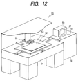
- Fig. 12 is a schematic view showing an example of a color filter manufacturing apparatus using the ink-jet system.
- a manufacturing apparatus 50 comprises an apparatus base 51, an X-Y- ⁇ stage 52 disposed on the apparatus base 51, a support substrate 53 set on the X-Y- ⁇ stage 52, an ink-jet head 55, a controller 58 for controlling the overall operation of this apparatus, a teaching pendant (personal computer) 59 serving as the input/output means of the controller, a keyboard 60 as the operation unit of the teaching pendant 59, and a display 62 for displaying information about the manufacturing progress, the presence/absence of an ink-jet head abnormality, and the like.
- a black matrix and an ink receptive layer are formed on the support substrate 53 but are not illustrated in Fig. 12 for the sake of simplicity.
- Fig. 13 is a block diagram showing the arrangement of the controller 58 of the manufacturing apparatus in Fig. 12.
- the controller 58 comprises an interface 65 for exchanging data between the teaching pendant 59 and the controller 58, a CPU 66 for controlling the color filter manufacturing apparatus 50, a ROM 67 storing control programs for operating the CPU 66, a RAM 68 for storing abnormality information and the like, an ink-jet control unit 70 for controlling application of a coloring ink from the ink-jet head 55 to the support substrate 53, and a stage control unit 71 for controlling the operation of the X-Y- ⁇ stage 52 of the color filter manufacturing apparatus 50.
- the entire ink receptive layer having the colored portions 6 is cured by a proper process such as light irradiation or heating.
- a protective layer 7 is formed on the color filter.
- a photosetting layer, a thermosetting layer, a resin composition layer of thermosetting and photosetting types, or an inorganic film formed by, e.g., deposition or sputtering is available. Any layer can be used so long as the layer can be resistant to the subsequent processes such as an ITO formation process and an aligning film formation process without impairing the transparency of the color filter.
- Fig. 3 is a partial sectional view showing an embodiment of a TFT color liquid crystal element incorporating the color filter substrate in Fig. 1.
- the TFT color liquid crystal element is constituted by a common electrode 12, an aligning film 13, a counter substrate 31, pixel electrodes 32, an aligning film 33, and a liquid crystal compound 34.
- a color liquid crystal element is formed by joining the color filter substrate to the counter substrate 31 and sealing the liquid crystal compound 34 between them.
- TFTs (not shown) and the transparent pixel electrodes 32 are formed on the inner surface of one substrate 31 of the liquid crystal element in a matrix.
- the colored portions 6 of the color filter are placed on the inner surface of the other substrate 1 such that the R, G, and B colorants are positioned to oppose the pixel electrodes 32.
- the transparent common electrode 12 is formed on the entire surface of the color filter.
- the aligning films 13 and 33 are formed within the inner surfaces of the two substrates. By rubbing the aligning films 13 and 33, the liquid crystal molecules can be aligned in a predetermined direction.
- These substrates are arranged to oppose each other via a spacer (not shown), and bonded by a sealing material (not shown).
- the liquid crystal compound 34 is filled in the gap between these substrates.
- Polarizing plates are bonded to the outer surfaces of the respective substrates.
- a blacklight a combination of a fluorescent lamp and a scattering plate is generally used.
- a display operation is performed by causing the liquid crystal compound to serve as an optical shutter for changing the transmittance for light emitted from the backlight.
- the above embodiment has exemplified the TFT color liquid crystal element.
- the present invention is not limited to this, and can also be preferably applied to another drive type liquid crystal element such as a simple matrix type liquid crystal element.
- liquid crystal element of the present invention is constituted by the color filter substrate of the present invention, a conventional technique can be directly used for the remaining members. Therefore, as the liquid crystal compound, a general TN liquid crystal, a general ferroelectric liquid crystal, or the like can be preferably used.
- Figs. 4A to 4D show another embodiment of the color filter substrate manufacturing method according to the present invention. Also in this case, an alignment mark having a pattern shown in Fig. 1A is formed.
- Figs. 4A to 4D are schematic sectional views corresponding to the following step-a to step-d, respectively.
- a black matrix 2 also serving as partition walls is formed on a substrate 1.
- the black matrix 2 is used as not only a light-shielding layer but also a member for preventing mixing of adjacent inks in different colors upon applying curable coloring inks (to be described later).
- an alignment mark 3 is formed at the same time as the black matrix 2.
- the black matrix 2 is preferably made of a resin.
- the black matrix 2 is formed using a black-pigment-containing resist by patterning such as general photolithography.
- the black matrix 2 preferably has ink repellency.
- the black matrix 2 desirably has a thickness of not greater than 10 ⁇ m, desirably 0.5 ⁇ m to 5.0 ⁇ m, in consideration of the partition function and the light-shielding function.
- R, G, and B curable coloring inks 41 are applied using an ink-jet head 23 so as to fill the opening portions of the black matrix 2.
- the alignment mark 3 is used for drawing alignment of the ink-jet head 23 and the opening portions of the black matrix 2. The use effects of the alignment mark 3 have been described above.
- the curable coloring ink used in the present invention is made of a curable resin composition and contains at least a colorant and a resin which can be cured by application of energy.
- a dye is preferably used.
- a direct dye, an acid dye, a reactive dye, a disperse dye, and an oil-soluble dye are available.
- the colorant is not limited to them.
- a resin which can be cured by application of energy a resin which can be cured by heat, light, or a combination of them is preferably used. More specifically, as a thermosetting compound, a combination of a known resin and a crosslinker can be used.
- a resin examples include a melamine resin, a combination of a hydroxyl- or carboxyl-group-containing polymer and melamine, a combination of a hydroxyl- or carboxyl-group-containing polymer and a polyfunctional epoxy compound, a combination of a hydroxyl- or carboxyl-group-containing polymer and a cellulose reactive compound, a combination of an epoxy resin and a resol resin, a combination of an epoxy resin and amines, a combination of an epoxy resin and a carboxylic acid or acid anhydride, and an epoxy compound.
- a known photosetting resin such as a commercially available negative resist can be preferably used.
- the compound may be cured by not only heat or light but also a combination of them.
- Various solvents can be used for the curable ink. Particularly in the ink-jet system, a solvent mixture of water and a water-soluble organic solvent is preferably used in terms of a discharge operation.
- a surfactant an anti-foam agent, an antiseptic agent, or the like can be added. Further, a commercially available water-soluble dye or the like can also be added.
- Solvents other than water and a water-soluble organic solvent can be used for a photosetting or thermosetting resin which does not dissolve in water or a water-soluble organic solvent but can be stably discharged.
- a solvent-free material prepared by dissolving a dye in a monomer can be used.
- a protective film 7 is formed on the color filter, as needed.
- the color filter substrate formed in this embodiment can also constitute a liquid crystal element shown in Fig. 3.
- Fig. 5 shows an example of the liquid crystal element.
- the same reference numerals as in Fig. 3 denote the same parts, and a description thereof will be omitted.
- alignment can be achieved by recognizing, by means of image processing, that the continuous opening portion pattern ends at the end portion of the black matrix 2 with respect to the continuous pattern of the opening portion 4 in the effective display region of the black matrix 2.
- a 0.2- ⁇ m thick chromium film was formed on a surface-polished non-alkali glass substrate by sputtering, and patterned by photolithography into a black matrix having opening portions in correspondence with pixels.
- Two alignment marks were formed in an opening portion at the corner of the effective display region as shown in Figs. 1A and 1B and a position symmetrical with this opening portion with respect to the vertical axis.
- the black matrix was spin-coated with a material prepared by mixing 3 parts by weight of triphenylsulfonium hexafluoroantimonate in 97 parts by weight of acrylic copolymer containing 3 parts by weight of acrylic acid, 49 parts by weight of methyl methacrylate, 29 parts by weight of hydroxyethyl methacrylate, and 19 parts by weight of N-methylolacrylamide, mixing 17 parts by weight of ⁇ -glycidoxypropyltrimetoxysilane in 83 parts by weight of the obtained mixture, and adding 85 parts by weight of ethyl cellosolve in 15 parts by weight of the resultant mixture.
- the obtained structure was dried at 50°C for 10 min to form a 1- ⁇ m thick photosensitive resin layer (ink receptive layer).
- the ink receptive layer was exposed via a photomask having opening portions narrower than the width of the black matrix, and the resultant structure was heated by a hot plate at 120°C for 90 sec.
- the alignment marks were image-sensed by a CCD camera.
- the obtained image was processed by an image processing apparatus to detect the positions of the alignment marks, and the ink-jet head was aligned with the glass substrate.
- the ink receptive layer was colored by applying R, G, B inks each having the following composition from the ink-jet head to unexposed portions of the ink receptive layer.
- R, G, B inks each having the following composition from the ink-jet head to unexposed portions of the ink receptive layer.
- R, G, B inks each having the following composition from the ink-jet head to unexposed portions of the ink receptive layer.
- the ink receptive layer was cured by drying at 90°C for 10 min and heating at 230°C for 30 min.
- a protective film was formed by applying, by spin coating, a 1- ⁇ m thick two-part thermosetting resin composition (mixture of "OPTOMER SS6500” and “OPTOMER SS0500", at 79 : 21, available from Japan Synthetic Rubber Co., Ltd) containing 85% of Carbitol acetate, and curing the resin composition film by drying at 90°C for 20 min and heating at 230°C for 60 min.
- the manufactured color filter substrate for a liquid crystal element was observed with an optical microscope to find that defects such as color mixing and white omission were greatly reduced.
- An ITO film was sputtered by an in-line sputtering apparatus using a mask to constitute a liquid crystal element by a general means, thereby obtaining a high-precision color image display.
- a color filter substrate was manufactured by the same procedure as in Example 1 except that an alignment mark was prepared by recessing the side wall of an opening portion.
- the manufactured color filter substrate for a liquid crystal element was observed with an optical microscope to find no defects such as color mixing and color omission.
- a color filter substrate was manufactured by the same procedure as in Example 1 except that the ink-jet head was aligned using an alignment mark formed outside the effective display region.
- a glass substrate was coated with a black pigment resist CK-S171B available from Fuji Hanto to a thickness of 1.0 ⁇ m by spin coating.
- the resist film was exposed, developed, and heat-treated to form a 1.0- ⁇ m thick black matrix.
- a total of two alignment marks were formed in the opening portion at the corner in the effective display region as shown in Figs. 1A and 1B and a position symmetrical about this opening portion with respect to the vertical axis.
- the alignment mark images were sensed by a CCD camera and processed by an image processing apparatus to detect the positions of the alignment marks, thereby positioning an ink-jet head and the glass substrate.
- R, G, and B inks were injected into the openings using an ink-jet printer. The following inks were used. ⁇ R ink ⁇ C.I.
- Acid Red 118 glycerol polyglycidyl ether [Denacol EX-313 available from 5 parts by weight Nagase Kasei Kogyo KK]: terpolymer of acrylic acid, methyl methacrylate, and hydroxyethyl 1.5 parts by weight methacrylate: 3 parts by weight N-methyl-2-pyrrolidone: 15 parts by weight ethylene glycol: 20 parts by weight ethanol: 2 parts by weight ion exchange water: 53.5 parts by weight ⁇ G ink ⁇ C.I.
- Acid Green 25 glycerol polyglycidyl ether [Denacol EX-313 available from 5 parts by weight Nagase Kasei Kogyo KK]: terpolymer of acrylic acid, methyl methacrylate, and hydroxyethyl 1.5 parts by weight methacrylate: 3 parts by weight N-methyl-2-pyrrolidone: 15 parts by weight ethylene glycol: 20 parts by weight ethanol: 2 parts by weight ion exchange water: 53.5 parts by weight ⁇ B ink ⁇ C.I.
- Acid Blue 113 glycerol polyglycidyl ether [Denacol EX-313 available from 5 parts by weight Nagase Kasei Kogyo KK]: terpolymer of acrylic acid, methyl methacrylate, and hydroxyethyl 1.5 parts by weight methacrylate: 3 parts by weight N-methyl-2-pyrrolidone: 15 parts by weight ethylene glycol: 20 parts by weight ethanol: 2 parts by weight ion exchange water: 53.5 parts by weight
- the inks were injected, the inks were cured at 230°C for 40 min to form a liquid crystal element color filter.
- the resultant color filter was observed with an optical microscope to find that defects such as color mixing and white omission were greatly reduced.
- a protective film was formed by applying, by spin coating, a 1- ⁇ m thick two-part thermosetting resin material ("OPTOMER SS6500" available from Japan Synthetic Rubber Co., Ltd) and curing the resin film by heating at 230°C for 30 min.
- OPTOMER SS6500 available from Japan Synthetic Rubber Co., Ltd
- a series of operations such as ITO (electrode) formation, aligning film formation, and liquid crystal material sealing were sequentially performed to manufacture an excellent color liquid crystal element shown in Fig. 5.
Landscapes
- Physics & Mathematics (AREA)
- Nonlinear Science (AREA)
- General Physics & Mathematics (AREA)
- Optics & Photonics (AREA)
- Mathematical Physics (AREA)
- Chemical & Material Sciences (AREA)
- Crystallography & Structural Chemistry (AREA)
- Engineering & Computer Science (AREA)
- Manufacturing & Machinery (AREA)
- Optical Filters (AREA)
- Liquid Crystal (AREA)
- Ink Jet (AREA)
Applications Claiming Priority (3)
| Application Number | Priority Date | Filing Date | Title |
|---|---|---|---|
| JP24053697 | 1997-09-05 | ||
| JP24053697A JP3332822B2 (ja) | 1997-09-05 | 1997-09-05 | カラーフィルタ基板の製造方法 |
| JP240536/97 | 1997-09-05 |
Publications (3)
| Publication Number | Publication Date |
|---|---|
| EP0902315A2 true EP0902315A2 (de) | 1999-03-17 |
| EP0902315A3 EP0902315A3 (de) | 1999-04-21 |
| EP0902315B1 EP0902315B1 (de) | 2003-04-16 |
Family
ID=17061002
Family Applications (1)
| Application Number | Title | Priority Date | Filing Date |
|---|---|---|---|
| EP98116679A Expired - Lifetime EP0902315B1 (de) | 1997-09-05 | 1998-09-03 | Herstellungsverfahren für ein Substrat mit einer Schwarzmatrix und einer Farbfilteranordnung |
Country Status (5)
| Country | Link |
|---|---|
| US (1) | US6143450A (de) |
| EP (1) | EP0902315B1 (de) |
| JP (1) | JP3332822B2 (de) |
| KR (1) | KR100382518B1 (de) |
| DE (1) | DE69813422T2 (de) |
Cited By (11)
| Publication number | Priority date | Publication date | Assignee | Title |
|---|---|---|---|---|
| EP0881077A3 (de) * | 1997-05-30 | 2000-04-19 | Canon Kabushiki Kaisha | Herstellungsverfahren für einen Farbfilter, Farbfilter, Anzeigevorrichtung und dieses enthaltendes Gerät |
| WO2003022590A1 (en) * | 2001-09-10 | 2003-03-20 | Seiko Epson Corporation | Inkjet deposition apparatus |
| WO2003023878A1 (en) * | 2001-09-10 | 2003-03-20 | Seiko Epson Corporation | Deposition of soluble materials |
| WO2003030131A1 (en) | 2001-08-29 | 2003-04-10 | Seiko Epson Corporation | Electrooptical device, and electronic apparatus |
| US7812920B2 (en) | 2004-11-12 | 2010-10-12 | V Technology Co., Ltd. | Production method of substrate for liquid crystal display using image-capturing and reference position detection at corner of pixel present in TFT substrate |
| CN103376594A (zh) * | 2012-04-27 | 2013-10-30 | 株式会社日本显示器东 | 液晶显示面板 |
| WO2015014078A1 (zh) * | 2013-07-31 | 2015-02-05 | 京东方科技集团股份有限公司 | 一种制造彩色滤光片的方法和彩色滤光片 |
| CN104777664A (zh) * | 2015-04-28 | 2015-07-15 | 深圳市华星光电技术有限公司 | 黑色矩阵的制作方法 |
| US9832428B2 (en) | 2012-12-27 | 2017-11-28 | Kateeva, Inc. | Fast measurement of droplet parameters in industrial printing system |
| CN107505754A (zh) * | 2017-09-20 | 2017-12-22 | 深圳市华星光电技术有限公司 | 液晶显示面板及液晶显示器 |
| EP3929995A1 (de) * | 2020-06-22 | 2021-12-29 | Samsung Display Co., Ltd. | Anzeigevorrichtung und verfahren zu ihrer herstellung |
Families Citing this family (45)
| Publication number | Priority date | Publication date | Assignee | Title |
|---|---|---|---|---|
| JP3940523B2 (ja) * | 1999-04-27 | 2007-07-04 | セイコーエプソン株式会社 | インクジェット方式カラーフィルタ用樹脂組成物、カラーフィルタおよびカラーフィルタの製造方法 |
| JP3538073B2 (ja) * | 1999-07-29 | 2004-06-14 | Nec液晶テクノロジー株式会社 | Tftを搭載する基板側に色層を有するアクティブマトリクス型液晶表示装置及びその製造方法 |
| KR20010060519A (ko) * | 1999-12-27 | 2001-07-07 | 윤종용 | 액정 표시 장치용 박막 트랜지스터 기판 및 그의 제조 방법 |
| US6503373B2 (en) * | 2000-01-13 | 2003-01-07 | Ingersoll-Rand Company | Method of applying a coating by physical vapor deposition |
| DE60136784D1 (de) * | 2000-09-27 | 2009-01-15 | Dainippon Ink & Chemicals | Verfahren zur Herstellung eines Farbfilters |
| CN1229655C (zh) * | 2001-06-01 | 2005-11-30 | 精工爱普生株式会社 | 滤色膜层及电光学装置 |
| JP3599047B2 (ja) * | 2001-06-25 | 2004-12-08 | セイコーエプソン株式会社 | カラーフィルタおよびその製造方法、カラーフィルタ用液滴材料着弾精度試験基板、液滴材料着弾精度の測定方法、電気光学装置、ならびに電子機器 |
| KR100801151B1 (ko) * | 2001-10-04 | 2008-02-05 | 엘지.필립스 엘시디 주식회사 | 액정표시장치용 블랙매트릭스 |
| US20050190253A1 (en) * | 2002-02-01 | 2005-09-01 | Duineveld Paulus C. | Structured polmer substrate for ink-jet printing of an oled matrix |
| GB2388709A (en) | 2002-05-17 | 2003-11-19 | Seiko Epson Corp | Circuit fabrication method |
| AU2003281711A1 (en) * | 2002-07-29 | 2004-02-16 | Sharp Kabushiki Kaisha | Substrate with parallax barrier layer, method for producing substrate with parallax barrier layer, and three-dimensional display |
| US6933993B2 (en) * | 2003-05-16 | 2005-08-23 | Toppoly Optoelectronics Corp. | Method of forming a color filter layer on an array substrate and device thereof |
| KR101060342B1 (ko) * | 2003-11-18 | 2011-08-29 | 엘지디스플레이 주식회사 | 프로세스 키를 포함하는 컬러필터 기판 및 그 제조방법 |
| JP4696587B2 (ja) * | 2005-02-18 | 2011-06-08 | セイコーエプソン株式会社 | 表示装置、製造装置及び表示装置の製造方法 |
| KR20060101616A (ko) * | 2005-03-21 | 2006-09-26 | 삼성전자주식회사 | 잉크젯 프린팅 시스템을 이용한 색필터 표시판 및 이를포함하는 액정 표시 장치의 제조 방법 |
| US7934828B2 (en) | 2005-05-03 | 2011-05-03 | Samsung Electronics Co., Ltd. | Inkjet printing system and driving method thereof |
| KR101197048B1 (ko) | 2005-05-03 | 2012-11-06 | 삼성디스플레이 주식회사 | 잉크젯 프린팅 시스템 |
| TWI269078B (en) * | 2005-12-30 | 2006-12-21 | Quanta Display Inc | Color filter substrate and fabricating method thereof |
| CN100380143C (zh) * | 2006-02-22 | 2008-04-09 | 友达光电股份有限公司 | 彩色滤光基板及其制造方法 |
| JP4923783B2 (ja) * | 2006-06-29 | 2012-04-25 | 凸版印刷株式会社 | カラーフィルタの描画方法 |
| JP4923784B2 (ja) * | 2006-06-29 | 2012-04-25 | 凸版印刷株式会社 | カラーフィルタの描画方法 |
| JP4760719B2 (ja) * | 2007-01-23 | 2011-08-31 | 大日本印刷株式会社 | 位相差制御部材の製造方法 |
| JP5007572B2 (ja) * | 2007-02-09 | 2012-08-22 | 大日本印刷株式会社 | 位相差制御部材とそのアライメント調整方法、およびカラーフィルタの製造方法 |
| US7768598B2 (en) * | 2007-03-06 | 2010-08-03 | Toppan Printing Co., Ltd. | Substrate having pattern, color filter, liquid crystal display and method of manufacturing color filter |
| TWI361291B (en) * | 2007-03-19 | 2012-04-01 | Au Optronics Corp | Color filter and black matrix thereof |
| CN100485425C (zh) * | 2007-04-10 | 2009-05-06 | 友达光电股份有限公司 | 形成滤光片的方法 |
| CN101430399B (zh) * | 2007-04-10 | 2011-07-20 | 友达光电股份有限公司 | 形成滤光片的方法 |
| TW200916846A (en) * | 2007-10-01 | 2009-04-16 | Au Optronics Corp | Color filter structure and method of making the same |
| TWI476459B (zh) * | 2012-05-03 | 2015-03-11 | Innocom Tech Shenzhen Co Ltd | 彩色濾光片基板,及觸控顯示裝置 |
| CN106292027A (zh) * | 2012-05-03 | 2017-01-04 | 群康科技(深圳)有限公司 | 触控显示装置 |
| KR20140024147A (ko) * | 2012-08-20 | 2014-02-28 | 삼성전자주식회사 | 패턴을 구비한 디스플레이 장치 |
| US11141752B2 (en) | 2012-12-27 | 2021-10-12 | Kateeva, Inc. | Techniques for arrayed printing of a permanent layer with improved speed and accuracy |
| US11673155B2 (en) | 2012-12-27 | 2023-06-13 | Kateeva, Inc. | Techniques for arrayed printing of a permanent layer with improved speed and accuracy |
| US9700908B2 (en) | 2012-12-27 | 2017-07-11 | Kateeva, Inc. | Techniques for arrayed printing of a permanent layer with improved speed and accuracy |
| US12330178B2 (en) | 2012-12-27 | 2025-06-17 | Kateeva, Inc. | Techniques for arrayed printing of a permanent layer with improved speed and accuracy |
| KR102777021B1 (ko) | 2012-12-27 | 2025-03-05 | 카티바, 인크. | 정밀 공차 내로 유체를 증착하기 위한 인쇄 잉크 부피 제어를 위한 기법 |
| JP6036398B2 (ja) * | 2013-02-26 | 2016-11-30 | 凸版印刷株式会社 | カラーフィルタおよびカラーフィルタの製造方法 |
| JP2015022253A (ja) * | 2013-07-23 | 2015-02-02 | セイコーエプソン株式会社 | 液晶装置用基板の製造方法、液晶装置用基板、液晶装置、電子機器 |
| CN103605263B (zh) * | 2013-09-17 | 2015-11-25 | 京东方科技集团股份有限公司 | 一种检测彩膜基板拼接曝光误差的方法以及掩膜板 |
| KR102495563B1 (ko) | 2013-12-12 | 2023-02-06 | 카티바, 인크. | 두께를 제어하기 위해 하프토닝을 이용하는 잉크-기반 층 제조 |
| CN104483777B (zh) * | 2015-01-04 | 2018-03-16 | 京东方科技集团股份有限公司 | 彩膜基板、显示装置及其检测方法 |
| US10802313B2 (en) * | 2016-12-15 | 2020-10-13 | Sharp Kabushiki Kaisha | Display device |
| CN107357060A (zh) * | 2017-08-29 | 2017-11-17 | 惠科股份有限公司 | 一种显示面板的制造方法及制造设备 |
| TWI777383B (zh) * | 2021-01-22 | 2022-09-11 | 瑩耀科技股份有限公司 | 彩色濾光片的製作方法 |
| CN113219693B (zh) * | 2021-04-21 | 2023-01-31 | 惠科股份有限公司 | 一种彩膜基板和显示面板 |
Family Cites Families (14)
| Publication number | Priority date | Publication date | Assignee | Title |
|---|---|---|---|---|
| JPS5975205A (ja) * | 1982-10-25 | 1984-04-27 | Seiko Epson Corp | カラ−フイルタの製造方法 |
| JPS63235901A (ja) * | 1987-03-24 | 1988-09-30 | Fujitsu Ltd | カラ−フイルタの形成方法 |
| JPS63294503A (ja) * | 1987-05-27 | 1988-12-01 | Fujitsu Ltd | カラ−フィルタの製造方法 |
| JP2597626B2 (ja) * | 1988-02-26 | 1997-04-09 | 株式会社東芝 | カラーフィルター基板、カラーフィルター基板の製造方法およびカラーフィルター基板を用いた液晶表示装置 |
| JP3572629B2 (ja) * | 1993-06-15 | 2004-10-06 | 大日本インキ化学工業株式会社 | 印刷制御方法 |
| JPH0764068A (ja) * | 1993-08-30 | 1995-03-10 | Sharp Corp | 液晶表示用対向基板 |
| US5624775A (en) * | 1994-02-16 | 1997-04-29 | Corning Incorporated | Apparatus and method for printing a color filter |
| TW417034B (en) * | 1993-11-24 | 2001-01-01 | Canon Kk | Color filter, method for manufacturing it, and liquid crystal panel |
| JP3034438B2 (ja) * | 1994-03-31 | 2000-04-17 | キヤノン株式会社 | カラーフィルタの製造装置 |
| JP2839133B2 (ja) * | 1994-03-31 | 1998-12-16 | キヤノン株式会社 | カラーフィルタの製造方法及び製造装置及び液晶表示装置の製造方法及び液晶表示装置を備えた装置の製造方法 |
| JPH0886913A (ja) * | 1994-09-20 | 1996-04-02 | Asahi Glass Co Ltd | カラーフィルターの形成方法及びインクジェット描画装置 |
| US5984470A (en) * | 1995-04-20 | 1999-11-16 | Canon Kabushiki Kaisha | Apparatus for producing color filter with alignment error detection |
| JPH08327996A (ja) * | 1995-05-30 | 1996-12-13 | Hitachi Ltd | 液晶表示装置の製造方法 |
| US5847722A (en) * | 1995-11-21 | 1998-12-08 | Hewlett-Packard Company | Inkjet printhead alignment via measurement and entry |
-
1997
- 1997-09-05 JP JP24053697A patent/JP3332822B2/ja not_active Expired - Fee Related
-
1998
- 1998-09-03 DE DE69813422T patent/DE69813422T2/de not_active Expired - Lifetime
- 1998-09-03 EP EP98116679A patent/EP0902315B1/de not_active Expired - Lifetime
- 1998-09-03 US US09/145,981 patent/US6143450A/en not_active Expired - Lifetime
- 1998-09-05 KR KR10-1998-0036659A patent/KR100382518B1/ko not_active Expired - Fee Related
Cited By (23)
| Publication number | Priority date | Publication date | Assignee | Title |
|---|---|---|---|---|
| US6177214B1 (en) | 1997-05-30 | 2001-01-23 | Canon Kabushiki Kaisha | Color filter manufacturing method, color filter, display apparatus, and apparatus having the display apparatus |
| EP0881077A3 (de) * | 1997-05-30 | 2000-04-19 | Canon Kabushiki Kaisha | Herstellungsverfahren für einen Farbfilter, Farbfilter, Anzeigevorrichtung und dieses enthaltendes Gerät |
| US8093656B2 (en) | 2001-08-29 | 2012-01-10 | Seiko Epson Corporation | Electrooptical device and electronic equipment having resin film in light emitting region and sealing region |
| WO2003030131A1 (en) | 2001-08-29 | 2003-04-10 | Seiko Epson Corporation | Electrooptical device, and electronic apparatus |
| EP1422682A4 (de) * | 2001-08-29 | 2005-12-28 | Seiko Epson Corp | Elektrooptische einrichtung und elektronische vorrichtung |
| US7333167B2 (en) | 2001-08-29 | 2008-02-19 | Seiko Epson Corporation | Electrooptical device and electronic equipment having resin film in light emitting region and sealing region |
| WO2003022590A1 (en) * | 2001-09-10 | 2003-03-20 | Seiko Epson Corporation | Inkjet deposition apparatus |
| WO2003023878A1 (en) * | 2001-09-10 | 2003-03-20 | Seiko Epson Corporation | Deposition of soluble materials |
| CN1294028C (zh) * | 2001-09-10 | 2007-01-10 | 精工爱普生株式会社 | 喷墨淀积装置 |
| US7247339B2 (en) | 2001-09-10 | 2007-07-24 | Seiko Epson Corporation | Deposition of soluble materials using ink jet print head and alignment marks |
| US7658465B2 (en) | 2001-09-10 | 2010-02-09 | Seiko Epson Corporation | Inkjet deposition apparatus |
| US7812920B2 (en) | 2004-11-12 | 2010-10-12 | V Technology Co., Ltd. | Production method of substrate for liquid crystal display using image-capturing and reference position detection at corner of pixel present in TFT substrate |
| CN103376594A (zh) * | 2012-04-27 | 2013-10-30 | 株式会社日本显示器东 | 液晶显示面板 |
| CN103376594B (zh) * | 2012-04-27 | 2016-08-03 | 株式会社日本显示器 | 液晶显示面板 |
| US9832428B2 (en) | 2012-12-27 | 2017-11-28 | Kateeva, Inc. | Fast measurement of droplet parameters in industrial printing system |
| WO2015014078A1 (zh) * | 2013-07-31 | 2015-02-05 | 京东方科技集团股份有限公司 | 一种制造彩色滤光片的方法和彩色滤光片 |
| CN104777664A (zh) * | 2015-04-28 | 2015-07-15 | 深圳市华星光电技术有限公司 | 黑色矩阵的制作方法 |
| WO2016173210A1 (zh) * | 2015-04-28 | 2016-11-03 | 深圳市华星光电技术有限公司 | 黑色矩阵的制作方法 |
| CN107505754A (zh) * | 2017-09-20 | 2017-12-22 | 深圳市华星光电技术有限公司 | 液晶显示面板及液晶显示器 |
| EP3929995A1 (de) * | 2020-06-22 | 2021-12-29 | Samsung Display Co., Ltd. | Anzeigevorrichtung und verfahren zu ihrer herstellung |
| CN114122282A (zh) * | 2020-06-22 | 2022-03-01 | 三星显示有限公司 | 显示装置及制造显示装置的方法 |
| US11751420B2 (en) | 2020-06-22 | 2023-09-05 | Samsung Display Co., Ltd. | Display device capable of facilitating substrate bonding with alignment key and method of fabricating the same |
| US12178068B2 (en) | 2020-06-22 | 2024-12-24 | Samsung Display Co., Ltd. | Method of fabricating display device capable of facilitating substrate bonding with alignment key |
Also Published As
| Publication number | Publication date |
|---|---|
| EP0902315B1 (de) | 2003-04-16 |
| EP0902315A3 (de) | 1999-04-21 |
| DE69813422T2 (de) | 2003-11-06 |
| US6143450A (en) | 2000-11-07 |
| DE69813422D1 (de) | 2003-05-22 |
| JP3332822B2 (ja) | 2002-10-07 |
| JPH1184121A (ja) | 1999-03-26 |
| KR19990029573A (ko) | 1999-04-26 |
| KR100382518B1 (ko) | 2003-12-01 |
Similar Documents
| Publication | Publication Date | Title |
|---|---|---|
| EP0902315B1 (de) | Herstellungsverfahren für ein Substrat mit einer Schwarzmatrix und einer Farbfilteranordnung | |
| US5552192A (en) | Color filter and method for manufacturing it | |
| JP3927654B2 (ja) | カラーフィルタおよび液晶表示装置の製造方法 | |
| JP3332515B2 (ja) | カラーフィルタ、その製造方法及び液晶パネル | |
| US5948577A (en) | Color filter substrate, liquid crystal display device using the same and method of manufacturing color filter substrate | |
| KR100506068B1 (ko) | 컬러필터 및 그 제조방법 | |
| EP0976570A1 (de) | Vorrichtung und Verfahren zum Herstellen eines Farbfilters, sowie LCD der diesen Farbfilter anwendet | |
| JP3576627B2 (ja) | カラーフィルタの製造方法及び液晶表示装置 | |
| JP2003066218A (ja) | カラーフィルタの欠陥修復方法 | |
| JP2001183516A (ja) | カラーフィルタとその製造方法、該カラーフィルタを用いた液晶素子 | |
| JP2000098368A (ja) | アクティブマトリクス基板とその製造方法、該基板を用いた液晶素子 | |
| JP2001066408A (ja) | カラーフィルタおよびその製造方法、電気光学装置、電子機器 | |
| JP2001083499A (ja) | スペーサー付カラーフィルタとその製造方法、該カラーフィルタを用いた液晶素子 | |
| JPH10123315A (ja) | カラーフィルターの製造方法 | |
| JP4377980B2 (ja) | カラーフィルタとその製造方法、該カラーフィルタを用いた液晶素子 | |
| JP2000089213A (ja) | 液晶素子及びその製造方法 | |
| JPH08230314A (ja) | カラーフィルタの製造方法、カラーフィルタ及びこれを用いた液晶パネル | |
| JP2000089023A (ja) | カラーフィルタとその製造方法、該カラーフィルタを用いた液晶素子 | |
| JP4432353B2 (ja) | カラーフィルタ及びその製造方法並びにカラーフィルタを用いた液晶素子 | |
| JPH10197718A (ja) | 液晶表示用カラーフィルターの製造方法、液晶表示用カラーフィルター、及び該カラーフィルターを具備する液晶パネル | |
| JP4320806B2 (ja) | 表示装置用カラーフィルタ及びその製造方法及び表示装置 | |
| JPH116911A (ja) | カラーフィルタ基板とその製造方法、及び該基板を用いた液晶素子 | |
| JP2001109003A (ja) | スペーサー付カラーフィルタとその製造方法、該カラーフィルタを用いた液晶素子 | |
| JP2003066220A (ja) | カラーフィルタとその製造方法、該カラーフィルタを用いた液晶素子 | |
| JP3317354B2 (ja) | カラーフィルタの製造方法 |
Legal Events
| Date | Code | Title | Description |
|---|---|---|---|
| PUAI | Public reference made under article 153(3) epc to a published international application that has entered the european phase |
Free format text: ORIGINAL CODE: 0009012 |
|
| PUAL | Search report despatched |
Free format text: ORIGINAL CODE: 0009013 |
|
| AK | Designated contracting states |
Kind code of ref document: A2 Designated state(s): DE FR GB IT NL |
|
| AX | Request for extension of the european patent |
Free format text: AL;LT;LV;MK;RO;SI |
|
| AK | Designated contracting states |
Kind code of ref document: A3 Designated state(s): AT BE CH CY DE DK ES FI FR GB GR IE IT LI LU MC NL PT SE |
|
| AX | Request for extension of the european patent |
Free format text: AL;LT;LV;MK;RO;SI |
|
| 17P | Request for examination filed |
Effective date: 19991020 |
|
| AKX | Designation fees paid |
Free format text: DE FR GB IT NL |
|
| 17Q | First examination report despatched |
Effective date: 20010122 |
|
| GRAG | Despatch of communication of intention to grant |
Free format text: ORIGINAL CODE: EPIDOS AGRA |
|
| GRAG | Despatch of communication of intention to grant |
Free format text: ORIGINAL CODE: EPIDOS AGRA |
|
| GRAH | Despatch of communication of intention to grant a patent |
Free format text: ORIGINAL CODE: EPIDOS IGRA |
|
| GRAH | Despatch of communication of intention to grant a patent |
Free format text: ORIGINAL CODE: EPIDOS IGRA |
|
| GRAA | (expected) grant |
Free format text: ORIGINAL CODE: 0009210 |
|
| AK | Designated contracting states |
Designated state(s): DE FR GB IT NL |
|
| PG25 | Lapsed in a contracting state [announced via postgrant information from national office to epo] |
Ref country code: IT Free format text: LAPSE BECAUSE OF FAILURE TO SUBMIT A TRANSLATION OF THE DESCRIPTION OR TO PAY THE FEE WITHIN THE PRESCRIBED TIME-LIMIT;WARNING: LAPSES OF ITALIAN PATENTS WITH EFFECTIVE DATE BEFORE 2007 MAY HAVE OCCURRED AT ANY TIME BEFORE 2007. THE CORRECT EFFECTIVE DATE MAY BE DIFFERENT FROM THE ONE RECORDED. Effective date: 20030416 |
|
| REG | Reference to a national code |
Ref country code: GB Ref legal event code: FG4D |
|
| REF | Corresponds to: |
Ref document number: 69813422 Country of ref document: DE Date of ref document: 20030522 Kind code of ref document: P |
|
| ET | Fr: translation filed | ||
| PLBE | No opposition filed within time limit |
Free format text: ORIGINAL CODE: 0009261 |
|
| STAA | Information on the status of an ep patent application or granted ep patent |
Free format text: STATUS: NO OPPOSITION FILED WITHIN TIME LIMIT |
|
| 26N | No opposition filed |
Effective date: 20040119 |
|
| PGFP | Annual fee paid to national office [announced via postgrant information from national office to epo] |
Ref country code: NL Payment date: 20140804 Year of fee payment: 17 Ref country code: DE Payment date: 20140930 Year of fee payment: 17 |
|
| PGFP | Annual fee paid to national office [announced via postgrant information from national office to epo] |
Ref country code: GB Payment date: 20140924 Year of fee payment: 17 |
|
| PGFP | Annual fee paid to national office [announced via postgrant information from national office to epo] |
Ref country code: FR Payment date: 20140924 Year of fee payment: 17 |
|
| REG | Reference to a national code |
Ref country code: DE Ref legal event code: R119 Ref document number: 69813422 Country of ref document: DE |
|
| GBPC | Gb: european patent ceased through non-payment of renewal fee |
Effective date: 20150903 |
|
| REG | Reference to a national code |
Ref country code: NL Ref legal event code: MM Effective date: 20151001 |
|
| REG | Reference to a national code |
Ref country code: FR Ref legal event code: ST Effective date: 20160531 |
|
| PG25 | Lapsed in a contracting state [announced via postgrant information from national office to epo] |
Ref country code: DE Free format text: LAPSE BECAUSE OF NON-PAYMENT OF DUE FEES Effective date: 20160401 Ref country code: GB Free format text: LAPSE BECAUSE OF NON-PAYMENT OF DUE FEES Effective date: 20150903 |
|
| PG25 | Lapsed in a contracting state [announced via postgrant information from national office to epo] |
Ref country code: NL Free format text: LAPSE BECAUSE OF NON-PAYMENT OF DUE FEES Effective date: 20151001 Ref country code: FR Free format text: LAPSE BECAUSE OF NON-PAYMENT OF DUE FEES Effective date: 20150930 |