EP0898159A2 - Sensorsystem und Herstellungsverfahren sowie Selbsttestverfahren - Google Patents
Sensorsystem und Herstellungsverfahren sowie Selbsttestverfahren Download PDFInfo
- Publication number
- EP0898159A2 EP0898159A2 EP98114542A EP98114542A EP0898159A2 EP 0898159 A2 EP0898159 A2 EP 0898159A2 EP 98114542 A EP98114542 A EP 98114542A EP 98114542 A EP98114542 A EP 98114542A EP 0898159 A2 EP0898159 A2 EP 0898159A2
- Authority
- EP
- European Patent Office
- Prior art keywords
- substrate
- sensor system
- sensor
- self
- signal
- Prior art date
- Legal status (The legal status is an assumption and is not a legal conclusion. Google has not performed a legal analysis and makes no representation as to the accuracy of the status listed.)
- Granted
Links
Images


Classifications
-
- B—PERFORMING OPERATIONS; TRANSPORTING
- B81—MICROSTRUCTURAL TECHNOLOGY
- B81C—PROCESSES OR APPARATUS SPECIALLY ADAPTED FOR THE MANUFACTURE OR TREATMENT OF MICROSTRUCTURAL DEVICES OR SYSTEMS
- B81C99/00—Subject matter not provided for in other groups of this subclass
- B81C99/0035—Testing
- B81C99/0045—End test of the packaged device
-
- G—PHYSICS
- G01—MEASURING; TESTING
- G01J—MEASUREMENT OF INTENSITY, VELOCITY, SPECTRAL CONTENT, POLARISATION, PHASE OR PULSE CHARACTERISTICS OF INFRARED, VISIBLE OR ULTRAVIOLET LIGHT; COLORIMETRY; RADIATION PYROMETRY
- G01J5/00—Radiation pyrometry, e.g. infrared or optical thermometry
- G01J5/02—Constructional details
- G01J5/06—Arrangements for eliminating effects of disturbing radiation; Arrangements for compensating changes in sensitivity
- G01J5/061—Arrangements for eliminating effects of disturbing radiation; Arrangements for compensating changes in sensitivity by controlling the temperature of the apparatus or parts thereof, e.g. using cooling means or thermostats
-
- G—PHYSICS
- G01—MEASURING; TESTING
- G01J—MEASUREMENT OF INTENSITY, VELOCITY, SPECTRAL CONTENT, POLARISATION, PHASE OR PULSE CHARACTERISTICS OF INFRARED, VISIBLE OR ULTRAVIOLET LIGHT; COLORIMETRY; RADIATION PYROMETRY
- G01J5/00—Radiation pyrometry, e.g. infrared or optical thermometry
- G01J5/10—Radiation pyrometry, e.g. infrared or optical thermometry using electric radiation detectors
-
- G—PHYSICS
- G01—MEASURING; TESTING
- G01J—MEASUREMENT OF INTENSITY, VELOCITY, SPECTRAL CONTENT, POLARISATION, PHASE OR PULSE CHARACTERISTICS OF INFRARED, VISIBLE OR ULTRAVIOLET LIGHT; COLORIMETRY; RADIATION PYROMETRY
- G01J5/00—Radiation pyrometry, e.g. infrared or optical thermometry
- G01J5/10—Radiation pyrometry, e.g. infrared or optical thermometry using electric radiation detectors
- G01J5/12—Radiation pyrometry, e.g. infrared or optical thermometry using electric radiation detectors using thermoelectric elements, e.g. thermocouples
-
- G—PHYSICS
- G01—MEASURING; TESTING
- G01J—MEASUREMENT OF INTENSITY, VELOCITY, SPECTRAL CONTENT, POLARISATION, PHASE OR PULSE CHARACTERISTICS OF INFRARED, VISIBLE OR ULTRAVIOLET LIGHT; COLORIMETRY; RADIATION PYROMETRY
- G01J5/00—Radiation pyrometry, e.g. infrared or optical thermometry
- G01J5/10—Radiation pyrometry, e.g. infrared or optical thermometry using electric radiation detectors
- G01J5/20—Radiation pyrometry, e.g. infrared or optical thermometry using electric radiation detectors using resistors, thermistors or semiconductors sensitive to radiation, e.g. photoconductive devices
- G01J5/22—Electrical features thereof
-
- G—PHYSICS
- G01—MEASURING; TESTING
- G01J—MEASUREMENT OF INTENSITY, VELOCITY, SPECTRAL CONTENT, POLARISATION, PHASE OR PULSE CHARACTERISTICS OF INFRARED, VISIBLE OR ULTRAVIOLET LIGHT; COLORIMETRY; RADIATION PYROMETRY
- G01J5/00—Radiation pyrometry, e.g. infrared or optical thermometry
- G01J5/02—Constructional details
- G01J5/06—Arrangements for eliminating effects of disturbing radiation; Arrangements for compensating changes in sensitivity
- G01J5/064—Ambient temperature sensor; Housing temperature sensor; Constructional details thereof
Definitions
- the invention relates to a sensor system according to the preambles of the independent claims and a manufacturing process and a self-test procedure for this.
- the sensor system is used to record thermal radiation.
- To capture heat radiation especially infrared radiation (IR radiation).
- IR radiation infrared radiation
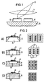
- Fig. 1 schematically shows the basic structure.
- Two (or more) sensor elements 10 are attached to substrate 15.
- Heat or IR radiation is e.g. through a lens 14 mapped on the detection surfaces of the sensor elements 10.
- This arrangement emits radiation onto one of several Sensor elements 10 shown, so that accordingly the number of sensor elements 10 a resolution according to different Solid angle ranges is possible.
- Such systems have the disadvantage that it is due to heat conduction between individual sensor elements 10 to thermal Crosstalk or crosstalk can come.
- a sensor element 10 that is not of (through an optic infrared radiation is illuminated, nevertheless emits a signal because it has heat from neighboring, from Receives heat radiation illuminated sensor elements 10.
- a sensor element can e.g. by several tenths Warm up degrees. This heat can turn into an unlit Spread out neighboring element and also close there lead an output signal. This will change the contrast of the Sensor system worse.
- thermopiles on a apply thermally poorly conductive carrier membrane, which is stretched over etching pits in the carrier substrate.
- the Etching pits are used for thermal insulation of the sensor element 10 against the substrate 15 and thus the increase in Sensitivity of the sensor system. Even with this structure however, crosstalk is detected, so that the thermal insulation of the individual sensor elements against each other is sufficient.
- only a comparatively small one Part of the substrate surface actually from sensor elements 10 covered because the formed from the back of the substrate Caustic pits do not have vertical walls that have a large spacing of the individual on the front of the substrate force attached sensor elements. This is the Detection sensitivity low, and smaller point sources can due to the image through the lens in places be mapped between sensor elements so that they cannot be detected and the sensor system is therefore unreliable is working.
- FIG. 2 shows schematically in section and in plan view not to scale structures as they are in the prior art are known.
- the sensor element is located in FIG. 2A 10 over an etching pit 24 which has sloping walls.
- the sloping walls result from the influence of the known manufacturing process through the crystal orientation in the substrate 15.
- FIG. 2B An embodiment is shown in which the etching pits 25 diamond-shaped plan with have vertical walls in the thickness direction.
- the diamond-shaped Floor plan is also created in this embodiment due to the influence of the etching process by the crystal orientation.
- Figure 2C shows an embodiment, at by an etching process from the front of the substrate Wells 26 are formed.
- 2D finally shows an embodiment in which a Gap 23 formed between sensor element 10 and substrate 15 is applied by first applying a sacrificial layer and this removed after the sensor element 10 has been formed thereon becomes. Because of the small distance is the thermal insulation of the sensor element from the substrate 15 bad, so that the signal amplitude and thus the sensitivity of the sensor system is low. Procedures that are based on the use of sacrificial layers, e.g. in DE 19 539 696 A1 or in EP 0 534 768 or in PCT / EP89 / 01082.
- the object of the invention is to create a sensor system that works reliably and a high quality Signal acquisition allowed.
- Another object of the invention is a sensor system to create something that simply checks how it works can be specified, as well as a test procedure for this.
- Another object of the invention is a sensor system to create that small in size and cheap to manufacture is.
- Fig. 3 shows embodiments in which the invention Sensor system at least several sensor elements 10 and has a substrate 15.
- the sensor system usually works with an imaging device 14.
- a such an imaging device can be a lens, a lens system, a suitable mirror device or the like be the incident heat radiation on one of the sensor elements 10 maps.
- the sensor elements 10 are preferably thermoelectric Detectors, e.g. Thermopile sensors because they are sensitive to light are and a simple signal processing allow.
- the sensor elements 10 can also be other be thermal detectors, for example pyroelectric Detectors that only change the incident heat radiation give a signal, or bolometer. Others too Sensor elements that are subject to incident heat radiation give a signal can be used.
- thermopile based sensor element denotes 15 the substrate, 46 a thermal insulation device, 41 and 42 layers of different, suitable Materials and 43 a heat absorption layer.
- the arrangement shown has a "warm end” 44 and a “cold end” End “45.
- the warm end 44 lies over the heat insulation device 46 and under the absorption layer 43. Thereby the warm end is due to the incident infrared radiation warmed up.
- the cold end 45 has in the embodiment shown a "left" and a "right” tail that each lie over the substrate 15 serving as a heat sink.
- the arrangement described ensures that the warm end 44 due to infrared radiation supported by the absorption layer 43 and the heat insulation device 46 heated while the cold end 45 or its two extensions essentially the temperature of the substrate 15 serving as a heat sink. Due to the temperature difference between the warm end 44 and cold end 45 creates a tension on the two Foothills of the cold end 45 can be tapped. height and polarity of the voltage depend among other things of the Choice of the materials of layers 41 and 42 and the quality insulation between the warm and cold ends. For reinforcement the effect can be provided several in Fig. 4 arrangements shown to connect in series. It would then the tail of the cold end 45 from one material with the tail of the cold end 45 out of the other Material. This adds up the respective Signal voltages so that a stronger effect is achieved can be.
- the sensor element includes all of the warm Ends 44 and cold ends 45 of optionally in series switched several structures according to Fig. 4.
- the actual The detection area of the sensor element corresponds to essentially that occupied by the absorption layer 43 Footprint, because in this area there is a significant warming the signal.
- the absorption layer 43 is therefore preferably designed that they are only within by the thermal insulation device 46 predetermined base area on the substrate 15 lies. The contact point of the two materials of the layers 41 and 42 lies under the absorption layer 43.
- the area occupied by the absorption layer 43 also as Sensor area 43 of the sensor element 10 are referred to.
- the absorption layer 43 equivalent area for example through a suitable surface treatment of the layers 41, 42 in the area of their contact to create over the heat insulation device 46.
- the cold ends 45 can, unlike shown in FIG. 4, also directly next to one another on the substrate 15 lie, the layers 41, 42 then approximately parallel towards the thermal insulation device 46 and under the absorption layer 43 extend.
- the sensor elements 10 are on a substrate or carrier 15 attached.
- the substrate 15 preferably has silicon on.
- the sensor elements 10 can be a line or a two-dimensional one Field attached to the substrate, or they can be placed along a track or on surfaces be the mapping of routes to be monitored and Areas through the lens 14 correspond. For example fifteen sensor elements 10 arranged in a 3x5 field be. Through suitable contacts (not in the figures shown) their respective output signals are forwarded so that they are individual for each sensor element 10 can be queried or evaluated. It far larger sensor fields are also possible. Depending on requirements can also, for example, 10x10 fields or 100x100 fields can be formed. Then they have one correspondingly finer spatial resolution.
- the substrate 15 has under the respective sensor elements 10 material cutouts 33, 35, 54. Under the gap between adjacent sensor elements 10 preferably each have a web of material 32.
- the material cutouts 33, 55, 54 serve as a heat insulation device 46 in Fig. 4.
- one Sensor system each have a material recess 33, 35, 54.
- a material recess 33, 35, 54 is under each sensor element 10 of the sensor system, a material recess 33, 35, 54 provided.
- the substrate 15 there is a material recess an elongated trench 54 provided through one of the above methods from the substrate front or the back of the substrate may have been formed.
- Several Trenches, each with a plurality of sensor elements, can preferably be used be provided in parallel.
- the substrate 15 is covered by an insulation layer 51.
- the sensor elements 10 are attached so that they are at least partially over the trench 54 lie.
- the sensor areas through the absorption layer 43 are given, lie above the trench 54.
- Reference number 55 correspondingly shows an absorption layer the absorption layer 43 in Fig. 4.
- An insulation device is located in the vicinity of a sensor element 10 52 provided. It consists of a good thermal conductor Material, for example a thin metal layer.
- the insulation device serves as a heat sink, the heat that over the insulation layer 51 to the adjacent sensor element could spread out in other directions. It is preferably attached so that it is on the one hand via material cutouts, for example trench 54 or Hole 33, 35 lies, and on the other hand over one of the substrate webs 22. It is preferably between neighboring ones Sensor elements 10.
- the insulating device 52 can also be formed by substrate bridges, which under the Isolation layer 51 and the trench 54 or larger Spanning holes. Such substrate bridges work for the heat spreading over the insulation layer 51 also as a heat sink, so that the heat in the substrate 15, 32 is derived.
- the isolation device can also be in Form of slits crossing the material recess in the insulation layer 51 or as a combination of bridges and slots are formed.
- Such slits in the insulation layer 51 interrupt the flow of heat through the insulation layer to the neighboring sensor element 10.
- the heat then spreads in the insulation layer 51 in one direction from where they are in those areas of the insulation layer 51 arrives, with the substrate 15 or with its Web 32 are connected so that the heat in this Heat sinks is absorbed.
- the insulation layer is a layer, the heat worse conducts as silicon and the electrically poorly conductive is. On the one hand, it serves the thermal and electrical Isolation and on the other hand wearing the sensor elements 10 over the material cutouts 23, 25, 44.
- the material cutouts 23, 25, 44 For example made of silicon oxide, silicon carbide and / or silicon nitride exist and is usually thinner than 1 ⁇ m. It can be trained first, and then that Material cutouts 33, 35, 54 made. This works the insulation layer, if from the back of the substrate the material recess is formed as an etch stop. If the material recess is formed from the front of the substrate the insulation layer 51, for example be pierced by a specially adapted etching process, for example by RIE (reactive ion etching, "reactive ion etching").
- Reference numeral 53 denotes self-test devices which are for a self-test function can be used. It deals are heating elements, the sensor elements 10 with Can apply heat so that it can be checked whether the sensor elements 10 produce a signal when this is applied spend as expected.
- the self-test facilities 53 can be heating resistors which are characterized by (not shown) Power lines receive electricity and then when they are flooded with electricity, and then heat the sensor elements 10 by heat radiation and / or by heat conduction over substrate 15 and any insulation layer present Warm up 51.
- the self-test facilities 53 can also be so between sensor elements 10 attached that they are two or more of the sensor elements irradiate or heat.
- the self-test facilities 53 can be designed to be individual can be controlled, or that they are controlled together become.
- Self-test devices 53 can straight lines a resistance material that is preferably parallel to an edge of a sensor element 10 along the edge extend. If multiple self-test devices 53 are provided , they can, provided an individual control is not necessary in parallel or in parallel Series are interconnected.
- the material for the self-test device 53 should be selected so that the Self-test device 53 also the function of the isolation device 52 met.
- the two facilities are then no longer provided separately, but provided as one.
- the material is to be chosen so that on the one hand there is current flow warmed, but on the other hand it has a thermal conductivity, which is better than that of the fluid (e.g. air) that is on the insulation layer 51 adjoins.
- the Thermal conductivity better than that of the insulation layer 51.
- the materials are metallic or semiconducting resistance layers, e.g. Polysilicon, crystalline silicon, Aluminum or gold, conceivable.
- This embodiment can therefore be designed so that alternately over the trench 54 one sensor element 10 each and a combined one Self-test / isolation device 52, 53 lie.
- There one Self-test device 53 the two adjacent to the trench Can apply heat to sensor elements 10, a Embodiment also look like every other device a combined self-test / heat insulation device between sensor elements 10 52, 53 is the one suitable contacting can be supplied with current, while each other (located in the other space) Device is a pure insulation device 52. This results in an inexpensive and yet more compact Structure of the sensor system.
- the self-test facilities 53 heated, so that this in turn the Heat or irradiate sensor elements 10.
- the respective sensor elements 10 a qualitative and / or output a quantitatively expected signal.
- a calibration of the sensor system is possible.
- the self-test can be comparatively short Time constants occur. This offers advantages for certain Areas of application, for example in automotive engineering. In modern automobiles, the entire Sensor technology checked when starting the vehicle. Thanks shortly The self-test according to the invention can in short time constants Time, preferably in less than 1 sec be so that when starting a vehicle a corresponding Sensor can be checked.
- the temporal pattern can for example be a sequence of two or more pulses be or a time-varying signal. Because of the are short time constants due to the low masses Signal patterns with individual pulses of less than 50 ms, preferably shorter than 5 ms, possible. So you are faster than the changes due to objects to be detected.
- control of the self-test devices described above 53 and then checking the output signals of the Sensor elements 10 are preferably made by a (not shown control.
- the sensor elements 10 described generally enter Signal out that is the intensity of the incoming heat radiation reflects quantitatively, i.e. an analog signal. Because of the fact that several sensor elements 10 are provided multiple analog signals must also be passed on or prepare. This can be done in that the analog values in the immediate vicinity of the sensor elements 10 are time-multiplexed and the resulting serial signal is output via a data line. The number of required signal output lines are reduced by this Measure considerably, in extreme cases on one.
- FIG. 6 shows an example of a relevant circuit diagram.
- 10 shows a plurality of sensor elements as a circuit diagram, each of which inputs an input signal (1 to 16) into the analog multiplexer 62. The respectively selected signal is amplified in the amplifier 63. The signal output by the amplifier 63 could already be output in this way.
- an analog sample and hold element 65 can be provided, which receives the analog signal from the amplifier 63.
- a temperature sensor 64 can also be provided, which generates an analog signal corresponding to the absolute temperature of the sensor system.
- the output signals from the temperature sensor 64 and sample-and-hold element 55 can be combined by a further multiplexer 66, so that a single analog signal appears at the data output 67, which shows the output signals of the individual sensor elements 10 and any temperature sensor 64 that may be present.
- Such an embodiment only has a single data output 67.
- a few further few connections, preferably 1 to 2 for control functions, and those for the supply voltage are required.
- Reference numeral 69 denotes the symbolically represented limitation of the sensor system. All of the components shown are located within a few millimeters. The overall system can be built up, for example, to less than 100 mm 2 . 6 shows an embodiment in which there is no analog-to-digital conversion.
- an analog-digital converter can also be provided at the output of the amplifier 63, the sample-and-hold element 65 or the multiplexer 66.
- Reference numeral 68 denotes a controller, preferably a control processor, which controls and monitors the internal processes in the sensor system.
- Fig. 6 accordingly shows an example in which the signals output by the sensor elements 10 a signal conditioning Go through 62 to 69.
- the signal processing 62 to 69 are - preferably serial - analog or digital data.
- 6 can be hybrid or be monolithic. Located in the monolithic structure the signal processing on the same substrate 15 as the sensor elements 10. In the hybrid construction is the signal conditioning 62 to 69 on its own Built up substrate or chip and with the sensor elements 10 electrically connected to the substrate 15. This one too However, the two substrates are in the immediate structure spatial proximity and especially within one Housing (symbolized by reference number 69), the surrounds the sensor system according to the invention.
- a temperature sensor 64 be provided for the absolute temperature of the substrate. With its help it becomes possible regarding the substrate temperature relative output signals of the sensor elements 10 refer to the absolute temperature, so that a qualitative refinement of the output signals of the sensor system he follows. With such a system, for example possible to capture people and them from others Differentiate between heat radiation sources, provided that this one have a temperature other than approx. 37 ° C. Besides, can determines the temperature of objects with high accuracy even if the temperature of the sensor itself is not constant.
- the above-mentioned signal conditioning 62 to 69 can also a calibration device, for example in the form of so-called "fusable links", to show the characteristic of the Adjust sensor system or its sensor elements. It can, for example, by burning individual diode sections, associated with calibration resistors, Manufacturer's zero points and reinforcements are permanent can be set so that any sensor system compatible with another in terms of its characteristic is. So it is possible to get the sensor system from the manufacturer to calibrate so that it is interchangeable with the user is without recalibration. This makes service easier essential.
- the sensor elements are usually rectangular and have Edge lengths between 40 and 500 ⁇ m. They are preferably square.
- the center distance between individual sensor elements is between 50 ⁇ m and 1000 ⁇ m.
- One as a substrate The wafer used can have a thickness between 200 and 1000 ⁇ m, preferably have between 300 and 500 microns.
- the wells 35 preferably have a depth of over 100 microns.
- Such a small sensor system can be used for different Purposes.
- One area of application is Monitoring vehicle interiors.
- the sensor system can be attached to the roof of the vehicle and its resolution (corresponding to the number of sensor elements 10) designed in this way be that it can be recognized whether individual seats in the Vehicle are occupied. According to the signal obtained in this way other vehicle functions can be controlled, for example air conditioning, airbag, etc.
- Sensor systems can also be used for building surveillance or generally used for people detection.
- the sensor system described can be constructed with or without imaging optics and the signal processing in a small transistor housing of 1 cm 3 or less volume.
Landscapes
- Physics & Mathematics (AREA)
- General Physics & Mathematics (AREA)
- Spectroscopy & Molecular Physics (AREA)
- Engineering & Computer Science (AREA)
- Microelectronics & Electronic Packaging (AREA)
- Photometry And Measurement Of Optical Pulse Characteristics (AREA)
- Radiation Pyrometers (AREA)
Abstract
Description
- Fig. 1
- den prinzipiellen Aufbau eines Sensorsystems,
- Fig. 2A-D
- mehrere nach bekannten Verfahren hergestellte Sensorsysteme,
- Fig. 3A, B
- erfindungsgemäße Ausführungsformen von Sensorsystemen in Schnitt- und Draufsicht,
- Fig. 4
- schematisch den Aufbau eines Thermopile-Sensorelements,
- Fig. 5
- in Kombination mehrere weitere erfindungsgemäße Ausführungsformen,
- Fig. 6
- das Schaltbild einer weiteren erfindungsgemäßen Ausführungsform.
- Mit 33 (Fig. 3A) ist ein Loch bezeichnet, das vorzugsweise von der Substratrückseite her im Substrat 15 gebildet werden kann. Auf der Substratvorderseite sind die Lochränder so dimensioniert, daß das Sensorelement 10 bereichsweise und insbesondere gegebenenfalls mit seinen kalten Enden 45 auf Rändern des Lochs liegt. Fig. 5 zeigt noch eine weitere Ausführungsform, unter der ein Sensorelement 10 am Substrat befestigt werden kann, diese wird später erläutert.
- Fig. 3B zeigt eine Ausführungsform der Materialaussparung, bei der auf der Substratvorderseite her eine Vertiefung 35 im Substrat ausgebildet wird, deren Dimensionierung wiederum so beschaffen sein kann, daß das Sensorelement 10 auf Ränder der Vertiefung 35 aufgesetzt und an ihnen befestigt werden kann. Auch hier kann die Befestigung am Substrat gemäß Fig. 5 erfolgen.
- Reaktives Ionenätzen in Bulk-Mikromechanik. Das Verfahren wird auch mit DRIE (= Deep Reaktive Ion Etching) bezeichnet. Hier wird vorzugsweise von der Substratrückseite her durch das Substrat hindurch ein Loch gebildet. Es handelt sich um ein Plasmaätzverfahren, mit dem ein Loch mit geraden Wänden und genau dimensionierten Abmessungen hergestellt werden kann. Es können vergleichsweise dünne, lange Löcher gebildet werden. Die einzelnen Löcher benötigen deshalb wenig Platz auf dem Substrat, so daß aufgrund von mehr Sensorelementen pro Substratfläche bzw. mehr Sensorfläche pro Substratfläche die Auflösung sowie die Flächenfüllung und damit die Empfindlichkeit erhöht werden können. In diesem Zusammenhang wird darauf hingewiesen, daß die Fig. 1 bis 5 nicht maßstäblich zu verstehen sind. Sie geben die jeweiligen Ausführungsformen nur qualitativ wieder. Durch reaktives Ionenätzen kann ein Loch 33 gemäß Fig. 3A hergestellt werden. Mit dieser Technik ist es beispielsweise möglich, in einem 500 µm dicken Wafer, der als Substrat 15 dient, Durchlöcher eines beliebigen Durchmessers, insbesondere mit Durchmessern zwischen 50 und 200 µm, regelmäßig beabstandet zu schaffen. Das Loch hat damit die Tiefe entsprechend der Dicke des Wafers, so daß das warme Ende gut isoliert ist und damit die Empfindlichkeit des Sensorelements verbessert ist. Aufgrund der nahezu senkrechten Wände müssen nur dünne Stege 32 stehenbleiben, so daß sich eine hohe Packungsdichte ergibt. In einer bevorzugten Ausführungsform werden 90 bis 99 % des Lochs mittels reaktivem Ionenätzen erzeugt. Bis zur Endtiefe (100 %) wird dann das Loch mittels eines isotropen oder anisotropen Ätzverfahrens erzeugt.
- Herstellen und Weiterbearbeiten von porösem Silizium. Hierbei wird mikromechanisch von der Substratvorderseite her gearbeitet. In einem ersten Schritt wird poröses Silizium in denjenigen Oberflächen des Substrats 15 geschaffen, in denen später die Materialaussparungen 33, 35, 54 liegen sollen. Hierzu wird ein elektro-chemisches Verfahren verwendet. Die eigentlichen Materialaussparungen werden danach hergestellt, so daß Vertiefungen 35 entsprechend Fig. 3B entstehen. Vorzugsweise werden die Vertiefungen 35 erst dann durch Abtragen des porösen Siliziums gebildet, wenn vorher auf dem porösen Silizium bzw. dem Substrat 15 das Sensorelement 10 ausgebildet wurde. Es wird dann von der Oberfläche her das poröse Silizium herausgeätzt. Auf diese Weise können Gruben einer Tiefe von größer 100 µm geschaffen werden. Bei der Verwendung von Vertiefungen 35 anstatt von Löchern 33 weist das Substrat bzw. der gesamte Aufbau nach seiner Fertigstellung eine höhere mechanische Stabilität auf. Dieses Verfahren hat den Vorteil, daß es unabhängig von der Waferdicke ist und daß bei guter Empfindlichkeit eine hohe Packungsdichte erzielt werden kann.
Claims (27)
- Sensorsystem zum Erfassen von Wärmestrahlung, miteinem Substrat (15),mehreren Sensorelementen (10), die nach Maßgabe von auf sie auftreffender Wärmestrahlung je ein elektrisches Signal ausgeben und die auf dem Substrat (15) angebracht sind,
gekennzeichnet durchzumindest eine Selbsttesteinrichtung (53) zur Erzeugung von Wärme, mit der ein oder mehrere Sensorelemente (10) erwärmt werden können. - Sensorsystem nach Anspruch 1, dadurch gekennzeichnet, daß mehrere Selbsttesteinrichtungen (53) zur Erzeugung von Wärme vorgesehen sind, die je einem Sensorelement (10) zugeordnet sind.
- Sensorsystem nach Anspruch 1 oder 2, dadurch gekennzeichnet, daß im Substrat (15) unter zumindest einem Sensorelement (10) eine Materialaussparung (33, 35, 54) vorgesehen ist.
- Sensorsystem nach Anspruch 3, dadurch gekennzeichnet, daß die Materialaussparung ein das Substrat durchsetzendes Loch (33) ist.
- Sensorsystem nach Anspruch 3, dadurch gekennzeichnet, daß die Materialaussparung eine Vertiefung (35) von der Substratvorderseite her ist.
- Sensorsystem nach einem der Ansprüche 1 bis 5, dadurch gekennzeichnet, daß das Substrat (15, 32) an seiner Oberfläche eine Isolationsschicht (51) aufweist, auf der die Sensorelemente (10) angebracht sind.
- Sensorsystem nach einem der Ansprüche 3 bis 5 und 6, dadurch gekennzeichnet, daß die Isolationsschicht (51) die Materialaussparungen (33, 35, 54) überspannt und die Sensorelemente (10) so auf der Isolationsschicht (51) angebracht sind, daß sie ganz oder teilweise über einer Materialaussparung (33, 35, 54) liegen.
- Sensorsystem nach einem der Ansprüche 1 bis 7, dadurch gekennzeichnet, daß zwischen Sensorelementen (10) eine Isoliereinrichtung (52) vorgesehen ist.
- Sensorsystem nach Anspruch 7 und 8, dadurch gekennzeichnet, daß die Isoliereinrichtung (52) aus wärmeleitendem Material auf der Isolationsschicht (51) bereichsweise über einer Materialaussparung (33, 35, 54) ausgebildet ist.
- Sensorsystem nach Anspruch 7 und 8, dadurch gekennzeichnet, daß die Isoliereinrichtung (52) ein Schlitz in der Isolationsschicht (51) im Bereich einer Materialaussparung (33, 35, 54) ist.
- Sensorsystem nach einem der Ansprüche 1 bis 10, dadurch gekennzeichnet, daß die Selbsttesteinrichtung (53) eine Einrichtung ist, die auf einen Stromfluß hin Wärme erzeugt, wobei die Selbsttesteinrichtung (53) länglich geformt und in der Nähe und vorzugsweise parallel zu einer Kante eines Sensorelements (10) angebracht ist.
- Verfahren zur Herstellung eines Substrats für ein Sensorsystem nach einem der Ansprüche 1 bis 11, das auf dem Substrat angebracht mehrere Sensorelemente aufweist, wobei unter den Sensorelementen Materialaussparungen gebildet werden,
dadurch gekennzeichnet, daßdie Materialaussparungen entweder durch OberflächenMikromechanik in porösem Silizium von der Substratvorderseite her oder durch reaktives Ionenätzen gebildet werden. - Verfahren nach Anspruch 12, dadurch gekennzeichnet, daß zur Herstellung von porösem Silizium ein elektrochemisches Verfahren verwendet wird.
- Verfahren nach Anspruch 12, dadurch gekennzeichnet, daß beim reaktiven Ionenätzen ein Plasmaätzverfahren verwendet und das Substrat von der Substratrückseite her bearbeitet wird.
- Verfahren nach Anspruch 12 oder 14, dadurch gekennzeichnet, daß beim Anwenden von reaktivem Ionenätzen das Loch bis zu einer Tiefe von 90 bis 99 % der Gesamttiefe durch reaktives Ionenätzen gebildet und bis zur Endtiefe durch isotropes oder anisotropes Ätzen erzeugt wird.
- Sensorsystem nach einem der Ansprüche 4 bis 11 und 3, dadurch gekennzeichnet, daß die Materialaussparungen (33, 35, 54) mit einem Verfahren nach einem der Ansprüche 12 bis 14 gebildet sind.
- Sensorsystem zum Erfassen von Wärmestrahlung, insbesondere nach einem der Ansprüche 1 bis 11 oder 16, miteinem Substrat (15),mehreren Sensorelementen (10), die nach Maßgabe von auf sie auftreffender Wärmestrahlung je ein elektrisches Signal ausgeben und die auf dem Substrat (15) angebracht sind,
gekennzeichnet durcheine Signalaufbereitungseinrichtung (62 - 69), die zumindest parallel vorliegende elektrische Ausgangssignale von Sensorelementen (10) in ein serielles Signal umwandelt und dieses an einem Anschluß (67) ausgibt. - Sensorsystem nach Anspruch 17, dadurch gekennzeichnet, daß die Signalaufbereitungseinrichtung (62 - 69) auf dem Substrat (10) ausgebildet ist.
- Sensorsystem nach Anspruch 17, dadurch gekennzeichnet, daß die Signalaufbereitungseinrichtung (62 - 69) auf einem eigenen Substrat ausgebildet, in unmittelbarer Nähe des Substrats (15) der Sensorelemente (10) angebracht und damit elektrisch verbunden ist.
- Sensorsystem nach einem der Ansprüche 17 bis 19, dadurch gekennzeichnet, daß es eine Temperaturmeßeinrichtung (64) aufweist, die ein Signal nach Maßgabe der absoluten Temperatur ausgibt.
- Sensorsystem nach einem der Ansprüche 1 bis 11 oder 16 bis 20, gekennzeichnet durch eine Kalibriereinrichtung zum dauerhaften Einstellen der Kennlinie zumindest eines Sensorelements (10).
- Sensorsystem nach einem der Ansprüche 1 bis 11 oder 16 bis 21, dadurch gekennzeichnet, daß mehrere Selbsttesteinrichtungen (53) vorgesehen sind, die unterschiedlich zueinander derart ausgestaltet sind, daß sie mehrere Sensorelemente (10) unterschiedlich erwärmen.
- Sensorsystem nach Anspruch 10, dadurch gekennzeichnet, daß zwischen dem als Isoliereinrichtung (52) dienenden Schlitz und dem Sensorelement (10) eine Selbsttesteinrichtung (53) vorgesehen ist.
- Selbsttestverfahren in einem Sensorsystem nach einem der Ansprüche 1 bis 11 oder 16 bis 23, dadurch gekennzeichnet, daß zumindest eine Selbsttesteinrichtung erwärmt und das Ausgangssignal zumindest eines Sensorelements überwacht wird.
- Verfahren nach Anspruch 24, dadurch gekennzeichnet, daß eine Selbsttesteinrichtung mit einem charakteristischen elektrischen Signal betrieben wird.
- Verfahren nach Anspruch 25, dadurch gekennzeichnet, daß das elektrische Signal zwei oder mehrere Impulse und/oder ein zeitveränderliches Signal aufweist.
- Verfahren nach einem der Ansprüche 24 bis 26, dadurch gekennzeichnet, daß zur Fortsetzung der Überwachung durch das Sensorsystem während des Selbsttestverfahrens vom Ausgangssignal des Sensorsystems während des Selbsttestverfahrens das erwartete charakteristische Signal aufgrund der Wirkungsweise der Selbsttesteinrichtung abgezogen wird, um das der Überwachung dienende Signal zu ermitteln.
Applications Claiming Priority (2)
| Application Number | Priority Date | Filing Date | Title |
|---|---|---|---|
| DE19735379 | 1997-08-14 | ||
| DE19735379A DE19735379B4 (de) | 1997-08-14 | 1997-08-14 | Sensorsystem und Herstellungsverfahren |
Publications (3)
| Publication Number | Publication Date |
|---|---|
| EP0898159A2 true EP0898159A2 (de) | 1999-02-24 |
| EP0898159A3 EP0898159A3 (de) | 2000-03-29 |
| EP0898159B1 EP0898159B1 (de) | 2008-02-27 |
Family
ID=7839048
Family Applications (1)
| Application Number | Title | Priority Date | Filing Date |
|---|---|---|---|
| EP98114542A Expired - Lifetime EP0898159B1 (de) | 1997-08-14 | 1998-08-03 | Sensorsystem und Herstellungsverfahren sowie Selbsttestverfahren |
Country Status (6)
| Country | Link |
|---|---|
| US (1) | US6294787B1 (de) |
| EP (1) | EP0898159B1 (de) |
| JP (1) | JP4380813B2 (de) |
| KR (1) | KR100631449B1 (de) |
| CN (1) | CN1208966A (de) |
| DE (2) | DE19735379B4 (de) |
Cited By (4)
| Publication number | Priority date | Publication date | Assignee | Title |
|---|---|---|---|---|
| WO2001048449A3 (en) * | 1999-12-24 | 2001-12-13 | Perkinelmer Optoelectronics | Method for the correction of the output signal of an infra red radiation multiple element sensor |
| EP1045233A3 (de) * | 1999-04-14 | 2002-08-28 | Nec Corporation | Funktionelle thermische Anordnung mit hoher Ansprechgeschwindigkeit und Verfahren zum Antrieb dieser Anordnung |
| EP1296122A3 (de) * | 2001-09-10 | 2003-06-11 | PerkinElmer Optoelectronics GmbH | Sensor zum berührungslosen Messen einer Temperatur |
| EP1312903A4 (de) * | 2001-03-16 | 2004-09-29 | Seiko Epson Corp | Infrarot-detektionselement und verfahren zu seiner herstellung und gerät zur messung der temperatur |
Families Citing this family (37)
| Publication number | Priority date | Publication date | Assignee | Title |
|---|---|---|---|---|
| DE19843984B4 (de) * | 1998-09-25 | 2013-10-24 | Robert Bosch Gmbh | Verfahren zur Herstellung von Strahlungssensoren |
| EP1146573A4 (de) * | 1999-11-01 | 2004-12-22 | Matsushita Electric Industrial Co Ltd | Halbleiter und seine herstellung |
| US6828172B2 (en) * | 2002-02-04 | 2004-12-07 | Delphi Technologies, Inc. | Process for a monolithically-integrated micromachined sensor and circuit |
| JP3684233B2 (ja) * | 2002-05-14 | 2005-08-17 | キヤノン株式会社 | 指紋入力装置及びその製造方法 |
| DE10243014B4 (de) * | 2002-09-17 | 2010-07-01 | Robert Bosch Gmbh | Vorrichtung zur Detektion und Vorrichtung zur Messung der Konzentration eines Stoffes |
| DE10243012B4 (de) * | 2002-09-17 | 2006-01-05 | Robert Bosch Gmbh | Vorrichtung zur Wärmedetektion und Verfahren |
| US20040187904A1 (en) * | 2003-02-05 | 2004-09-30 | General Electric Company | Apparatus for infrared radiation detection |
| JP3944465B2 (ja) * | 2003-04-11 | 2007-07-11 | 三菱電機株式会社 | 熱型赤外線検出器及び赤外線フォーカルプレーンアレイ |
| DE10320357B4 (de) * | 2003-05-07 | 2010-05-12 | Perkinelmer Optoelectronics Gmbh & Co.Kg | Strahlungssensor, Wafer, Sensorarray und Sensormodul |
| DE10321639A1 (de) * | 2003-05-13 | 2004-12-02 | Heimann Sensor Gmbh | Infrarotsensor mit optimierter Flächennutzung |
| DE10323707A1 (de) * | 2003-05-22 | 2004-12-30 | Daimlerchrysler Ag | System zur Objekt-Erfassung für Fahrzeuge |
| CA2553632A1 (en) | 2004-02-06 | 2005-08-25 | Bayer Healthcare Llc | Oxidizable species as an internal reference for biosensors and method of use |
| DE602004020883D1 (de) * | 2004-07-22 | 2009-06-10 | Bea Sa | Thermo-empfindliche Vorrichtung zur Anwesenheitsbestimmung von automatischen Türen |
| DE112006000959B4 (de) * | 2005-05-17 | 2012-03-29 | Heimann Sensor Gmbh | Thermopile Infrarot Sensorarray |
| KR101321296B1 (ko) | 2005-07-20 | 2013-10-28 | 바이엘 헬스케어 엘엘씨 | 게이트형 전류 측정법 온도 결정 방법 |
| US7683464B2 (en) * | 2005-09-13 | 2010-03-23 | Alpha And Omega Semiconductor Incorporated | Semiconductor package having dimpled plate interconnections |
| US7622796B2 (en) * | 2005-09-13 | 2009-11-24 | Alpha And Omega Semiconductor Limited | Semiconductor package having a bridged plate interconnection |
| US20070057368A1 (en) * | 2005-09-13 | 2007-03-15 | Yueh-Se Ho | Semiconductor package having plate interconnections |
| KR101477947B1 (ko) | 2005-09-30 | 2014-12-30 | 바이엘 헬스케어 엘엘씨 | 게이트형 전압 전류 측정 이온화제 및 헤마토크리트 결정 방법 |
| BRPI0717620A2 (pt) | 2006-10-24 | 2013-10-22 | Bayer Healthcare Llc | Amperometria de decaimento transitório |
| DE102007046451B4 (de) * | 2007-09-28 | 2011-08-25 | Pyreos Ltd. | Vorrichtung zur Detektion von Wärmestrahlung mit hoher Auflösung, Verfahren zum Herstellen und Verwendung der Vorrichtung |
| WO2009076302A1 (en) | 2007-12-10 | 2009-06-18 | Bayer Healthcare Llc | Control markers for auto-detection of control solution and methods of use |
| US8680658B2 (en) * | 2008-05-30 | 2014-03-25 | Alpha And Omega Semiconductor Incorporated | Conductive clip for semiconductor device package |
| US8253111B2 (en) * | 2009-12-15 | 2012-08-28 | Shimadzu Corporation | X-ray diagnostic apparatus |
| DE102010013663A1 (de) | 2010-04-01 | 2011-10-06 | Perkinelmer Technologies Gmbh & Co. Kg | Strahlungssensor |
| DE102010013661A1 (de) | 2010-04-01 | 2011-10-06 | Perkinelmer Technologies Gmbh & Co. Kg | Strahlungssensor |
| JP5638871B2 (ja) * | 2010-08-18 | 2014-12-10 | 江藤電気株式会社 | 熱流センサ |
| CN103712737B (zh) * | 2012-10-09 | 2016-03-09 | 京元电子股份有限公司 | 用于压力感测器的自我测试结构及其方法 |
| US9219185B2 (en) | 2013-12-19 | 2015-12-22 | Excelitas Technologies Singapore Pte. Ltd | CMOS integrated method for the fabrication of thermopile pixel with umbrella absorber on semiconductor substrate |
| US9373772B2 (en) | 2014-01-15 | 2016-06-21 | Excelitas Technologies Singapore Pte. Ltd. | CMOS integrated method for the release of thermopile pixel on a substrate by using anisotropic and isotropic etching |
| US9324760B2 (en) | 2014-01-21 | 2016-04-26 | Excelitas Technologies Singapore Pte. Ltd | CMOS integrated method for fabrication of thermopile pixel on semiconductor substrate with buried insulation regions |
| TWI569427B (zh) * | 2014-10-22 | 2017-02-01 | 精材科技股份有限公司 | 半導體封裝件及其製法 |
| JP6279011B2 (ja) * | 2016-05-13 | 2018-02-14 | 三菱電機株式会社 | 熱型赤外線検出器および熱型赤外線検出器の製造方法 |
| JP6819163B2 (ja) * | 2016-09-12 | 2021-01-27 | 株式会社デンソーウェーブ | 絶縁型信号伝達装置、電子機器 |
| US10914636B2 (en) | 2018-03-16 | 2021-02-09 | Ams Sensors Uk Limited | Thermopile self-test and/or self-calibration |
| JP2019168347A (ja) * | 2018-03-23 | 2019-10-03 | 三菱マテリアル株式会社 | 赤外線センサ装置 |
| DE102020209534A1 (de) | 2020-07-29 | 2022-02-03 | Robert Bosch Gesellschaft mit beschränkter Haftung | Temperatursensor für ein chirurgisches Instrument und Verfahren zu seiner Herstellung |
Family Cites Families (11)
| Publication number | Priority date | Publication date | Assignee | Title |
|---|---|---|---|---|
| US3742231A (en) * | 1971-01-07 | 1973-06-26 | Barnes Eng Co | Thermistor bolometer having a built-in source |
| US3801949A (en) * | 1973-03-08 | 1974-04-02 | Rca Corp | Thermal detector and method of making the same |
| CA1317034C (en) | 1988-09-30 | 1993-04-27 | Alliedsignal Inc. | Fabrication of oxynitride frontside microstructures |
| GB9009117D0 (en) * | 1990-04-24 | 1990-08-08 | Emi Plc Thorn | Pyroelectric detector and method of manufacturing the same |
| US5369280A (en) | 1990-04-26 | 1994-11-29 | The Commonwealth Of Australia | Semiconductor film bolometer thermal infrared detector |
| DE69221054T2 (de) * | 1991-09-27 | 1998-01-22 | Texas Instruments Inc | Lese-System und Verfahren für Infrarotdetektoranordnungen |
| US5471060A (en) * | 1993-08-23 | 1995-11-28 | Matsushita Electric Industrial Co., Ltd. | Pyroelectric infrared radiation detector and method of producing the same |
| JP3207628B2 (ja) * | 1993-09-01 | 2001-09-10 | 松下電器産業株式会社 | 焦電型赤外線センサ |
| JP3287173B2 (ja) * | 1995-04-07 | 2002-05-27 | 三菱電機株式会社 | 赤外線検出素子 |
| JPH09229853A (ja) * | 1996-02-22 | 1997-09-05 | Fuji Electric Co Ltd | 赤外線ガス分析計用検出器 |
| DE19625235A1 (de) * | 1996-06-24 | 1998-01-02 | Abb Patent Gmbh | Bewegungsmelder zur Detektion von Wärmestrahlung abgebenden, beweglichen Objekten |
-
1997
- 1997-08-14 DE DE19735379A patent/DE19735379B4/de not_active Expired - Fee Related
-
1998
- 1998-08-03 EP EP98114542A patent/EP0898159B1/de not_active Expired - Lifetime
- 1998-08-03 DE DE59814177T patent/DE59814177D1/de not_active Expired - Lifetime
- 1998-08-13 US US09/133,802 patent/US6294787B1/en not_active Expired - Lifetime
- 1998-08-13 KR KR1019980032918A patent/KR100631449B1/ko not_active Expired - Fee Related
- 1998-08-13 JP JP22881698A patent/JP4380813B2/ja not_active Expired - Fee Related
- 1998-08-14 CN CN98118357A patent/CN1208966A/zh active Pending
Cited By (8)
| Publication number | Priority date | Publication date | Assignee | Title |
|---|---|---|---|---|
| EP1045233A3 (de) * | 1999-04-14 | 2002-08-28 | Nec Corporation | Funktionelle thermische Anordnung mit hoher Ansprechgeschwindigkeit und Verfahren zum Antrieb dieser Anordnung |
| WO2001048449A3 (en) * | 1999-12-24 | 2001-12-13 | Perkinelmer Optoelectronics | Method for the correction of the output signal of an infra red radiation multiple element sensor |
| US6871999B2 (en) | 1999-12-24 | 2005-03-29 | Perkinelmer Optoelectronics Gmbh | Method for the correction of the output signal of an infra red radiation multiple element sensor |
| CN1293373C (zh) * | 1999-12-24 | 2007-01-03 | 帕尔金艾光电子股份有限公司 | 校正红外辐射多元件传感器输出信号的方法和一种红外辐射多元件传感器系统 |
| EP1312903A4 (de) * | 2001-03-16 | 2004-09-29 | Seiko Epson Corp | Infrarot-detektionselement und verfahren zu seiner herstellung und gerät zur messung der temperatur |
| EP1296122A3 (de) * | 2001-09-10 | 2003-06-11 | PerkinElmer Optoelectronics GmbH | Sensor zum berührungslosen Messen einer Temperatur |
| EP1801554A2 (de) | 2001-09-10 | 2007-06-27 | PerkinElmer Optoelectronics GmbH | Sensor zum berührungslosen Messen einer Temperatur |
| EP1801554A3 (de) * | 2001-09-10 | 2007-08-01 | PerkinElmer Optoelectronics GmbH | Sensor zum berührungslosen Messen einer Temperatur |
Also Published As
| Publication number | Publication date |
|---|---|
| US6294787B1 (en) | 2001-09-25 |
| EP0898159A3 (de) | 2000-03-29 |
| JPH11118596A (ja) | 1999-04-30 |
| DE59814177D1 (de) | 2008-04-10 |
| KR100631449B1 (ko) | 2006-12-04 |
| CN1208966A (zh) | 1999-02-24 |
| DE19735379B4 (de) | 2008-06-05 |
| JP4380813B2 (ja) | 2009-12-09 |
| EP0898159B1 (de) | 2008-02-27 |
| DE19735379A1 (de) | 1999-02-18 |
| KR19990023585A (ko) | 1999-03-25 |
Similar Documents
| Publication | Publication Date | Title |
|---|---|---|
| EP0898159B1 (de) | Sensorsystem und Herstellungsverfahren sowie Selbsttestverfahren | |
| EP3105571B1 (de) | Verfahren und sensorsystem zur messung der konzentration von gasen | |
| DE69115141T2 (de) | Oberflächenkontaktdruckwandler. | |
| DE69912685T2 (de) | Vorrichtung und Verfahren zur Normierung und Eichung einer Sensormatrix | |
| WO2006122529A2 (de) | Thermopile infrarot sensorarray | |
| DE19842403A1 (de) | Strahlungsthermometer mit mehreren Sensorelementen, Strahlungssensor und Verfahren zur Temperaturbestimmung | |
| DE4309206C1 (de) | Halbleitervorrichtung mit einem Kraft- und/oder Beschleunigungssensor | |
| WO2003027654A2 (de) | Sensorbaustein mit einem sensorelement, das von einem heizelement umgeben ist | |
| DE19932308C2 (de) | Sensor, insbesondere Thermosensor | |
| DE602004011549T2 (de) | Miniaturisierter Sensor zur Erfassung von Eigenschaften einer Flüssigkeit, insbesondere eines Schmieröls | |
| DE102008061445A1 (de) | Halbleiter und Verfahren | |
| DE10123920A1 (de) | Integriertes Mikrostruktursensorelement zur Erfassung thermodynamischer Größen eines Fluids | |
| DE19758939B4 (de) | Verfahren zur Herstellung eines Substrats, Sensorsystem | |
| WO2006103104A1 (de) | Optisches element sowie verfahren zur erfassung von strahlparametern, mit einem als pixels-matrix ausgebildeten temperatursensor | |
| EP4055358B1 (de) | Sensorelement zur erfassung einer objekttemperatur und verfahren zum bewerten der messqualität eines solchen sensorelements | |
| DE10113190B4 (de) | Feuchtesensor nach dem Taupunktprinzip auf Basis einer dünnen Membran | |
| WO2002031434A1 (de) | Vorrichtung zur erfassung einer thermisch bedingten längenausdehnung eines maschinenteils | |
| WO2003026932A1 (de) | Verfahren und vorrichtung zum erkennen eines seitenaufpralls an einem kraftfahrzeug | |
| DE10216017A1 (de) | Halbleiterbauelement | |
| DE102004018809B4 (de) | Sensoranordnung und Verfahren zur Taupunktmessung auf Basis von miniaturisierten Peltierelementen | |
| EP3124926B1 (de) | Mikroelektromechanische vorrichtung | |
| DE102009047774B4 (de) | Durchflusssensor | |
| EP1834162B1 (de) | Mikrosystemtechnisches bauelement mit einer unter dem einfluss von temperaturänderungen verformbaren einrichtung | |
| DE102005003658A1 (de) | Modular aufgebauter Infrarotstrahlungsdetektor | |
| EP1837646B1 (de) | Verfahren und Vorrichtung zur Ermittlung der Feuchte eines Gases |
Legal Events
| Date | Code | Title | Description |
|---|---|---|---|
| PUAI | Public reference made under article 153(3) epc to a published international application that has entered the european phase |
Free format text: ORIGINAL CODE: 0009012 |
|
| AK | Designated contracting states |
Kind code of ref document: A2 Designated state(s): DE FR GB IT SE |
|
| AX | Request for extension of the european patent |
Free format text: AL;LT;LV;MK;RO;SI |
|
| RIN1 | Information on inventor provided before grant (corrected) |
Inventor name: JAEHNE, ROLF Inventor name: ZABLER, ERICH Inventor name: ROTHLEY, MANFRED Inventor name: STORCK, KARLHEINZ, DIPL.-ING.(FH) Inventor name: SIMON, MARION, DR.,DIPL.-PHYS. Inventor name: SCHIEFERDECKER, JOERG, DIPL.-ING.HABIL |
|
| PUAL | Search report despatched |
Free format text: ORIGINAL CODE: 0009013 |
|
| AK | Designated contracting states |
Kind code of ref document: A3 Designated state(s): AT BE CH CY DE DK ES FI FR GB GR IE IT LI LU MC NL PT SE |
|
| AX | Request for extension of the european patent |
Free format text: AL;LT;LV;MK;RO;SI |
|
| 17P | Request for examination filed |
Effective date: 20000920 |
|
| AKX | Designation fees paid |
Free format text: DE FR GB IT SE |
|
| RAP1 | Party data changed (applicant data changed or rights of an application transferred) |
Owner name: FRAUNHOFER-GESELLSCHAFT ZUR FOERDERUNG DER ANGEWA Owner name: ROBERT BOSCH GMBH Owner name: PERKINELMER OPTOELECTRONICS GMBH |
|
| RAP1 | Party data changed (applicant data changed or rights of an application transferred) |
Owner name: FRAUNHOFER-GESELLSCHAFT ZUR FOERDERUNG DERANGEWAND Owner name: ROBERT BOSCH GMBH Owner name: PERKINELMER OPTOELECTRONICS GMBH |
|
| 17Q | First examination report despatched |
Effective date: 20031111 |
|
| RAP1 | Party data changed (applicant data changed or rights of an application transferred) |
Owner name: FRAUNHOFER-GESELLSCHAFT ZUR FOERDERUNG DER ANGEWAN Owner name: ROBERT BOSCH GMBH Owner name: PERKINELMER OPTOELECTRONICS GMBH |
|
| GRAP | Despatch of communication of intention to grant a patent |
Free format text: ORIGINAL CODE: EPIDOSNIGR1 |
|
| GRAS | Grant fee paid |
Free format text: ORIGINAL CODE: EPIDOSNIGR3 |
|
| GRAA | (expected) grant |
Free format text: ORIGINAL CODE: 0009210 |
|
| AK | Designated contracting states |
Kind code of ref document: B1 Designated state(s): DE FR GB IT SE |
|
| REG | Reference to a national code |
Ref country code: GB Ref legal event code: FG4D Free format text: NOT ENGLISH |
|
| REF | Corresponds to: |
Ref document number: 59814177 Country of ref document: DE Date of ref document: 20080410 Kind code of ref document: P |
|
| GBT | Gb: translation of ep patent filed (gb section 77(6)(a)/1977) |
Effective date: 20080430 |
|
| ET | Fr: translation filed | ||
| PG25 | Lapsed in a contracting state [announced via postgrant information from national office to epo] |
Ref country code: SE Free format text: LAPSE BECAUSE OF FAILURE TO SUBMIT A TRANSLATION OF THE DESCRIPTION OR TO PAY THE FEE WITHIN THE PRESCRIBED TIME-LIMIT Effective date: 20080527 |
|
| PLBE | No opposition filed within time limit |
Free format text: ORIGINAL CODE: 0009261 |
|
| STAA | Information on the status of an ep patent application or granted ep patent |
Free format text: STATUS: NO OPPOSITION FILED WITHIN TIME LIMIT |
|
| 26N | No opposition filed |
Effective date: 20081128 |
|
| PG25 | Lapsed in a contracting state [announced via postgrant information from national office to epo] |
Ref country code: IT Free format text: LAPSE BECAUSE OF FAILURE TO SUBMIT A TRANSLATION OF THE DESCRIPTION OR TO PAY THE FEE WITHIN THE PRESCRIBED TIME-LIMIT Effective date: 20080227 |
|
| REG | Reference to a national code |
Ref country code: DE Ref legal event code: R081 Ref document number: 59814177 Country of ref document: DE Owner name: FRAUNHOFER-GESELLSCHAFT ZUR FOERDERUNG DER ANG, DE Free format text: FORMER OWNERS: FRAUNHOFER-GESELLSCHAFT ZUR FOERDERUNG DER ANGEWANDTEN FORSCHUNG E.V., 80686 MUENCHEN, DE; PERKINELMER TECHNOLOGIES GMBH & CO. KG, 65199 WIESBADEN, DE; ROBERT BOSCH GMBH, 70469 STUTTGART, DE Effective date: 20110329 Ref country code: DE Ref legal event code: R081 Ref document number: 59814177 Country of ref document: DE Owner name: EXCELITAS TECHNOLOGIES SINGAPORE PTE LTD, SG Free format text: FORMER OWNERS: FRAUNHOFER-GESELLSCHAFT ZUR FOERDERUNG DER ANGEWANDTEN FORSCHUNG E.V., 80686 MUENCHEN, DE; PERKINELMER TECHNOLOGIES GMBH & CO. KG, 65199 WIESBADEN, DE; ROBERT BOSCH GMBH, 70469 STUTTGART, DE Effective date: 20110329 Ref country code: DE Ref legal event code: R081 Ref document number: 59814177 Country of ref document: DE Owner name: ROBERT BOSCH GMBH, DE Free format text: FORMER OWNERS: FRAUNHOFER-GESELLSCHAFT ZUR FOERDERUNG DER ANGEWANDTEN FORSCHUNG E.V., 80686 MUENCHEN, DE; PERKINELMER TECHNOLOGIES GMBH & CO. KG, 65199 WIESBADEN, DE; ROBERT BOSCH GMBH, 70469 STUTTGART, DE Effective date: 20110329 Ref country code: DE Ref legal event code: R081 Ref document number: 59814177 Country of ref document: DE Owner name: ROBERT BOSCH GMBH, DE Free format text: FORMER OWNER: FRAUNHOFER-GESELLSCHAFT ZUR FOER, PERKINELMER TECHNOLOGIES GMBH &, ROBERT BOSCH GMBH, , DE Effective date: 20110329 Ref country code: DE Ref legal event code: R081 Ref document number: 59814177 Country of ref document: DE Owner name: FRAUNHOFER-GESELLSCHAFT ZUR FOERDERUNG DER ANG, DE Free format text: FORMER OWNER: FRAUNHOFER-GESELLSCHAFT ZUR FOER, PERKINELMER TECHNOLOGIES GMBH &, ROBERT BOSCH GMBH, , DE Effective date: 20110329 Ref country code: DE Ref legal event code: R081 Ref document number: 59814177 Country of ref document: DE Owner name: EXCELITAS TECHNOLOGIES SINGAPORE PTE LTD, SG Free format text: FORMER OWNER: FRAUNHOFER-GESELLSCHAFT ZUR FOER, PERKINELMER TECHNOLOGIES GMBH &, ROBERT BOSCH GMBH, , DE Effective date: 20110329 |
|
| REG | Reference to a national code |
Ref country code: FR Ref legal event code: TQ Ref country code: FR Ref legal event code: CD |
|
| REG | Reference to a national code |
Ref country code: DE Ref legal event code: R082 Ref document number: 59814177 Country of ref document: DE Representative=s name: BEETZ & PARTNER PATENT- UND RECHTSANWAELTE, DE |
|
| REG | Reference to a national code |
Ref country code: DE Ref legal event code: R082 Ref document number: 59814177 Country of ref document: DE Representative=s name: BEETZ & PARTNER MBB, DE Effective date: 20130426 Ref country code: DE Ref legal event code: R082 Ref document number: 59814177 Country of ref document: DE Representative=s name: BEETZ & PARTNER PATENT- UND RECHTSANWAELTE, DE Effective date: 20130426 Ref country code: DE Ref legal event code: R081 Ref document number: 59814177 Country of ref document: DE Owner name: ROBERT BOSCH GMBH, DE Free format text: FORMER OWNERS: EXCELITAS TECHNOLOGIES GMBH & CO. KG, 65199 WIESBADEN, DE; FRAUNHOFER-GESELLSCHAFT ZUR FOERDERUNG DER ANGEWANDTEN FORSCHUNG E.V., 80686 MUENCHEN, DE; ROBERT BOSCH GMBH, 70469 STUTTGART, DE Effective date: 20130426 Ref country code: DE Ref legal event code: R081 Ref document number: 59814177 Country of ref document: DE Owner name: EXCELITAS TECHNOLOGIES SINGAPORE PTE LTD, SG Free format text: FORMER OWNERS: EXCELITAS TECHNOLOGIES GMBH & CO. KG, 65199 WIESBADEN, DE; FRAUNHOFER-GESELLSCHAFT ZUR FOERDERUNG DER ANGEWANDTEN FORSCHUNG E.V., 80686 MUENCHEN, DE; ROBERT BOSCH GMBH, 70469 STUTTGART, DE Effective date: 20130426 Ref country code: DE Ref legal event code: R081 Ref document number: 59814177 Country of ref document: DE Owner name: FRAUNHOFER-GESELLSCHAFT ZUR FOERDERUNG DER ANG, DE Free format text: FORMER OWNERS: EXCELITAS TECHNOLOGIES GMBH & CO. KG, 65199 WIESBADEN, DE; FRAUNHOFER-GESELLSCHAFT ZUR FOERDERUNG DER ANGEWANDTEN FORSCHUNG E.V., 80686 MUENCHEN, DE; ROBERT BOSCH GMBH, 70469 STUTTGART, DE Effective date: 20130426 Ref country code: DE Ref legal event code: R081 Ref document number: 59814177 Country of ref document: DE Owner name: ROBERT BOSCH GMBH, DE Free format text: FORMER OWNER: EXCELITAS TECHNOLOGIES GMBH & C, FRAUNHOFER-GESELLSCHAFT ZUR FOER, ROBERT BOSCH GMBH, , DE Effective date: 20130426 Ref country code: DE Ref legal event code: R081 Ref document number: 59814177 Country of ref document: DE Owner name: EXCELITAS TECHNOLOGIES SINGAPORE PTE LTD, SG Free format text: FORMER OWNER: EXCELITAS TECHNOLOGIES GMBH & C, FRAUNHOFER-GESELLSCHAFT ZUR FOER, ROBERT BOSCH GMBH, , DE Effective date: 20130426 Ref country code: DE Ref legal event code: R081 Ref document number: 59814177 Country of ref document: DE Owner name: FRAUNHOFER-GESELLSCHAFT ZUR FOERDERUNG DER ANG, DE Free format text: FORMER OWNER: EXCELITAS TECHNOLOGIES GMBH & C, FRAUNHOFER-GESELLSCHAFT ZUR FOER, ROBERT BOSCH GMBH, , DE Effective date: 20130426 |
|
| PGFP | Annual fee paid to national office [announced via postgrant information from national office to epo] |
Ref country code: DE Payment date: 20130828 Year of fee payment: 16 |
|
| PGFP | Annual fee paid to national office [announced via postgrant information from national office to epo] |
Ref country code: FR Payment date: 20130819 Year of fee payment: 16 Ref country code: GB Payment date: 20130827 Year of fee payment: 16 |
|
| REG | Reference to a national code |
Ref country code: GB Ref legal event code: 732E Free format text: REGISTERED BETWEEN 20140320 AND 20140326 |
|
| REG | Reference to a national code |
Ref country code: DE Ref legal event code: R119 Ref document number: 59814177 Country of ref document: DE |
|
| GBPC | Gb: european patent ceased through non-payment of renewal fee |
Effective date: 20140803 |
|
| REG | Reference to a national code |
Ref country code: DE Ref legal event code: R119 Ref document number: 59814177 Country of ref document: DE Effective date: 20150303 |
|
| REG | Reference to a national code |
Ref country code: FR Ref legal event code: ST Effective date: 20150430 |
|
| PG25 | Lapsed in a contracting state [announced via postgrant information from national office to epo] |
Ref country code: GB Free format text: LAPSE BECAUSE OF NON-PAYMENT OF DUE FEES Effective date: 20140803 Ref country code: DE Free format text: LAPSE BECAUSE OF NON-PAYMENT OF DUE FEES Effective date: 20150303 |
|
| PG25 | Lapsed in a contracting state [announced via postgrant information from national office to epo] |
Ref country code: FR Free format text: LAPSE BECAUSE OF NON-PAYMENT OF DUE FEES Effective date: 20140901 |