EP0895861B1 - Tête d'ejection de liquide, substrat et methode de fabrication - Google Patents
Tête d'ejection de liquide, substrat et methode de fabrication Download PDFInfo
- Publication number
- EP0895861B1 EP0895861B1 EP98114671A EP98114671A EP0895861B1 EP 0895861 B1 EP0895861 B1 EP 0895861B1 EP 98114671 A EP98114671 A EP 98114671A EP 98114671 A EP98114671 A EP 98114671A EP 0895861 B1 EP0895861 B1 EP 0895861B1
- Authority
- EP
- European Patent Office
- Prior art keywords
- movable member
- substrate
- liquid
- heat generating
- layer
- Prior art date
- Legal status (The legal status is an assumption and is not a legal conclusion. Google has not performed a legal analysis and makes no representation as to the accuracy of the status listed.)
- Expired - Lifetime
Links
- 239000007788 liquid Substances 0.000 title claims description 263
- 239000000758 substrate Substances 0.000 title claims description 120
- 238000000034 method Methods 0.000 title claims description 88
- 238000004519 manufacturing process Methods 0.000 title claims description 47
- PXHVJJICTQNCMI-UHFFFAOYSA-N Nickel Chemical compound [Ni] PXHVJJICTQNCMI-UHFFFAOYSA-N 0.000 claims description 57
- NJPPVKZQTLUDBO-UHFFFAOYSA-N novaluron Chemical compound C1=C(Cl)C(OC(F)(F)C(OC(F)(F)F)F)=CC=C1NC(=O)NC(=O)C1=C(F)C=CC=C1F NJPPVKZQTLUDBO-UHFFFAOYSA-N 0.000 claims description 37
- 239000000463 material Substances 0.000 claims description 28
- 229910052759 nickel Inorganic materials 0.000 claims description 28
- 229910052737 gold Inorganic materials 0.000 claims description 22
- 239000010931 gold Substances 0.000 claims description 22
- PCHJSUWPFVWCPO-UHFFFAOYSA-N gold Chemical compound [Au] PCHJSUWPFVWCPO-UHFFFAOYSA-N 0.000 claims description 20
- 238000007599 discharging Methods 0.000 claims description 14
- 238000000059 patterning Methods 0.000 claims description 13
- 230000015572 biosynthetic process Effects 0.000 claims description 8
- 229910003460 diamond Inorganic materials 0.000 claims description 8
- 239000010432 diamond Substances 0.000 claims description 8
- 229910052581 Si3N4 Inorganic materials 0.000 claims description 7
- VNWKTOKETHGBQD-UHFFFAOYSA-N methane Chemical compound C VNWKTOKETHGBQD-UHFFFAOYSA-N 0.000 claims description 7
- HQVNEWCFYHHQES-UHFFFAOYSA-N silicon nitride Chemical compound N12[Si]34N5[Si]62N3[Si]51N64 HQVNEWCFYHHQES-UHFFFAOYSA-N 0.000 claims description 6
- 229910003481 amorphous carbon Inorganic materials 0.000 claims description 5
- 229910052751 metal Inorganic materials 0.000 claims description 5
- 239000002184 metal Substances 0.000 claims description 5
- 238000010030 laminating Methods 0.000 claims description 3
- 238000010438 heat treatment Methods 0.000 claims description 2
- 239000004020 conductor Substances 0.000 claims 1
- HBMJWWWQQXIZIP-UHFFFAOYSA-N silicon carbide Chemical compound [Si+]#[C-] HBMJWWWQQXIZIP-UHFFFAOYSA-N 0.000 claims 1
- 229910010271 silicon carbide Inorganic materials 0.000 claims 1
- 239000010410 layer Substances 0.000 description 83
- 239000010408 film Substances 0.000 description 45
- 230000008569 process Effects 0.000 description 15
- 239000005380 borophosphosilicate glass Substances 0.000 description 10
- 238000004544 sputter deposition Methods 0.000 description 10
- 238000005187 foaming Methods 0.000 description 9
- 238000011161 development Methods 0.000 description 8
- 230000018109 developmental process Effects 0.000 description 8
- KRHYYFGTRYWZRS-UHFFFAOYSA-N Fluorane Chemical compound F KRHYYFGTRYWZRS-UHFFFAOYSA-N 0.000 description 6
- 230000000694 effects Effects 0.000 description 6
- 238000005530 etching Methods 0.000 description 6
- 238000000926 separation method Methods 0.000 description 6
- 229910052715 tantalum Inorganic materials 0.000 description 6
- GUVRBAGPIYLISA-UHFFFAOYSA-N tantalum atom Chemical compound [Ta] GUVRBAGPIYLISA-UHFFFAOYSA-N 0.000 description 6
- 238000011144 upstream manufacturing Methods 0.000 description 6
- VYPSYNLAJGMNEJ-UHFFFAOYSA-N Silicium dioxide Chemical compound O=[Si]=O VYPSYNLAJGMNEJ-UHFFFAOYSA-N 0.000 description 5
- 238000004299 exfoliation Methods 0.000 description 5
- 239000000203 mixture Substances 0.000 description 5
- 229910052814 silicon oxide Inorganic materials 0.000 description 5
- 230000002463 transducing effect Effects 0.000 description 5
- XUIMIQQOPSSXEZ-UHFFFAOYSA-N Silicon Chemical compound [Si] XUIMIQQOPSSXEZ-UHFFFAOYSA-N 0.000 description 4
- 239000002585 base Substances 0.000 description 4
- 239000007767 bonding agent Substances 0.000 description 4
- 230000001902 propagating effect Effects 0.000 description 4
- 239000010703 silicon Substances 0.000 description 4
- 229910052710 silicon Inorganic materials 0.000 description 4
- 239000003513 alkali Substances 0.000 description 3
- 238000009835 boiling Methods 0.000 description 3
- 239000003795 chemical substances by application Substances 0.000 description 3
- 239000006260 foam Substances 0.000 description 3
- 230000004927 fusion Effects 0.000 description 3
- 239000007789 gas Substances 0.000 description 3
- 238000003475 lamination Methods 0.000 description 3
- 230000000704 physical effect Effects 0.000 description 3
- 238000005268 plasma chemical vapour deposition Methods 0.000 description 3
- 239000002210 silicon-based material Substances 0.000 description 3
- 239000000126 substance Substances 0.000 description 3
- 238000001039 wet etching Methods 0.000 description 3
- QGZKDVFQNNGYKY-UHFFFAOYSA-N Ammonia Chemical compound N QGZKDVFQNNGYKY-UHFFFAOYSA-N 0.000 description 2
- IJGRMHOSHXDMSA-UHFFFAOYSA-N Atomic nitrogen Chemical compound N#N IJGRMHOSHXDMSA-UHFFFAOYSA-N 0.000 description 2
- MHAJPDPJQMAIIY-UHFFFAOYSA-N Hydrogen peroxide Chemical compound OO MHAJPDPJQMAIIY-UHFFFAOYSA-N 0.000 description 2
- 238000009825 accumulation Methods 0.000 description 2
- 229910052782 aluminium Inorganic materials 0.000 description 2
- XAGFODPZIPBFFR-UHFFFAOYSA-N aluminium Chemical compound [Al] XAGFODPZIPBFFR-UHFFFAOYSA-N 0.000 description 2
- QVGXLLKOCUKJST-UHFFFAOYSA-N atomic oxygen Chemical compound [O] QVGXLLKOCUKJST-UHFFFAOYSA-N 0.000 description 2
- 230000008901 benefit Effects 0.000 description 2
- 230000008859 change Effects 0.000 description 2
- 230000000295 complement effect Effects 0.000 description 2
- 238000007598 dipping method Methods 0.000 description 2
- 238000006073 displacement reaction Methods 0.000 description 2
- 239000012535 impurity Substances 0.000 description 2
- 238000010348 incorporation Methods 0.000 description 2
- 238000009413 insulation Methods 0.000 description 2
- 239000007769 metal material Substances 0.000 description 2
- 239000001301 oxygen Substances 0.000 description 2
- 229910052760 oxygen Inorganic materials 0.000 description 2
- 238000012545 processing Methods 0.000 description 2
- 230000001105 regulatory effect Effects 0.000 description 2
- 239000004065 semiconductor Substances 0.000 description 2
- 238000004528 spin coating Methods 0.000 description 2
- 230000002195 synergetic effect Effects 0.000 description 2
- OKTJSMMVPCPJKN-UHFFFAOYSA-N Carbon Chemical compound [C] OKTJSMMVPCPJKN-UHFFFAOYSA-N 0.000 description 1
- 239000004642 Polyimide Substances 0.000 description 1
- BLRPTPMANUNPDV-UHFFFAOYSA-N Silane Chemical compound [SiH4] BLRPTPMANUNPDV-UHFFFAOYSA-N 0.000 description 1
- LRTTZMZPZHBOPO-UHFFFAOYSA-N [B].[B].[Hf] Chemical compound [B].[B].[Hf] LRTTZMZPZHBOPO-UHFFFAOYSA-N 0.000 description 1
- 239000002253 acid Substances 0.000 description 1
- 230000009471 action Effects 0.000 description 1
- 239000000853 adhesive Substances 0.000 description 1
- 239000000956 alloy Substances 0.000 description 1
- 229910045601 alloy Inorganic materials 0.000 description 1
- RVSGESPTHDDNTH-UHFFFAOYSA-N alumane;tantalum Chemical compound [AlH3].[Ta] RVSGESPTHDDNTH-UHFFFAOYSA-N 0.000 description 1
- 229910021529 ammonia Inorganic materials 0.000 description 1
- 230000003466 anti-cipated effect Effects 0.000 description 1
- 238000004380 ashing Methods 0.000 description 1
- 229910052799 carbon Inorganic materials 0.000 description 1
- 238000005229 chemical vapour deposition Methods 0.000 description 1
- 239000011248 coating agent Substances 0.000 description 1
- 238000000576 coating method Methods 0.000 description 1
- 239000000470 constituent Substances 0.000 description 1
- 230000001276 controlling effect Effects 0.000 description 1
- 238000007796 conventional method Methods 0.000 description 1
- 238000005520 cutting process Methods 0.000 description 1
- 230000001419 dependent effect Effects 0.000 description 1
- 230000008034 disappearance Effects 0.000 description 1
- 238000001312 dry etching Methods 0.000 description 1
- 238000005323 electroforming Methods 0.000 description 1
- 230000002708 enhancing effect Effects 0.000 description 1
- 238000001704 evaporation Methods 0.000 description 1
- 230000008020 evaporation Effects 0.000 description 1
- 238000009432 framing Methods 0.000 description 1
- -1 iridium-tantalum-aluminum Chemical compound 0.000 description 1
- 229910052757 nitrogen Inorganic materials 0.000 description 1
- 239000011368 organic material Substances 0.000 description 1
- 238000001020 plasma etching Methods 0.000 description 1
- 229920002492 poly(sulfone) Polymers 0.000 description 1
- 229920001721 polyimide Polymers 0.000 description 1
- NNFCIKHAZHQZJG-UHFFFAOYSA-N potassium cyanide Chemical compound [K+].N#[C-] NNFCIKHAZHQZJG-UHFFFAOYSA-N 0.000 description 1
- 230000005855 radiation Effects 0.000 description 1
- 230000009467 reduction Effects 0.000 description 1
- 230000000717 retained effect Effects 0.000 description 1
- 238000007789 sealing Methods 0.000 description 1
- 230000035939 shock Effects 0.000 description 1
- 229910000077 silane Inorganic materials 0.000 description 1
- LIVNPJMFVYWSIS-UHFFFAOYSA-N silicon monoxide Chemical compound [Si-]#[O+] LIVNPJMFVYWSIS-UHFFFAOYSA-N 0.000 description 1
- 239000002356 single layer Substances 0.000 description 1
- 239000002344 surface layer Substances 0.000 description 1
- MZLGASXMSKOWSE-UHFFFAOYSA-N tantalum nitride Chemical compound [Ta]#N MZLGASXMSKOWSE-UHFFFAOYSA-N 0.000 description 1
- 239000004753 textile Substances 0.000 description 1
- 239000010409 thin film Substances 0.000 description 1
Images


Classifications
-
- B—PERFORMING OPERATIONS; TRANSPORTING
- B41—PRINTING; LINING MACHINES; TYPEWRITERS; STAMPS
- B41J—TYPEWRITERS; SELECTIVE PRINTING MECHANISMS, i.e. MECHANISMS PRINTING OTHERWISE THAN FROM A FORME; CORRECTION OF TYPOGRAPHICAL ERRORS
- B41J2/00—Typewriters or selective printing mechanisms characterised by the printing or marking process for which they are designed
- B41J2/005—Typewriters or selective printing mechanisms characterised by the printing or marking process for which they are designed characterised by bringing liquid or particles selectively into contact with a printing material
- B41J2/01—Ink jet
- B41J2/135—Nozzles
- B41J2/14—Structure thereof only for on-demand ink jet heads
- B41J2/14016—Structure of bubble jet print heads
- B41J2/14088—Structure of heating means
- B41J2/14112—Resistive element
- B41J2/14129—Layer structure
-
- B—PERFORMING OPERATIONS; TRANSPORTING
- B41—PRINTING; LINING MACHINES; TYPEWRITERS; STAMPS
- B41J—TYPEWRITERS; SELECTIVE PRINTING MECHANISMS, i.e. MECHANISMS PRINTING OTHERWISE THAN FROM A FORME; CORRECTION OF TYPOGRAPHICAL ERRORS
- B41J2/00—Typewriters or selective printing mechanisms characterised by the printing or marking process for which they are designed
- B41J2/005—Typewriters or selective printing mechanisms characterised by the printing or marking process for which they are designed characterised by bringing liquid or particles selectively into contact with a printing material
- B41J2/01—Ink jet
- B41J2/135—Nozzles
- B41J2/14—Structure thereof only for on-demand ink jet heads
- B41J2/14016—Structure of bubble jet print heads
- B41J2/14024—Assembling head parts
-
- B—PERFORMING OPERATIONS; TRANSPORTING
- B41—PRINTING; LINING MACHINES; TYPEWRITERS; STAMPS
- B41J—TYPEWRITERS; SELECTIVE PRINTING MECHANISMS, i.e. MECHANISMS PRINTING OTHERWISE THAN FROM A FORME; CORRECTION OF TYPOGRAPHICAL ERRORS
- B41J2/00—Typewriters or selective printing mechanisms characterised by the printing or marking process for which they are designed
- B41J2/005—Typewriters or selective printing mechanisms characterised by the printing or marking process for which they are designed characterised by bringing liquid or particles selectively into contact with a printing material
- B41J2/01—Ink jet
- B41J2/135—Nozzles
- B41J2/14—Structure thereof only for on-demand ink jet heads
- B41J2/14016—Structure of bubble jet print heads
- B41J2/14032—Structure of the pressure chamber
- B41J2/14048—Movable member in the chamber
-
- B—PERFORMING OPERATIONS; TRANSPORTING
- B41—PRINTING; LINING MACHINES; TYPEWRITERS; STAMPS
- B41J—TYPEWRITERS; SELECTIVE PRINTING MECHANISMS, i.e. MECHANISMS PRINTING OTHERWISE THAN FROM A FORME; CORRECTION OF TYPOGRAPHICAL ERRORS
- B41J2/00—Typewriters or selective printing mechanisms characterised by the printing or marking process for which they are designed
- B41J2/005—Typewriters or selective printing mechanisms characterised by the printing or marking process for which they are designed characterised by bringing liquid or particles selectively into contact with a printing material
- B41J2/01—Ink jet
- B41J2/135—Nozzles
- B41J2/16—Production of nozzles
- B41J2/1601—Production of bubble jet print heads
- B41J2/1604—Production of bubble jet print heads of the edge shooter type
-
- B—PERFORMING OPERATIONS; TRANSPORTING
- B41—PRINTING; LINING MACHINES; TYPEWRITERS; STAMPS
- B41J—TYPEWRITERS; SELECTIVE PRINTING MECHANISMS, i.e. MECHANISMS PRINTING OTHERWISE THAN FROM A FORME; CORRECTION OF TYPOGRAPHICAL ERRORS
- B41J2/00—Typewriters or selective printing mechanisms characterised by the printing or marking process for which they are designed
- B41J2/005—Typewriters or selective printing mechanisms characterised by the printing or marking process for which they are designed characterised by bringing liquid or particles selectively into contact with a printing material
- B41J2/01—Ink jet
- B41J2/135—Nozzles
- B41J2/16—Production of nozzles
- B41J2/1621—Manufacturing processes
- B41J2/1623—Manufacturing processes bonding and adhesion
-
- B—PERFORMING OPERATIONS; TRANSPORTING
- B41—PRINTING; LINING MACHINES; TYPEWRITERS; STAMPS
- B41J—TYPEWRITERS; SELECTIVE PRINTING MECHANISMS, i.e. MECHANISMS PRINTING OTHERWISE THAN FROM A FORME; CORRECTION OF TYPOGRAPHICAL ERRORS
- B41J2/00—Typewriters or selective printing mechanisms characterised by the printing or marking process for which they are designed
- B41J2/005—Typewriters or selective printing mechanisms characterised by the printing or marking process for which they are designed characterised by bringing liquid or particles selectively into contact with a printing material
- B41J2/01—Ink jet
- B41J2/135—Nozzles
- B41J2/16—Production of nozzles
- B41J2/1621—Manufacturing processes
- B41J2/1625—Manufacturing processes electroforming
-
- B—PERFORMING OPERATIONS; TRANSPORTING
- B41—PRINTING; LINING MACHINES; TYPEWRITERS; STAMPS
- B41J—TYPEWRITERS; SELECTIVE PRINTING MECHANISMS, i.e. MECHANISMS PRINTING OTHERWISE THAN FROM A FORME; CORRECTION OF TYPOGRAPHICAL ERRORS
- B41J2/00—Typewriters or selective printing mechanisms characterised by the printing or marking process for which they are designed
- B41J2/005—Typewriters or selective printing mechanisms characterised by the printing or marking process for which they are designed characterised by bringing liquid or particles selectively into contact with a printing material
- B41J2/01—Ink jet
- B41J2/135—Nozzles
- B41J2/16—Production of nozzles
- B41J2/1621—Manufacturing processes
- B41J2/1626—Manufacturing processes etching
- B41J2/1628—Manufacturing processes etching dry etching
-
- B—PERFORMING OPERATIONS; TRANSPORTING
- B41—PRINTING; LINING MACHINES; TYPEWRITERS; STAMPS
- B41J—TYPEWRITERS; SELECTIVE PRINTING MECHANISMS, i.e. MECHANISMS PRINTING OTHERWISE THAN FROM A FORME; CORRECTION OF TYPOGRAPHICAL ERRORS
- B41J2/00—Typewriters or selective printing mechanisms characterised by the printing or marking process for which they are designed
- B41J2/005—Typewriters or selective printing mechanisms characterised by the printing or marking process for which they are designed characterised by bringing liquid or particles selectively into contact with a printing material
- B41J2/01—Ink jet
- B41J2/135—Nozzles
- B41J2/16—Production of nozzles
- B41J2/1621—Manufacturing processes
- B41J2/1626—Manufacturing processes etching
- B41J2/1629—Manufacturing processes etching wet etching
-
- B—PERFORMING OPERATIONS; TRANSPORTING
- B41—PRINTING; LINING MACHINES; TYPEWRITERS; STAMPS
- B41J—TYPEWRITERS; SELECTIVE PRINTING MECHANISMS, i.e. MECHANISMS PRINTING OTHERWISE THAN FROM A FORME; CORRECTION OF TYPOGRAPHICAL ERRORS
- B41J2/00—Typewriters or selective printing mechanisms characterised by the printing or marking process for which they are designed
- B41J2/005—Typewriters or selective printing mechanisms characterised by the printing or marking process for which they are designed characterised by bringing liquid or particles selectively into contact with a printing material
- B41J2/01—Ink jet
- B41J2/135—Nozzles
- B41J2/16—Production of nozzles
- B41J2/1621—Manufacturing processes
- B41J2/1631—Manufacturing processes photolithography
-
- B—PERFORMING OPERATIONS; TRANSPORTING
- B41—PRINTING; LINING MACHINES; TYPEWRITERS; STAMPS
- B41J—TYPEWRITERS; SELECTIVE PRINTING MECHANISMS, i.e. MECHANISMS PRINTING OTHERWISE THAN FROM A FORME; CORRECTION OF TYPOGRAPHICAL ERRORS
- B41J2/00—Typewriters or selective printing mechanisms characterised by the printing or marking process for which they are designed
- B41J2/005—Typewriters or selective printing mechanisms characterised by the printing or marking process for which they are designed characterised by bringing liquid or particles selectively into contact with a printing material
- B41J2/01—Ink jet
- B41J2/135—Nozzles
- B41J2/16—Production of nozzles
- B41J2/1621—Manufacturing processes
- B41J2/1635—Manufacturing processes dividing the wafer into individual chips
-
- B—PERFORMING OPERATIONS; TRANSPORTING
- B41—PRINTING; LINING MACHINES; TYPEWRITERS; STAMPS
- B41J—TYPEWRITERS; SELECTIVE PRINTING MECHANISMS, i.e. MECHANISMS PRINTING OTHERWISE THAN FROM A FORME; CORRECTION OF TYPOGRAPHICAL ERRORS
- B41J2/00—Typewriters or selective printing mechanisms characterised by the printing or marking process for which they are designed
- B41J2/005—Typewriters or selective printing mechanisms characterised by the printing or marking process for which they are designed characterised by bringing liquid or particles selectively into contact with a printing material
- B41J2/01—Ink jet
- B41J2/135—Nozzles
- B41J2/16—Production of nozzles
- B41J2/1621—Manufacturing processes
- B41J2/164—Manufacturing processes thin film formation
- B41J2/1642—Manufacturing processes thin film formation thin film formation by CVD [chemical vapor deposition]
-
- B—PERFORMING OPERATIONS; TRANSPORTING
- B41—PRINTING; LINING MACHINES; TYPEWRITERS; STAMPS
- B41J—TYPEWRITERS; SELECTIVE PRINTING MECHANISMS, i.e. MECHANISMS PRINTING OTHERWISE THAN FROM A FORME; CORRECTION OF TYPOGRAPHICAL ERRORS
- B41J2/00—Typewriters or selective printing mechanisms characterised by the printing or marking process for which they are designed
- B41J2/005—Typewriters or selective printing mechanisms characterised by the printing or marking process for which they are designed characterised by bringing liquid or particles selectively into contact with a printing material
- B41J2/01—Ink jet
- B41J2/135—Nozzles
- B41J2/16—Production of nozzles
- B41J2/1621—Manufacturing processes
- B41J2/164—Manufacturing processes thin film formation
- B41J2/1645—Manufacturing processes thin film formation thin film formation by spincoating
-
- B—PERFORMING OPERATIONS; TRANSPORTING
- B41—PRINTING; LINING MACHINES; TYPEWRITERS; STAMPS
- B41J—TYPEWRITERS; SELECTIVE PRINTING MECHANISMS, i.e. MECHANISMS PRINTING OTHERWISE THAN FROM A FORME; CORRECTION OF TYPOGRAPHICAL ERRORS
- B41J2/00—Typewriters or selective printing mechanisms characterised by the printing or marking process for which they are designed
- B41J2/005—Typewriters or selective printing mechanisms characterised by the printing or marking process for which they are designed characterised by bringing liquid or particles selectively into contact with a printing material
- B41J2/01—Ink jet
- B41J2/135—Nozzles
- B41J2/16—Production of nozzles
- B41J2/1621—Manufacturing processes
- B41J2/164—Manufacturing processes thin film formation
- B41J2/1646—Manufacturing processes thin film formation thin film formation by sputtering
-
- B—PERFORMING OPERATIONS; TRANSPORTING
- B41—PRINTING; LINING MACHINES; TYPEWRITERS; STAMPS
- B41J—TYPEWRITERS; SELECTIVE PRINTING MECHANISMS, i.e. MECHANISMS PRINTING OTHERWISE THAN FROM A FORME; CORRECTION OF TYPOGRAPHICAL ERRORS
- B41J2202/00—Embodiments of or processes related to ink-jet or thermal heads
- B41J2202/01—Embodiments of or processes related to ink-jet heads
- B41J2202/03—Specific materials used
-
- Y—GENERAL TAGGING OF NEW TECHNOLOGICAL DEVELOPMENTS; GENERAL TAGGING OF CROSS-SECTIONAL TECHNOLOGIES SPANNING OVER SEVERAL SECTIONS OF THE IPC; TECHNICAL SUBJECTS COVERED BY FORMER USPC CROSS-REFERENCE ART COLLECTIONS [XRACs] AND DIGESTS
- Y10—TECHNICAL SUBJECTS COVERED BY FORMER USPC
- Y10S—TECHNICAL SUBJECTS COVERED BY FORMER USPC CROSS-REFERENCE ART COLLECTIONS [XRACs] AND DIGESTS
- Y10S29/00—Metal working
- Y10S29/016—Method or apparatus with etching
-
- Y—GENERAL TAGGING OF NEW TECHNOLOGICAL DEVELOPMENTS; GENERAL TAGGING OF CROSS-SECTIONAL TECHNOLOGIES SPANNING OVER SEVERAL SECTIONS OF THE IPC; TECHNICAL SUBJECTS COVERED BY FORMER USPC CROSS-REFERENCE ART COLLECTIONS [XRACs] AND DIGESTS
- Y10—TECHNICAL SUBJECTS COVERED BY FORMER USPC
- Y10T—TECHNICAL SUBJECTS COVERED BY FORMER US CLASSIFICATION
- Y10T29/00—Metal working
- Y10T29/49—Method of mechanical manufacture
- Y10T29/49002—Electrical device making
- Y10T29/49082—Resistor making
- Y10T29/49083—Heater type
-
- Y—GENERAL TAGGING OF NEW TECHNOLOGICAL DEVELOPMENTS; GENERAL TAGGING OF CROSS-SECTIONAL TECHNOLOGIES SPANNING OVER SEVERAL SECTIONS OF THE IPC; TECHNICAL SUBJECTS COVERED BY FORMER USPC CROSS-REFERENCE ART COLLECTIONS [XRACs] AND DIGESTS
- Y10—TECHNICAL SUBJECTS COVERED BY FORMER USPC
- Y10T—TECHNICAL SUBJECTS COVERED BY FORMER US CLASSIFICATION
- Y10T29/00—Metal working
- Y10T29/49—Method of mechanical manufacture
- Y10T29/49401—Fluid pattern dispersing device making, e.g., ink jet
Definitions
- the present invention relates to a method for manufacturing a liquid discharge head and to a liquid discharge head that discharges a desired liquid by the creation of bubbles by the application of thermal energy that acts upon the liquid. More particularly, the invention relates to a liquid discharge head provided with a movable member which is displaceable by the utilization of created bubbles, and to the method of manufacture therefor as well.
- the term "recording" in the description of the present invention means not only the provision of images having characters, graphics, or other meaningful representation on a recording medium, but also, the provision of those images that do not present any particular meaning, such as patterns, on it.
- bubble jet recording method which is an ink jet recording method whereby to form images on a recording medium by discharging ink from discharge ports using acting force exerted by the change of states of ink accompanied by the abrupt voluminal changes (creation of bubbles), and to form images on a recording medium by the discharged ink that adheres to it.
- the recording apparatus that uses the bubble jet recording method, it is generally practiced to provide, as disclosed in the specifications of Japanese Patent Laid-Open Application No. 54-059936 and Japanese Patent Laid-Open Application No.
- the head that executes this recording method makes it possible to arrange the discharge ports for discharging ink in high density, with the excellent advantage, among many others, that images are made recordable in high resolution, and that color images are easily obtainable by use of a smaller apparatus.
- the bubble jet recording method is widely utilized for office equipment, such as a printer, a copying machine, a facsimile equipment. Further, this method is utilized for an industrial system, such as a textile printing system.
- the conventional liquid discharge head is structured with the movable member and the base unit thereof formed as individual bodies, respectively, as described above. Then, the movable member is positioned to the elemental substrate. After that, the movable member is bonded to the base unit by the application of gold bonding or adhesive agent.
- a method for manufacturing a liquid discharge head comprising the features summarized in the pre-characterizing clause of claim 1 and a liquid discharge head comprising the features summarized in the pre-characterizing clauses of claims 19 and 20 are known from document US-A-5278585 and document EP-A-0737582. According to these documents, the liquid discharge head is manufactured by manufacturing the substrate and the movable member separately, so requiring them to be positioned and connected precisely.
- Document JP-A-63199972 proposes a manufacturing method of a movable valve member.
- this movable valve member is not formed on a substrate with heat generating members.
- Document GB-A-2306399 discloses a manufacturing method of an active movable member of a liquid discharge head.
- the movable member is not arranged such that it faces the heat generating member on the substrate.
- the present invention is designed. It is an object of the invention to provide a method for manufacturing a liquid discharge head whereby to make the interior of each liquid flow path finer in higher precision. Moreover, it is an object of the invention to provide improved liquid discharge heads.
- the movable portion of the movable member is separated from the substrate after the formation of the movable member on the substrate. Then, the movable member is incorporated in the liquid discharge head. As a result, there is no need for the process to position the movable member to the substrate as the member that functions as a different body, hence implementing arranging each interior of many numbers of the liquid flow paths finer in higher precision.
- upstream and downstream referred to in the description of the present invention are used as expression with respect to the flow direction of liquid from the supply source of liquid to the discharge port through the bubble generating area (or the movable member) or the structural direction thereof.
- downstream side related to the bubble itself represents the portion of the bubble on the discharge port side, which mainly acts upon the discharge of droplet directly. More specifically, it means the downstream side of the above-mentioned flow direction or the structural direction with respect to the center of each bubble or the bubble that may be created on the area of the downstream side of the area center of a heat generating member.
- separation walls means, in a broader sense, the walls (which may include the movable member) which are provided to divide the bubble generating area and the area that is communicated with a discharge port directly on a broader sense, and this term means, in a narrower sense, those which divide the flow path that includes the bubble generating area and the liquid flow path which is communicated with the discharge port in order to prevent the mixture of liquids each residing in the respective areas.
- the term "the teeth of a comb" referred to in the description of the present invention means the configuration in which the fulcrum of the movable member is formed by a shareable member, and then, the front of the free end thereof is in a state of being released.
- Figs. 1A to 1D are views which illustrate the discharge principle of a liquid discharge head in accordance with the present invention. Also, Fig. 2 is a partially broken perspective view which shows the liquid discharge head represented in Figs. 1A to 1D.
- the liquid discharge head is provided with a heat generating member 2 (for the present example, a heat generating resistor in a shape of 40 ⁇ m ⁇ 105 ⁇ m) that enables thermal energy to act upon liquid as a discharge energy generating device for discharging liquid, which is arranged on the elemental substrate 1.
- a heat generating member 2 for the present example, a heat generating resistor in a shape of 40 ⁇ m ⁇ 105 ⁇ m
- the liquid flow path 10 is arranged corresponding to the heat generating member 2.
- the liquid flow path 10 is communicated with the discharge port 18, it is communicated with a common liquid chamber 13 from which liquid is supplied to a plurality of liquid flow paths 10.
- Each of the liquid flow paths 10 receives liquid from the common liquid chamber 13 in an amount corresponding to the amount of the liquid that has been discharged from the discharge port 18.
- the plate type movable member 31 formed by elastic metal material or the like, which is provided with a plane portion, is arranged in a cantilever fashion so as to face the heat generating member 2 described earlier.
- One end of the movable member is fixed on the stand (supporting member) or the like formed by patterning a photosensitive resign or the like on the walls of the liquid flow path 10 or on the elemental substrate 1. In this manner, the movable member is supported, and at the same time, the fulcrum (fulcrum portion) 33 is arranged.
- the movable member 31 being formed in a shape of teeth of a comb, it becomes possible to produce movable members 31 easily at lower costs. It also becomes easier to align each of them with the stand, respectively.
- the movable member 31 is arranged in a position to face the heat generating member 2 with a gap of approximately 15 pm with the heat generating member 2 so as to cover it and provide the fulcrum (fulcrum portion: fixed end) 33 on the upstream side of a large flow running from the common liquid chamber 13 to the discharge port 18 side through the movable member 31 by the operation of liquid discharge, and the free end (free end portion) 32 on the downstream side with respect to this fulcrum 33. Between the heat generating member 2 and the movable member 31 is the bubble generating area 11.
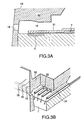
- Figs. 3A and 3B are views which illustrate the liquid discharge head manufactured by a method for manufacturing liquid discharge heads in accordance with another embodiment of the present invention: Fig. 3A is a cross-sectional view taken in the liquid flow direction; and Fig. 3B is a sectionally perspective view.
- the present embodiment comprises the heat generating member 2 that creates bubbles by the application of heat; the substrate 1 on which the heat generating members 2 are incorporated; the discharge ports 18 for discharging liquid; the orifice plate 19 having the discharge ports 18 formed therefor to determine the discharge direction of liquid; liquid flow paths 10 for supplying the discharge liquid to each of the discharge ports 18; the grooved member 50 that forms each of the liquid flow paths 10, the movable member 31 displaceable along the creation of bubbles on each of the heat generating members 2; and the pedestal portions 7 that supports the movable members 31, respectively.
- the groove walls 52 that separate a plurality of liquid flow paths 10 from each other are arranged to extend in the direction toward the orifice plate 19, and formed integrally with the orifice plate 19.
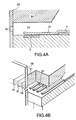
- FIGs. 4A and 4B are views which illustrate the liquid discharge head manufactured by the method for manufacturing liquid discharge heads in accordance with still another embodiment of the present invention: Fig. 4A is a cross-sectional view taken in the liquid flow direction; and Fig. 4B is a sectionally perspective view.
- the orifice plate 29 and the grooved member 51 are prepared as individual bodies in accordance with the present embodiment. Then, the groove walls 52 that separate the plural liquid flow paths 10 from each other are arranged to extend in the direction of the orifice plate 29, and bonded to the orifice plate 29 by use of a bonding agent or the like.
- Figs. 5A to 5J are views which illustrate the method for manufacturing the liquid discharge head represented in Figs. 3A and 3B in accordance with a first embodiment of the present invention.
- the state of grooved film lamination is simplified for representation.
- the electrode layer 210 formed by TiW layer or nickel layer is arranged by means of sputtering method or the like (Fig. 5B).
- the electrode layer 210 is coated by resist 211. After that, the resist 211 is patterned corresponding to the configuration of the pedestal portion 7 (Fig. 5C).
- the resist 211 is removed to make the pedestal portion 7 formed by gold 211 (Fig. 5E).
- the fusion (evaporation) material layer 213 is formed in order to separate the movable member 31 and the substrate 1 (Fig. 5F).
- the surface of the substrate 1 is coated with resist 214.
- the resist 214 is patterned corresponding to the configuration of the movable member 31 and the pedestal portion 7. In other words, the resist 214 on the area of the substrate 1 where the gold 212 and fusion material layer 213 are formed is removed (Fig. 5G).
- nickel 215 is formed on the surface of the substrate.
- the resist 214 has been patterned corresponding to the configuration of the movable member 31 and the pedestal portion 7 on the surface of the substrate, the nickel 215 is formed only on the portion where the resist 214 is removed by patterning (Fig. 5H).
- the resist 214 is removed to form the movable member 31 provided with the supporting plate formed by nickel 215 (Fig. 5I).
- the fusion material layer 213 is fused by the application of heat so that it is evaporated, and that the movable member 31 and the electrode layer 210 are separated (Fig. 5J).
- the uppermost layer of the surface of the substrate 1 is made electrode, there is no need for the production of the electrode layer 210.
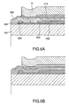
- Figs. 6A and 6B are cross-sectional views which illustrate the structure of the liquid discharge head manufactured by each of the processes represented in Figs. 5A to 5J: Fig. 6A shows the structure before the movable member and the electrode layer is separated; and Fig. 6B shows the structure after the movable member is separated from the electrode layer.
- bump holes 35 reaching the pedestal portion 7 are arranged on the movable member 31, and gold 212 is filled into the bump holes 35. In this manner, the movable member 31 and the pedestal portion 7 are bonded more strongly.
- nickel is used as the material of the movable member 31 in accordance with the present embodiment, but it may be possible to use gold or the like.
- the material of the grooved member 50 there are named Si, polysulfone, or the like, and as the material of the orifice plate 29, nickel, polyimide, or the like.
- the grooved member 50 is joined to the substrate 1 by the application of bonding agent or by use of spring.
- a liquid discharge head is completed through each processes of die bonding, TAB connection, incorporation of ink supply members, (bonding of the orifice plate), sealing, and (framing as required if plural heads are used, the incorporation of tank if the tank and head are formed together as one body, or the like).
- the substrates 1 and the grooved members 50 are formed on an Si wafer, it may be possible to bond them in the form of the wafer, and then, cut them into a chip mode, respectively.
- Figs. 9A to 9J are views which illustrate a method for manufacturing the liquid discharge head represented in Figs. 3A and 3B in accordance with a second embodiment of the present invention. The state of grooved film lamination is simplified.
- the electrode layer 210 formed by TiW layer or nickel layer is arranged by means of sputtering method or the like (Fig. 9B).
- the electrode layer 210 is coated by resist 211. After that, the resist 211 is patterned corresponding to the configuration of the pedestal portion 7 (Fig. 9C).
- the resist 211 is removed to make the pedestal portion 7 formed by gold 211 (Fig. 9E).
- the exfoliation layer 216 is formed in order to exfoliate the movable member 31 and the substrate 1 (Fig. 9F).
- the surface of the substrate 1 is coated with resist 214.
- the resist 214 is patterned corresponding to the configuration of the movable member 31 and the pedestal portion 7. In other words, the resist 214 on the area of the substrate 1 where the gold 212 and the exfoliation layer 216 are formed is removed (Fig. 9G).
- the surface of the substrate is electroformed using a material 217 having a high thermal expansion coefficient and a material 218 having a lower thermal expansion coefficient.
- the resist 214 has been patterned corresponding to the configuration of the movable member 31 and the pedestal portion 7 on the surface of the substrate, only the portion where the resist 214 has been removed by patterning is electroformed (Fig. 9H).
- the resist 214 is removed to form the movable member 31 provided with the supporting plate formed by the material 217 having the high thermal expansion coefficient and the material 218 having the low thermal expansion coefficient (Fig. 9I).
- the material 217 having the high thermal expansion coefficient and the material 218 having the low thermal expansion coefficient are curved by the application of heat.
- the movable member 31 and the electrode layer 210 are exfoliated (Fig. 9J).
- the uppermost layer of the surface of the substrate 1 is made electrode, there is no need for the production of the electrode layer 210.
- the material 217 having the high thermal expansion coefficient and the material 218 having the low thermal expansion coefficient that form the movable member 31 are curved depending on the temperature in the nozzle. In this manner, the gap between the movable member 31 and the heat generating member 2 is regulated. As a result, the characteristic changes caused by the temperatures in the nozzle can be controlled by changing the thermal expansion coefficients of the two kinds of materials that form the movable member 31.
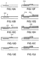
- Figs. 10A to 10J are views which illustrate a method for manufacturing the liquid discharge head represented in Figs. 3A and 3B in accordance with a third embodiment of the present invention. The state of the grooved film lamination is simplified.
- the electrode layer 210 formed by TiW layer or nickel layer is arranged by means of sputtering method or the like (Fig. 10B).
- the electrode layer 210 is coated by resist 211. After that, the resist 211 is patterned corresponding to the configuration of the pedestal portion 7 (Fig. 10C).
- the resist 211 is removed to make the pedestal portion 7 formed by gold 211 (Fig. 10E).
- the exfoliation layer 216 is formed in order to exfoliate the movable member 31 and the substrate 1 (Fig. 10F).
- the surface of the substrate 1 is coated with resist 214.
- the resist 214 is patterned corresponding to the configuration of the movable member 31 and the pedestal portion 7. In other words, the resist 214 on the area of the substrate 1 where the gold 212 and the exfoliation layer 216 are formed is removed (Fig. 10G).
- the surface of the substrate is electroformed using nickel 215.
- the resist 214 has been patterned corresponding to the configuration of the movable member 31 and the pedestal portion 7 on the surface of the substrate, only the portion where the resist 214 has been removed by patterning is electroformed with nickel 215 (Fig. 10H). Also, in this case, the stress moderator contained in the electroforming solution is adjusted so that the inner stress of nickel becomes tensile stress.
- the movable member 31 and the electrode layer 210 are exfoliated by the function of the exfoliation layer 216 and by means of the inner stress of the movable member 31, the electrode layer 210 and the movable member 31 are exfoliated to complete the liquid discharge head.
- the uppermost layer of the surface of the substrate 1 is made electrode, there is no need for the production of the electrode layer 210.
- the movable member 31 has a property that its leading end is curved upward with the pedestal portion 7 as the fulcrum thereof after the electrode layer 210 is exfoliated. Therefore, it becomes possible to secure the liquid generating area stably, and also, to move the movable member 31 efficiently at the time of foaming.
- Fig. 11 is a cross-sectional view which shows a liquid discharge head manufactured by the method for manufacturing liquid discharge heads in accordance with another embodiment of the present invention, taken in the liquid flow path.
- the present embodiment comprises the heat generating member 2 that creates bubbles by the application of heat; the substrate 1 on which the heat generating members 2 are incorporated; the discharge ports 18 for discharging liquid; the orifice plate 29 having the discharge ports 18 formed therefor to determine the discharge direction of liquid; liquid flow paths 10 for supplying the discharge liquid to each of the discharge ports 18; the grooved member 51 that forms each of the liquid flow paths 10, the movable member 31 displaceable along the creation of bubbles on each of the heat generating members 2; and the pedestal portions 7 that support the movable members 31, respectively.
- the groove walls that separate a plurality of liquid flow paths 10 from each other are arranged to extend in the direction toward the orifice plate 29, and formed integrally with the orifice plate 29.
- Figs. 12A to 12I are views which illustrate the method for manufacturing the liquid discharge head represented in Fig. 11 in accordance with one embodiment of the present invention.
- the electrode layer 210 formed by TiW layer or the like is arranged by means of sputtering method or the like (Fig. 12B).
- gold 212 is formed on the surface of the electrode layer 210 by means of sputtering method or the like (Fig. 12C).
- gold 212 is further electroformed on the surface of the substrate (Fig. 12D).
- the thickness of gold 212 is 0.5 to 10 ⁇ m.
- the surface of the substrate 1 is coated with resist 214.
- the resist 214 is patterned corresponding to the configuration of the movable member 31 and the pedestal portion 7 (Fig. 12E).
- nickel 215 the surface of the substrate is electroformed.
- the resist 214 has been patterned on the surface of the substrate corresponding to the configuration of the movable member 31 and the pedestal portion 7, nickel is electroformed only the portion where the resist 214 has been removed by patterning (Fig. 12F).
- the thickness of nickel 215 is 0.5 to 10 ⁇ m.
- gold 212 is removed by means of wet etching using potassium cyanide.
- the etching is terminated when all the gold has been removed by overetching under the movable portion of the movable member 31 (Fig. 12H).
- the electrode layer 210 is removed by means of etching using hydrogen peroxide (Fig. 12I).
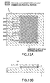
- Figs. 13A and 13B are views which illustrate the structure of the liquid discharge head manufactured by each of the processes represented in Figs. 12A to 12I; Fig. 13A is a plan view; Fig. 13B is a cross-sectional view.
- the formation step of the electrode layer 210 is not needed. Also, if the electro formation using gold is conducted directly on the tantalum layer 219 or the electrode layer 210, there is no need for the gold sputtering process, either.
- the present embodiment as described above makes it possible to control the gap between the movable member 31 and the heat generating member 2 more accurately by means of the pedestal portion 7.
- Figs. 14A to 14I are views which illustrate the method for manufacturing liquid discharge heads in accordance with a fifth embodiment of the present invention.
- lead 220 is formed by means of sputtering method or the like (Fig. 14B).
- lead 220 is removed by patterning (Fig. 14C).
- the electrode layer 210 is formed by means of sputtering method or the like on the surface of the substrate (Fig. 14D).
- the electrode 210 is patterned to remove the electrode layer 210 on the portion that becomes the pedestal of the movable member (Fig. 14E).
- the surface of the substrate 1 is coated with resist 214.
- the resist 214 is patterned corresponding to the configuration of the movable member and the pedestal portion (Fig. 14F).
- the surface of the substrate is electroformed.
- the resist 214 has been patterned on the surface of the substrate corresponding to the configuration of the movable member and the pedestal portion, nickel is electroformed only the portion where the resist 214 has been removed by patterning (Fig. 14G).
- the electrode layer 210 in the vicinity of the movable member is removed by means of etching (Fig. 14I).
- the recessed portion 221 is formed in the vicinity of the pedestal of the movable member. Therefore, the movable portion of the movable member is configured to be easily movable when liquid is discharged.
- Figs. 18A and 18B are views which illustrate the liquid discharge head manufactured by the method for manufacturing liquid discharge heads in accordance with one embodiment of the present invention
- Fig. 18A is a cross-section view
- Fig. 18B is a partially broken perspective view.
- the present embodiment comprises the heat generating member 2 that creates bubbles by the application of heat; the substrate 1 on which the heat generating members 2 are incorporated; the discharge ports 18 for discharging liquid; the orifice plate 29 having the discharge ports 18 formed therefor to determine the discharge direction of liquid; liquid flow paths 10 for supplying the discharge liquid to each of the discharge ports 18; the grooved member 51 that forms each of the liquid flow paths 10; and the movable member 31 displaceable along the creation of bubbles on each of the heat generating members 2.
- the groove walls 52 that separate a plurality of liquid flow paths 10 from each other are arranged to extend in the direction toward the orifice plate 29, and bonded to the orifice plate 29 by the application of bonding agent or the like.
- Figs. 19A to 19I are views which illustrate the method for manufacturing the liquid discharge head represented in Figs. 18A and 18B.
- the electrode layer 210 formed by TiW layer or nickel layer is arranged by means of sputtering method or the like (Fig. 19B).
- the electrode layer 210 is coated by resist 211. After that, the resist 211 on the position corresponding to the movable portion of the movable member is patterned (Fig. 19C).
- an organic conductive film 222 is coated by means of dipping or the like in order to enhance the releasability between the electrode layer and the electroformed nickel to be exercised later (Fig. 19D).
- the resist 211 is removed (Fig. 19E). Then, the configuration of the movable member and the non-movable area of the movable member are again patterned with resist. In this case, the non-movable area is of course made wider than the area where the releasing agent has been applied.
- the surface of the substrate 1 is coated with nickel 215 (Fig. 19G).
- the resist 214 is removed, and the movable member is formed with the supporting plate made of nickel 215 (Fig. 19H).
- the uppermost layer of the surface of the substrate 1 is made electrode, there is no need for the production of the electrode layer 210.
- Figs. 20A to 20I are views which illustrate each processing step of the method for manufacturing liquid discharge heads in accordance with the present embodiment. It is noted that each of processing steps shown in Fig. 20A to 20I corresponds to each of them in Fig. 19A to 19I.
- the amount of exposure is adjusted with respect to the resist 214 used for the electroformation of nickel serving as the movable member so as to make the thickness of the gap on the substrate 1 side in the thickness direction of the resist 214, while making it wider on the surface side.
- the exposure development is conducted (Fig. 20F).
- the nickel 215 on the area where the releasing agent has been applied and the substrate 1 are separated from each other by giving heat, ultrasonic waves or vibrations or these combined to the movable member made of the nickel 215 and the substrate 1 (Fig. 20I).
- Fig. 21 is a cross-sectional view which illustrates the fundamental structure of a liquid discharge head in accordance with the present invention, taken in the liquid flow direction.
- the liquid discharge head is provided with an elemental substrate 301 having a plurality of heat generating members 302 (in Fig. 21, only one is shown) arranged in series for giving thermal energy to create bubbles in liquid; a ceiling plate 303a to be bonded to the elemental substrate 301; and an orifice plate 304 joined to the front end of the elemental substrate 301 and the ceiling plate 303a.
- silicon oxide film or silicon nitride film is formed on a substrate made of silicon or the like for the purpose of insulation and heat accumulation. Then, patterning is given to it to provide the electric resistance layer and wiring for the formation of the heat generating member 302. When a voltage is applied to the electric resistance layer through the wiring, the electric current flows on the electric resistance layer to enable the heat generating member 302 to give heat.
- the ceiling plate 303a forms a plurality of liquid flow paths 307 corresponding to each of the heat generating members 302, and the common liquid chamber 308 for supplying liquid to each of the liquid flow paths 307 as well.
- the side walls 309 of liquid paths are integrally provided for the ceiling plate, which extend between the heat generating members 302, respectively.
- the ceiling plate 303a is formed by silicon material to make it possible to form the liquid flow paths 307 and the common liquid chamber 309 by etching the respective patterns or form them by etching the liquid flow paths 307 portion after material, such as silicon nitride or silicon oxide, is deposited on the silicon substrate by means of the known film formation method, such as the CVD, so as to make it the side walls of the flow paths.
- the orifice plate 304 On the orifice plate 304, a plurality of discharge ports 305 are formed, which are communicated with each of the liquid flow paths 307 and the common liquid chamber 305 through each of the liquid flow paths 307 correspondingly.
- the orifice plate 304 is also formed by silicon material.
- the orifice plate can be formed by cutting the silicon substrate having the discharge ports 305 formed therefor to a thickness of approximately 10 to 150 ⁇ m.
- the orifice plate 304 is not necessarily the constituent required for the structure of the present invention.
- the orifice plate 304 it may be possible to provide a ceiling plate with discharge ports by leaving a portion equivalent to the thickness of the orifice plate 304 intact on the wall of the leading end of the ceiling plate 303a when the liquid flow paths 307 are formed on the ceiling plate 303a, and then, the discharge ports 305 are formed on this particular portion thus left intact.
- a movable member 306 of cantilever type arranged to face the heat generating member 302 in order to separate the liquid flow paths 307 into first liquid flow paths 307a and the second liquid flow paths 307b in which each of the heat generating members 302 is arranged, respectively.
- the movable member 306 is a thin film formed by silicon material, such as silicon nitride or silicon oxide.
- the movable member 306 is arranged in a position to face the heat generating member 302 with a specific gap with it to cover the heat generating member 302 so that this member has the fulcrum 306a on the upstream side of the large flow made by the discharge operation of liquid from the common liquid chamber 308 to the discharge port 305 side through the movable member 306, and also, the free end 306b on the downstream side with respect to this fulcrum 306a.
- the pressure propagating direction of bubble is carried to the downstream side.
- the pressure of the bubble contributes directly to the discharge of liquid efficiently.
- the development direction of bubble itself is also carried to the downstream side as the propagating direction of the pressure so as to enable the bubble to be developed larger on the downstream side than the upstream side.
- the development direction of the bubble itself is controlled by means of the movable member, and the propagating direction of the bubble, as well. As a result, it becomes possible to enhance the fundamental discharge characteristics, such as the discharge efficiency and the discharge speeds, significantly.
- BPSG is formed on the substrate 201 by means of the CVD method at a temperature of 350°C (Fig. 23A).
- the film thickness of this BPSG is eventually equivalent to the gap between the movable portion of the movable member and the heat generating member, and such thickness is controlled to be at an optimal value between 1 ⁇ m and 20 ⁇ m where the movable member demonstrates its effect most remarkably in consideration of the entire balance of the flow paths.
- resist 203 is applied by means of spin coating or the like in order to pattern the BPSG (Fig. 23B), and then, exposed and developed (Fig. 23C), thus removing the resist on the portion corresponding to the fixed portion of the movable member.
- the BPSG having no resist thereon is removed by means of wet etching with buffered hydrofluoric acid. After that, the remaining resist is removed by applying to it the plasma ashing using oxygen plasma or by dipping it in the resist removal solution (Fig. 23E).
- SiN film is formed on the BPSG in a thickness of 1 to 10 ⁇ m (here, the best composition of the SiN film is Si 3 N 4 , but there is no problem if N is in a range of 1 to 1.5 with respect to the Si : 1 to obtain the anticipated effect of the movable member) by the performance of plasma CVD with ammonia and silane gas at a temperature of 400°C.
- the SiN film is generally used for the semiconductor process, and this film has resistance to alkali and presents chemical stability, and also, it has resistance to ink.
- this film becomes the movable member ultimately, there is no particular restriction on the method of manufacture whereby to attain the composition and structure in order to obtain the optimal value of material.
- the formation method of SiN it is possible to adopt not only the plasma CVD as described earlier, but also, to use the atmospheric CVD, LP (low pressure) CVD, biased ECRCVD, microwave CVD, or sputtering or coating for its formation.
- the composition factors of the SiN film step by step may be changed to make it a multi-layered film in order to enhance its stress, rigidity, Young's modulus, and other physical properties, as well as resistance to alkali, acid resistance, and other chemical properties, or the film is made multi-layered by adding impurities step by step or it may be possible to add impurities to a single layer.
- resist is applied by spin coating in order to pattern the SiN film. After patterning, the configuration of the movable member is etched by dry etching, reactive ion etching, or the like using CF 4 gas or the like.
- the SiO film may be adoptable if it is easily etched at a lower temperature, such as 400°C or less or it may be possible to use PSG with only P being added. Also, besides those mentioned above, it may be possible to use an organic material from the viewpoint of easier process.
- the thickness of the movable member is regulated to be 1 to 10 ⁇ m as described above.
- the relative thickness of the SiN is made 1/2 of the Ni of the movable member which is known publicly, for example, because its Young's modulus is higher approximately two times.
- the above description has been made only of the movable member, but the supporting portion of the movable member may be made together at a time, but the effect of the present invention is not affected at all, either, even if the supporting portion is formed by different material in order to make its close contact or the method of manufacture simpler.
- the movable member may be formed with diamond film or amorphous carbon hydride film.
- the diamond film thus formed is excellent in its physical properties (for example, its Young's modulus is approximately three times SiN, and relatively, the same effect is still obtainable in a thickness of 1/3). Its chemical stability is also high, while having an excellent heat radiation. Therefore, this film is more suitable for the movable member than SiN film. Also, the amorphous carbon hydride film is better than the SiN film, although it is inferior to the diamond film in the physical properties. Consequently, from the viewpoint of the balance in costs of manufacture, that is, performance and difficulty in its manufacture, the amorphous carbon hydride film is also usable in place of the diamond film or the SiN film.
- the same effect is obtainable with the movable member being formed by SiC.
- the same effect is still obtainable by C being in a range of 0.5 to 1.5.
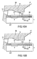
- Figs. 15A and 15B are vertically sectional views which illustrate one structural example of the liquid jet apparatus to which the liquid discharge head of the present invention is applicable; Fig. 15A shows the apparatus having a protection film to be described later; and Fig. 15B shows the apparatus which is not provided any protection film.
- the liquid flow path designated by a reference numeral 10 in Figs. 1A to 1D is designated as the first liquid flow path 14.
- the liquid supply path designated by a reference numeral 12 is designated as the second liquid flow path 16. It may be possible to supply the same liquid to each of the liquid flow paths, but if different liquids may be made usable, the selection range becomes wider for the liquids to be supplied to the first liquid flow path, that is, such range is made wider for the selection of discharge liquids.
- a grooved member 50 having grooves that constitute the second liquid flow path 16, separation walls 30, movable member 31, and first liquid flow path 14.
- a silicon oxide film or a silicon nitride film 106 is formed on the substrate 107 of silicon or the like for the purpose of insulation and heat accumulation.
- an electric resistance layer 105 of hafnium boride (HfB 2 ), tantalum nitride (TaN), tantalum aluminum (TaAl) or the like which forms a heat generating member in a thickness of 0.01 to 0.2 ⁇ m, and wiring electrodes 104 of aluminum or the like in a thickness of 0.2 to 1.0 ⁇ m.
- a voltage is applied to the electric resistance layer 105 from the two wiring electrodes 104 to cause electric current to run for generating heat.
- a protection layer 103 of silicon oxide, silicon nitride, or the like is formed in a thickness of 0.1 to 0.2 ⁇ m. Further on it, an anti-cavitation layer 102 of tantalum or the like is formed in a thickness of 0.1 to 0.6 ⁇ m, hence protecting the electric resistance layer 105 from ink or various other kinds of liquids.
- the pressure and shock waves are extremely strong, particularly when each of the bubbles is foamed or defoamed.
- an alloy of iridium-tantalum-aluminum is adoptable. Now that the present invention makes it possible to separate the liquid for foaming use from the discharge liquid, it presents its particular advantage when no protection layer is adopted in a case like this.
- the structure of the heat generating member 2 adopted for the present embodiment may be provided only with the electric resistance layer 105 (heat generating portion) across the wiring electrodes 104 or may be arranged to include a protection layer to protect the electric resistance layer.
- the heat generating member 2 which is adopted therefor, is provided with the heat generating portion formed by the resistance layer that generates heat in accordance with electric signals.
- the present invention is not necessarily limited to such device. It should be good enough if only the device can create each bubble in the foam liquid, which is capable enough to discharge the liquid for discharging use.
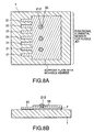
- the elemental substrate 1 described earlier there may be incorporated functional devices integrally by the semiconductor manufacturing processes, such as transistors, didoes, latches, shift registers, which are needed for selectively driving the electrothermal transducing devices, besides each of the electrothermal transducing devices, which is structured by the electric resistance layer 105 that forms the heat generating portion, and wiring electrodes 104 that supply electric signals to the electric resistance layer 105.
- functional devices integrally by the semiconductor manufacturing processes such as transistors, didoes, latches, shift registers, which are needed for selectively driving the electrothermal transducing devices, besides each of the electrothermal transducing devices, which is structured by the electric resistance layer 105 that forms the heat generating portion, and wiring electrodes 104 that supply electric signals to the electric resistance layer 105.
- each electrothermal transducing device arranged on the elemental substrate 1 described above so as to apply rectangular pulses to the electric resistance layer 105 through the wiring electrodes 104 to cause the layer between the electrodes to generate heat abruptly for discharging liquid.
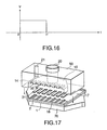
- Fig. 16 is a view which shows the voltage waveform to be applied to the electric resistance layer 105 represented in Figs. 15A and 15B.
- the electric signal of 6 kHz is applied at a voltage 24V with the pulse width of 7 ⁇ sec, and at the electric current of 150 mA to drive each heat generating member.
- ink serving as liquid is discharged from each of the discharge ports.
- the present invention is not necessarily limited to these conditions of driving signal. It may be possible to apply the driving signals under any condition if only such signals can act upon the foam liquid to foam appropriately.
- Fig. 17 is an exploded perspective view which shows one structural example of the liquid jet apparatus to which the liquid discharge head of the present invention is applicable.
- an elemental substrate 1 is arranged on a supporting member 70 made of aluminum or other metal.
- a plurality of electrothermal transducing devices serving as the heat generating members 2 are arranged for generating heat to create bubbles by means of film boiling in foaming liquid.
- a plurality of grooves formed by DF dry film which constitute the second liquid flow paths 16; a recessed portion communicated with the plural second liquid flow paths 16 and forms a second common liquid chamber (common foaming liquid chamber) 17 to supply foaming liquid to each of the second liquid flow paths 16; and the separation walls 30 having the movable members 31 bonded thereto as described earlier.
- the grooved member 50 is provided with grooves that constitute first liquid flow paths (discharge liquid flow paths) 14 when it is bonded to the separation walls 30; a recessed portion that forms the first common liquid chamber (common discharge liquid chamber) 15 to supply discharge liquid to each of the first liquid flow paths 14; the first liquid supply path (discharge liquid supply path) 20 to supply discharge liquid to the first common liquid chamber 15; and the second liquid supply path (foaming liquid supply path) 21 to supply foaming liquid to the second common liquid chamber 17.
- the second liquid supply path 21 penetrates the movable members 31 arranged outside the first common liquid chamber 15 and the separation walls 30 to be connected with the conductive path which is communicated with the second common liquid chamber 17. Through this conductive path, the foaming liquid is supplied to the second common liquid chamber 17 without being mixed with the discharge liquid.
- the arrangement relationship between the elemental substrate 1, movable members 31, separation walls 30, and grooved member 50 is such that the movable members 31 are arranged corresponding to the heat generating members 2 on the elemental substrate 1, and then, the first liquid flow paths 14 are arranged corresponding to the movable members 31.
- the sectional areas of the first liquid supply path 20 and second liquid supply path 21 may be determined in proportion to the amount of supplies. To optimize the sectional areas of liquid flow paths makes it possible to implement making the parts that constitute the grooved member 50 and others smaller still.
- each movable member is separated from the substrate after each movable member is formed on it.
- the movable members are incorporated in a liquid discharge head.
- the movable members are incorporated on the substrate formed by a material having resistance to ink. Therefore, not only the movable members that face each of the bubble generating areas are utilized for discharging liquid by guiding bubbles created on the bubble generating area efficiently, but also, the movable members can be manufactured easily. Thus, it is possible to provide a highly reliable liquid discharge head and the substrate for use of such liquid discharge head as well.
- a method for manufacturing liquid discharge heads is provided with discharge ports for discharging liquid, liquid flow paths communicated with the discharge ports for supplying liquid to the discharge ports, a substrate having heat generating members for creating bubbles in liquid, and movable members facing the heat generating members, each being arranged in each liquid flow path, having the free end on the discharge port side with a specific gap with the heat generating member.
- This method comprises the steps of forming the boundary layer used for providing a gap between the movable member and the substrate above the heat generating member on the substrate, of laminating the movable member on the boundary layer so as to position the free end above the heat generating member, at the same time fixing the movable member on the substrate, and of forming the gap between the movable member and the heat generating member by use of the boundary layer.
Landscapes
- Engineering & Computer Science (AREA)
- Manufacturing & Machinery (AREA)
- Particle Formation And Scattering Control In Inkjet Printers (AREA)
Claims (21)
- Procédé pour la fabrication d'une tête à décharge de liquide pourvue :d'orifices (18) de décharge destinés à décharger un liquide ;de trajets (10) d'écoulement de liquide communiquant avec lesdits orifices de décharge pour alimenter en liquide lesdits orifices de décharge ;d'un substrat (1 ; 201) comportant des éléments (2) de génération de chaleur destinés à créer une bulle dans un liquide ; etd'un élément mobile (31) agencé dans chacun desdits trajets (10) d'écoulement de liquide, ledit élément mobile (31) faisant face à l'un, associé, desdits éléments (2) de génération de chaleur et ayant une extrémité libre du côté dudit orifice de décharge avec un intervalle spécifique entre ledit élément mobile (31) et ledit substrat (1 ; 201) au-dessus dudit élément associé (2) de génération de chaleur, caractérisé en ce que le procédé comprend les étapes qui consistent :à former une couche limite (210 ; 210, 212 ; 213 ; 216 ; 222) utilisée pour établir ledit intervalle sur ledit substrat (1 ; 201) ;à stratifier ledit élément mobile (31) sur ladite couche limite (210 ; 210, 212 ; 213 ; 216 ; 222) afin de positionner ladite extrémité libre au-dessus dudit élément associé (2) de génération de chaleur et de fixer ledit élément mobile sur ledit substrat (1 ; 201) ; età former ledit intervalle entre ledit élément mobile (31) et ledit substrat (1 ; 201) en utilisant ladite couche limite (210 ; 210, 212 ; 213 ; 216, 222).
- Procédé selon la revendication 1, dans lequel ladite couche limite est pourvue d'une couche anti-adhérente (216) n'ayant pas un pouvoir d'adhésion supérieur avec ledit élément mobile (31), et ledit élément mobile (31) est séparé de ladite couche anti-adhérente (216) par la contrainte exercée par ledit élément mobile (31) pour la formation dudit intervalle.
- Procédé selon la revendication 1, dans lequel ladite couche limite est formée par une matière (210 : 210, 212 ; 213) pouvant être enlevée sélectivement par rapport audit élément mobile (31), et ledit intervalle est formé par l'enlèvement de la couche limite se trouvant au-dessus dudit élément associé (2) de génération de chaleur.
- Procédé selon la revendication 1, dans lequel ledit élément mobile (31) est fixé audit substrat (1) au moyen d'une partie d'embase (7) située sur ledit substrat (1).
- Procédé selon la revendication 4, dans lequel ledit élément mobile (31) est fixé audit substrat (1) par liaison dudit élément mobile (31) et de ladite partie d'embase (7).
- Procédé selon la revendication 3, dans lequel ladite couche limite est formée par une couche de matière fusible (213), et ladite couche limite est chauffée de façon à fondre pour l'enlèvement de la couche limite.
- Procédé selon la revendication 1, dans lequel ledit élément mobile (31) est formé par électroformation sur ledit substrat (1).
- Procédé selon la revendication 7, dans lequel ladite couche limite (210 ; 210, 212) est formée d'une matière conductrice.
- Procédé selon la revendication 4, dans lequel ledit élément mobile (31) est relié au substrat (1) par l'intermédiaire de ladite couche limite (210, 212) et la partie restante de la couche limite (210, 212) après l'enlèvement devient ladite partie d'embase (7).
- Procédé selon la revendication 3, dans lequel ladite étape de formation dudit élément mobile est réalisée par la formation d'un motif après que la couche de matière (204) devenant l'élément mobile a été appliquée par pelliculage sur ledit substrat (201).
- Procédé selon la revendication 1, dans lequel ledit élément mobile (31) est fixé audit substrat (1) par stratification de l'élément mobile (31) sur une partie dudit substrat (1) mise à découvert de ladite couche limite (222).
- Procédé selon la revendication 1, dans lequel ledit élément mobile (31) est formé d'un métal.
- Procédé selon la revendication 12, dans lequel ledit métal est de l'or ou du nickel.
- Procédé selon la revendication 4, dans lequel ladite partie d'embase (7) est formée d'un métal.
- Procédé selon la revendication 14, dans lequel ledit métal est du plomb ou de l'or.
- Procédé selon la revendication 10, dans lequel ladite couche de matière (204) devenant ledit élément mobile (31) est formée de l'un du nitrure de silicium, du diamant, de l'hydrure de carbone amorphe et du carbure de silicium.
- Procédé selon la revendication 1, dans lequel ladite couche limite est une couche anti-adhérente (222) n'ayant pas un pouvoir d'adhésion supérieur avec ledit élément mobile (31), et ledit élément mobile (31) est séparé de ladite couche anti-adhérente (222) par l'application d'un chauffage, d'ondes ultrasonores ou de vibrations ou de plusieurs d'entre eux pour former ledit intervalle.
- Procédé selon la revendication 1, dans lequel l'aire de la surface dudit élément mobile est formée de façon à être plus grande sur le côté opposé dudit élément mobile que l'aire de la surface sur le côté dudit élément mobile tourné vers ledit élément de génération de chaleur.
- Tête à décharge de liquide, comportant :caractérisée en ce qu'une couche anti-adhérente (222) est disposée sur le substrat (1) et entre la partie extrême libre (32) dudit élément mobile (31) et le substrat, etune pluralité d'orifices de décharge (18) destinés à décharger un liquide ;une pluralité de trajets (10) d'écoulement de liquide communiquant avec chacun desdits orifices de décharge pour alimenter en liquide chacun desdits orifices de décharge ;un substrat (1) pourvu d'éléments (2) de génération de chaleur pour créer une bulle dans un liquide ;un élément mobile (31) agencé dans chacun de ladite pluralité de trajets (10) d'écoulement de liquide, l'élément mobile ayant une partie extrême libre (32) du côté dudit orifice de décharge destinée à faire face à l'un, associé, desdits éléments (2) de génération de chaleur ; etune partie d'embase (7) formée sur ledit substrat pour supporter ledit élément mobile (31),
en ce que ledit élément mobile (31) a pour propriété d'être courbé par la chaleur afin que la partie extrême libre (32) se sépare de la couche anti-adhérente (222) dans les conditions de température prévalant dans la tête à décharge de liquide pendant son fonctionnement. - Tête à décharge de liquide, comportant :caractérisée en ce qu'une couche anti-adhérente (216) est disposée sur le substrat (1) et entre la partie extrême libre (32) dudit élément mobile (31) et le substrat, etune pluralité d'orifices (18) de décharge destinés à décharger un liquide ;une pluralité de trajets (10) d'écoulement de liquide communiquant avec chacun desdits orifices de décharge pour alimenter en liquide chacun desdits orifices de décharge ;un substrat (1) pourvu d'éléments (2) de génération de chaleur destinés à créer une bulle dans un liquide ;un élément mobile (31) agencé dans chacun de ladite pluralité de trajets (10) d'écoulement de liquide, l'élément mobile ayant une partie extrême libre du côté dudit orifice de décharge, destinée à faire face à l'un, associé, desdits éléments (2) de génération de chaleur ; etune partie d'embase (7) formée sur ledit substrat (1) pour supporter ledit élément mobile (31),
en ce que l'élément mobile (31) a pour propriété d'être courbé par une contrainte intérieure de l'élément mobile afin que la partie extrême libre (32) soit séparée de la couche anti-adhérente (216). - Tête à décharge de liquide selon la revendication 19 ou 20,
dans laquelle la partie extrême libre dudit élément mobile (31) est pourvue d'une portion évidée sur la partie adjacente à ladite partie d'embase (7).
Applications Claiming Priority (6)
| Application Number | Priority Date | Filing Date | Title |
|---|---|---|---|
| JP21083197 | 1997-08-05 | ||
| JP21083197A JPH1148488A (ja) | 1997-08-05 | 1997-08-05 | 液体吐出ヘッドの製造方法及び液体吐出ヘッド |
| JP210831/97 | 1997-08-05 | ||
| JP336060/97 | 1997-12-05 | ||
| JP33606097A JP3639707B2 (ja) | 1997-12-05 | 1997-12-05 | 液体吐出ヘッド及びヘッド用基板 |
| JP33606097 | 1997-12-05 |
Publications (2)
| Publication Number | Publication Date |
|---|---|
| EP0895861A1 EP0895861A1 (fr) | 1999-02-10 |
| EP0895861B1 true EP0895861B1 (fr) | 2003-11-26 |
Family
ID=26518294
Family Applications (1)
| Application Number | Title | Priority Date | Filing Date |
|---|---|---|---|
| EP98114671A Expired - Lifetime EP0895861B1 (fr) | 1997-08-05 | 1998-08-04 | Tête d'ejection de liquide, substrat et methode de fabrication |
Country Status (3)
| Country | Link |
|---|---|
| US (2) | US6374482B1 (fr) |
| EP (1) | EP0895861B1 (fr) |
| DE (1) | DE69819976T2 (fr) |
Families Citing this family (28)
| Publication number | Priority date | Publication date | Assignee | Title |
|---|---|---|---|---|
| JP3524340B2 (ja) * | 1997-08-26 | 2004-05-10 | キヤノン株式会社 | 液体吐出ヘッド |
| US6391527B2 (en) * | 1998-04-16 | 2002-05-21 | Canon Kabushiki Kaisha | Method of producing micro structure, method of production liquid discharge head |
| US6918655B2 (en) * | 1998-10-16 | 2005-07-19 | Silverbrook Research Pty Ltd | Ink jet printhead with nozzles |
| EP1121249B1 (fr) * | 1998-10-16 | 2007-07-25 | Silverbrook Research Pty. Limited | Procede de fabrication d'une buse pour une tete d'impression a jet d'encre |
| JP3907329B2 (ja) * | 1998-12-03 | 2007-04-18 | キヤノン株式会社 | 液体吐出ヘッドおよび液体吐出装置 |
| JP3762172B2 (ja) * | 1998-12-03 | 2006-04-05 | キヤノン株式会社 | 液体吐出ヘッド、該液体吐出ヘッドが搭載されたヘッドカートリッジと液体吐出装置、及び該液体吐出ヘッドの製造方法 |
| WO2000071345A1 (fr) * | 1999-05-24 | 2000-11-30 | Matsushita Electric Industrial Co. Ltd. | Tete a jet d'encre et son procede de production |
| US6591500B1 (en) | 1999-06-04 | 2003-07-15 | Canon Kabushiki Kaisha | Method of manufacturing a liquid discharge head |
| JP3548536B2 (ja) * | 2000-02-15 | 2004-07-28 | キヤノン株式会社 | 液体吐出ヘッドの製造方法 |
| US6474792B2 (en) | 2000-07-31 | 2002-11-05 | Canon Kabushiki Kaisha | Liquid discharge head, method for manufacturing liquid discharge head, head cartridge on which liquid discharge head is mounted, and liquid discharge apparatus |
| US6834423B2 (en) * | 2000-07-31 | 2004-12-28 | Canon Kabushiki Kaisha | Method of manufacturing a liquid discharge head |
| JP4532785B2 (ja) | 2001-07-11 | 2010-08-25 | キヤノン株式会社 | 構造体の製造方法、および液体吐出ヘッドの製造方法 |
| JP4095368B2 (ja) * | 2001-08-10 | 2008-06-04 | キヤノン株式会社 | インクジェット記録ヘッドの作成方法 |
| JP3970119B2 (ja) * | 2002-07-19 | 2007-09-05 | キヤノン株式会社 | インクジェット記録ヘッドおよび該インクジェット記録ヘッドを用いた記録装置 |
| DE602005022448D1 (de) * | 2004-06-28 | 2010-09-02 | Canon Kk | Ekopfs und unter verwendung dieses verfahrens erhaltener flüssigkeitsausgabekopf |
| JP4208793B2 (ja) * | 2004-08-16 | 2009-01-14 | キヤノン株式会社 | インクジェットヘッド用基板、該基板の製造方法および前記基板を用いるインクジェットヘッド |
| JP4208794B2 (ja) * | 2004-08-16 | 2009-01-14 | キヤノン株式会社 | インクジェットヘッド用基板、該基板の製造方法および前記基板を用いるインクジェットヘッド |
| WO2006051762A1 (fr) * | 2004-11-10 | 2006-05-18 | Canon Kabushiki Kaisha | Tête de décharge liquide |
| JP4459037B2 (ja) * | 2004-12-01 | 2010-04-28 | キヤノン株式会社 | 液体吐出ヘッド |
| JP2007230194A (ja) | 2006-03-03 | 2007-09-13 | Canon Finetech Inc | インクジェット記録ヘッドおよび製造方法 |
| JP2007230193A (ja) * | 2006-03-03 | 2007-09-13 | Canon Finetech Inc | 液体吐出ヘッド |
| US7456548B2 (en) * | 2006-05-09 | 2008-11-25 | Canon Kabushiki Kaisha | Piezoelectric element, piezoelectric actuator, and ink jet recording head |
| US8034724B2 (en) | 2006-07-21 | 2011-10-11 | Semiconductor Energy Laboratory Co., Ltd. | Method for manufacturing semiconductor device |
| JP4290211B2 (ja) * | 2006-08-11 | 2009-07-01 | キヤノン株式会社 | 結晶性金属膜 |
| JP4221611B2 (ja) * | 2006-10-31 | 2009-02-12 | セイコーエプソン株式会社 | 液体噴射ヘッドの製造方法 |
| US7811911B2 (en) | 2006-11-07 | 2010-10-12 | Semiconductor Energy Laboratory Co., Ltd. | Method for manufacturing semiconductor device |
| JP5046819B2 (ja) | 2007-09-13 | 2012-10-10 | キヤノン株式会社 | スルーホールの形成方法およびインクジェットヘッド |
| US8566943B2 (en) * | 2009-10-01 | 2013-10-22 | Kaspersky Lab, Zao | Asynchronous processing of events for malware detection |
Family Cites Families (37)
| Publication number | Priority date | Publication date | Assignee | Title |
|---|---|---|---|---|
| CA1127227A (fr) | 1977-10-03 | 1982-07-06 | Ichiro Endo | Procede d'enregistrement a jet liquide et appareil d'enregistrement |
| US4611219A (en) | 1981-12-29 | 1986-09-09 | Canon Kabushiki Kaisha | Liquid-jetting head |
| US4881318A (en) | 1984-06-11 | 1989-11-21 | Canon Kabushiki Kaisha | Method of manufacturing a liquid jet recording head |
| JPS6159911A (ja) | 1984-08-30 | 1986-03-27 | Nec Corp | 切換スイツチ回路 |
| JPS6159914A (ja) | 1984-08-31 | 1986-03-27 | Fujitsu Ltd | デイジタル圧縮装置 |
| US4592414A (en) | 1985-03-06 | 1986-06-03 | Mccord Heat Transfer Corporation | Heat exchanger core construction utilizing a plate member adaptable for producing either a single or double pass flow arrangement |
| DE3514550A1 (de) | 1985-04-23 | 1986-10-23 | Hüls AG, 4370 Marl | 3-hydroxydicarbonsaeuren und ein verfahren zu ihrer herstellung |
| US4860033A (en) | 1987-02-04 | 1989-08-22 | Canon Kabushiki Kaisha | Base plate having an oxidation film and an insulating film for ink jet recording head and ink jet recording head using said base plate |
| JPS63197652A (ja) * | 1987-02-13 | 1988-08-16 | Canon Inc | インクジエツト記録ヘツドおよびその製造方法 |
| JPS63199972A (ja) | 1987-02-13 | 1988-08-18 | Canon Inc | 弁素子の製造方法 |
| US4994825A (en) | 1988-06-30 | 1991-02-19 | Canon Kabushiki Kaisha | Ink jet recording head equipped with a discharging opening forming member including a protruding portion and a recessed portion |
| US5081474A (en) | 1988-07-04 | 1992-01-14 | Canon Kabushiki Kaisha | Recording head having multi-layer matrix wiring |
| US5208604A (en) | 1988-10-31 | 1993-05-04 | Canon Kabushiki Kaisha | Ink jet head and manufacturing method thereof, and ink jet apparatus with ink jet head |
| GB8921722D0 (en) * | 1989-09-26 | 1989-11-08 | British Telecomm | Micromechanical switch |
| US5135605A (en) * | 1991-04-29 | 1992-08-04 | At&T Bell Laboratories | Methods for making mirrors |
| US5479197A (en) | 1991-07-11 | 1995-12-26 | Canon Kabushiki Kaisha | Head for recording apparatus |
| JPH05124189A (ja) * | 1991-11-01 | 1993-05-21 | Matsushita Electric Ind Co Ltd | インク吐出装置 |
| US5278585A (en) * | 1992-05-28 | 1994-01-11 | Xerox Corporation | Ink jet printhead with ink flow directing valves |
| JP3475512B2 (ja) | 1994-04-22 | 2003-12-08 | 日産自動車株式会社 | ロックアップ装置の油圧回路 |
| AU4092296A (en) | 1995-01-13 | 1996-08-08 | Canon Kabushiki Kaisha | Liquid ejecting head, liquid ejecting device and liquid ejecting method |
| TW332799B (en) | 1995-01-13 | 1998-06-01 | Canon Kk | The liquid ejecting head, device and method of liquid ejecting |
| AU4092396A (en) | 1995-01-13 | 1996-08-08 | Canon Kabushiki Kaisha | Liquid ejecting head, liquid ejecting device and liquid ejecting method |
| JP3342279B2 (ja) | 1995-01-13 | 2002-11-05 | キヤノン株式会社 | 液体吐出方法、液体吐出ヘッドおよび該液体吐出ヘッドの製造方法 |
| JP3706671B2 (ja) | 1995-04-14 | 2005-10-12 | キヤノン株式会社 | 液体吐出ヘッド、液体吐出ヘッドを用いたヘッドカートリッジ、液体吐出装置、および液体吐出方法 |
| KR100230162B1 (ko) * | 1995-04-14 | 1999-11-15 | 미따라이 후지오 | 액체 토출 헤드 및 그 제조 방법 |
| CA2175166C (fr) | 1995-04-26 | 2000-08-08 | Toshio Kashino | Tete d'ejection de liquide, dispositif et methode connexe |
| US5838351A (en) | 1995-10-26 | 1998-11-17 | Hewlett-Packard Company | Valve assembly for controlling fluid flow within an ink-jet pen |
| US6213592B1 (en) | 1996-06-07 | 2001-04-10 | Canon Kabushiki Kaisha | Method for discharging ink from a liquid jet recording head having a fluid resistance element with a movable member, and head, head cartridge and recording apparatus using that method |
| JP3647205B2 (ja) | 1996-06-07 | 2005-05-11 | キヤノン株式会社 | 液体吐出方法、液供給方法、液体吐出ヘッド、該液体吐出ヘッドを用いた液体吐出ヘッドカートリッジ、及び液体吐出装置 |
| US5872582A (en) * | 1996-07-02 | 1999-02-16 | Hewlett-Packard Company | Microfluid valve for modulating fluid flow within an ink-jet printer |
| JP3403008B2 (ja) | 1996-07-05 | 2003-05-06 | キヤノン株式会社 | 液体吐出ヘッドおよびそれを用いたヘッドカートリッジと記録装置 |
| JP3408066B2 (ja) | 1996-07-09 | 2003-05-19 | キヤノン株式会社 | 液体吐出ヘッド、液体吐出ヘッドを用いたヘッドカートリッジ、液体吐出装置、液体吐出方法およびヘッドキット |
| JP3372765B2 (ja) | 1996-07-12 | 2003-02-04 | キヤノン株式会社 | 液体吐出ヘッド、ヘッドカートリッジ、液体吐出装置、記録システム、ヘッドキット、および液体吐出ヘッドの製造方法 |
| JP3403009B2 (ja) | 1996-07-12 | 2003-05-06 | キヤノン株式会社 | 可動部材の変位と気泡成長を伴う液体吐出方法、該吐出方法に用いられる液体吐出ヘッド、ヘッドカートリッジ及びこれらを用いた液体吐出装置 |
| JP3524340B2 (ja) | 1997-08-26 | 2004-05-10 | キヤノン株式会社 | 液体吐出ヘッド |
| DE69813154T2 (de) * | 1997-12-05 | 2004-03-04 | Canon K.K. | Flüssigkeitsausstosskopf, Flüssigkeitsausstossverfahren, Kopfkassette und Flüssigkeitsausstossvorrichtung |
| JP2000198199A (ja) * | 1997-12-05 | 2000-07-18 | Canon Inc | 液体吐出ヘッドおよびヘッドカートリッジおよび液体吐出装置および液体吐出ヘッドの製造方法 |
-
1998
- 1998-08-04 EP EP98114671A patent/EP0895861B1/fr not_active Expired - Lifetime
- 1998-08-04 US US09/128,538 patent/US6374482B1/en not_active Expired - Fee Related
- 1998-08-04 DE DE69819976T patent/DE69819976T2/de not_active Expired - Lifetime
-
2002
- 2002-02-11 US US10/071,799 patent/US6834943B2/en not_active Expired - Fee Related
Also Published As
| Publication number | Publication date |
|---|---|
| US6834943B2 (en) | 2004-12-28 |
| US6374482B1 (en) | 2002-04-23 |
| US20020093553A1 (en) | 2002-07-18 |
| DE69819976T2 (de) | 2004-09-02 |
| EP0895861A1 (fr) | 1999-02-10 |
| DE69819976D1 (de) | 2004-01-08 |
Similar Documents
| Publication | Publication Date | Title |
|---|---|---|
| EP0895861B1 (fr) | Tête d'ejection de liquide, substrat et methode de fabrication | |
| KR100337847B1 (ko) | 액체 토출 헤드 및 액체 토출 방법 | |
| US6485132B1 (en) | Liquid discharge head, recording apparatus, and method for manufacturing liquid discharge heads | |
| US6386686B1 (en) | Liquid discharge head, manufacturing method of liquid discharge head, head cartridge, and liquid discharge apparatus | |
| KR100312948B1 (ko) | 액체토출방법및액체토출헤드 | |
| KR100395529B1 (ko) | 잉크젯 프린트 헤드 및 그 제조방법 | |
| KR100388180B1 (ko) | 액체 토출 헤드의 제조 방법 | |
| EP0899104B1 (fr) | Tête d'éjection de liquide et sa méthode de fabrication | |
| US9393781B2 (en) | Liquid-discharging head and method of producing the same | |
| EP1005995A2 (fr) | Procédé de fabrication d'une tête à jet de liquide, tête à jet de liquide, cartouche et appareil d'enregistrement à jet de liquide | |
| JP3266582B2 (ja) | 形状記憶合金を利用したプリンタヘッド及びその製造方法 | |
| KR100413680B1 (ko) | 버블 젯 방식의 잉크 젯 프린트 헤드 | |
| JP2003118114A (ja) | インクジェットヘッド及びその製造方法 | |
| JPH1148488A (ja) | 液体吐出ヘッドの製造方法及び液体吐出ヘッド | |
| JP3639707B2 (ja) | 液体吐出ヘッド及びヘッド用基板 | |
| JPH05220960A (ja) | 液体噴射記録ヘッド | |
| JP3592108B2 (ja) | 液体吐出ヘッド、液体吐出装置および液体吐出方法 | |
| JP3554149B2 (ja) | 液体吐出ヘッドの製造方法 | |
| JPH11170532A (ja) | 液体噴射記録ヘッド | |
| JP4489637B2 (ja) | インクジェットヘッドおよびその製造方法 | |
| KR100374591B1 (ko) | 형상기억합금을 이용한 프린터 헤드 및 그 제조방법 | |
| JP3347590B2 (ja) | 液体吐出ヘッド、ヘッドカートリッジ及び液体吐出装置 | |
| JP3706774B2 (ja) | 液体吐出ヘッドおよび液体吐出方法 | |
| JPH06320730A (ja) | サーマルインクジェットヘッド |
Legal Events
| Date | Code | Title | Description |
|---|---|---|---|
| PUAI | Public reference made under article 153(3) epc to a published international application that has entered the european phase |
Free format text: ORIGINAL CODE: 0009012 |
|
| AK | Designated contracting states |
Kind code of ref document: A1 Designated state(s): CH DE ES FR GB IT LI NL SE |
|
| AX | Request for extension of the european patent |
Free format text: AL;LT;LV;MK;RO;SI |
|
| 17P | Request for examination filed |
Effective date: 19990706 |
|
| AKX | Designation fees paid |
Free format text: CH DE ES FR GB IT LI NL SE |
|
| 17Q | First examination report despatched |
Effective date: 20010129 |
|
| GRAH | Despatch of communication of intention to grant a patent |
Free format text: ORIGINAL CODE: EPIDOS IGRA |
|
| GRAH | Despatch of communication of intention to grant a patent |
Free format text: ORIGINAL CODE: EPIDOS IGRA |
|
| GRAA | (expected) grant |
Free format text: ORIGINAL CODE: 0009210 |
|
| AK | Designated contracting states |
Kind code of ref document: B1 Designated state(s): CH DE ES FR GB IT LI NL SE |
|
| PG25 | Lapsed in a contracting state [announced via postgrant information from national office to epo] |
Ref country code: NL Free format text: LAPSE BECAUSE OF FAILURE TO SUBMIT A TRANSLATION OF THE DESCRIPTION OR TO PAY THE FEE WITHIN THE PRESCRIBED TIME-LIMIT Effective date: 20031126 Ref country code: LI Free format text: LAPSE BECAUSE OF FAILURE TO SUBMIT A TRANSLATION OF THE DESCRIPTION OR TO PAY THE FEE WITHIN THE PRESCRIBED TIME-LIMIT Effective date: 20031126 Ref country code: CH Free format text: LAPSE BECAUSE OF FAILURE TO SUBMIT A TRANSLATION OF THE DESCRIPTION OR TO PAY THE FEE WITHIN THE PRESCRIBED TIME-LIMIT Effective date: 20031126 |
|
| REG | Reference to a national code |
Ref country code: GB Ref legal event code: FG4D |
|
| REG | Reference to a national code |
Ref country code: CH Ref legal event code: EP |
|
| REF | Corresponds to: |
Ref document number: 69819976 Country of ref document: DE Date of ref document: 20040108 Kind code of ref document: P |
|
| PG25 | Lapsed in a contracting state [announced via postgrant information from national office to epo] |
Ref country code: SE Free format text: LAPSE BECAUSE OF FAILURE TO SUBMIT A TRANSLATION OF THE DESCRIPTION OR TO PAY THE FEE WITHIN THE PRESCRIBED TIME-LIMIT Effective date: 20040226 |
|
| PG25 | Lapsed in a contracting state [announced via postgrant information from national office to epo] |
Ref country code: ES Free format text: LAPSE BECAUSE OF FAILURE TO SUBMIT A TRANSLATION OF THE DESCRIPTION OR TO PAY THE FEE WITHIN THE PRESCRIBED TIME-LIMIT Effective date: 20040309 |
|
| NLV1 | Nl: lapsed or annulled due to failure to fulfill the requirements of art. 29p and 29m of the patents act | ||
| REG | Reference to a national code |
Ref country code: CH Ref legal event code: PL |
|
| ET | Fr: translation filed | ||
| PLBE | No opposition filed within time limit |
Free format text: ORIGINAL CODE: 0009261 |
|
| STAA | Information on the status of an ep patent application or granted ep patent |
Free format text: STATUS: NO OPPOSITION FILED WITHIN TIME LIMIT |
|
| 26N | No opposition filed |
Effective date: 20040827 |
|
| PGFP | Annual fee paid to national office [announced via postgrant information from national office to epo] |
Ref country code: IT Payment date: 20080820 Year of fee payment: 11 Ref country code: FR Payment date: 20080821 Year of fee payment: 11 |
|
| REG | Reference to a national code |
Ref country code: FR Ref legal event code: ST Effective date: 20100430 |
|
| PG25 | Lapsed in a contracting state [announced via postgrant information from national office to epo] |
Ref country code: FR Free format text: LAPSE BECAUSE OF NON-PAYMENT OF DUE FEES Effective date: 20090831 |
|
| PG25 | Lapsed in a contracting state [announced via postgrant information from national office to epo] |
Ref country code: IT Free format text: LAPSE BECAUSE OF NON-PAYMENT OF DUE FEES Effective date: 20090804 |
|
| PGFP | Annual fee paid to national office [announced via postgrant information from national office to epo] |
Ref country code: DE Payment date: 20110831 Year of fee payment: 14 Ref country code: GB Payment date: 20110823 Year of fee payment: 14 |
|
| GBPC | Gb: european patent ceased through non-payment of renewal fee |
Effective date: 20120804 |
|
| PG25 | Lapsed in a contracting state [announced via postgrant information from national office to epo] |
Ref country code: DE Free format text: LAPSE BECAUSE OF NON-PAYMENT OF DUE FEES Effective date: 20130301 Ref country code: GB Free format text: LAPSE BECAUSE OF NON-PAYMENT OF DUE FEES Effective date: 20120804 |
|
| REG | Reference to a national code |
Ref country code: DE Ref legal event code: R119 Ref document number: 69819976 Country of ref document: DE Effective date: 20130301 |