EP0887855A1 - Integrated circuit devices including shallow trench isolation - Google Patents
Integrated circuit devices including shallow trench isolation Download PDFInfo
- Publication number
- EP0887855A1 EP0887855A1 EP98109837A EP98109837A EP0887855A1 EP 0887855 A1 EP0887855 A1 EP 0887855A1 EP 98109837 A EP98109837 A EP 98109837A EP 98109837 A EP98109837 A EP 98109837A EP 0887855 A1 EP0887855 A1 EP 0887855A1
- Authority
- EP
- European Patent Office
- Prior art keywords
- trench
- silicon
- chip
- silicon oxide
- oxygen
- Prior art date
- Legal status (The legal status is an assumption and is not a legal conclusion. Google has not performed a legal analysis and makes no representation as to the accuracy of the status listed.)
- Ceased
Links
- 238000002955 isolation Methods 0.000 title claims description 9
- VYPSYNLAJGMNEJ-UHFFFAOYSA-N Silicium dioxide Chemical compound O=[Si]=O VYPSYNLAJGMNEJ-UHFFFAOYSA-N 0.000 claims abstract description 32
- 229910052760 oxygen Inorganic materials 0.000 claims abstract description 26
- 239000001301 oxygen Substances 0.000 claims abstract description 26
- 229910052814 silicon oxide Inorganic materials 0.000 claims abstract description 26
- QVGXLLKOCUKJST-UHFFFAOYSA-N atomic oxygen Chemical compound [O] QVGXLLKOCUKJST-UHFFFAOYSA-N 0.000 claims abstract description 18
- 238000000034 method Methods 0.000 claims abstract description 14
- -1 oxygen ions Chemical class 0.000 claims description 9
- 239000000758 substrate Substances 0.000 claims description 8
- 238000010438 heat treatment Methods 0.000 claims description 5
- 239000004065 semiconductor Substances 0.000 claims description 5
- XUIMIQQOPSSXEZ-UHFFFAOYSA-N Silicon Chemical compound [Si] XUIMIQQOPSSXEZ-UHFFFAOYSA-N 0.000 abstract description 21
- 229910052710 silicon Inorganic materials 0.000 abstract description 21
- 239000010703 silicon Substances 0.000 abstract description 21
- 238000000151 deposition Methods 0.000 abstract description 5
- 229910052581 Si3N4 Inorganic materials 0.000 description 7
- 238000005530 etching Methods 0.000 description 7
- HQVNEWCFYHHQES-UHFFFAOYSA-N silicon nitride Chemical compound N12[Si]34N5[Si]62N3[Si]51N64 HQVNEWCFYHHQES-UHFFFAOYSA-N 0.000 description 7
- 239000007943 implant Substances 0.000 description 5
- 239000000463 material Substances 0.000 description 5
- 238000001020 plasma etching Methods 0.000 description 5
- 235000012431 wafers Nutrition 0.000 description 4
- 230000008021 deposition Effects 0.000 description 3
- 238000002513 implantation Methods 0.000 description 3
- 235000012239 silicon dioxide Nutrition 0.000 description 3
- 239000000377 silicon dioxide Substances 0.000 description 3
- 230000008961 swelling Effects 0.000 description 3
- 150000004767 nitrides Chemical class 0.000 description 2
- 230000035515 penetration Effects 0.000 description 2
- 238000005498 polishing Methods 0.000 description 2
- 239000000126 substance Substances 0.000 description 2
- JBRZTFJDHDCESZ-UHFFFAOYSA-N AsGa Chemical compound [As]#[Ga] JBRZTFJDHDCESZ-UHFFFAOYSA-N 0.000 description 1
- 229910001218 Gallium arsenide Inorganic materials 0.000 description 1
- BOTDANWDWHJENH-UHFFFAOYSA-N Tetraethyl orthosilicate Chemical compound CCO[Si](OCC)(OCC)OCC BOTDANWDWHJENH-UHFFFAOYSA-N 0.000 description 1
- 229910021417 amorphous silicon Inorganic materials 0.000 description 1
- 230000004888 barrier function Effects 0.000 description 1
- 230000015572 biosynthetic process Effects 0.000 description 1
- 239000003990 capacitor Substances 0.000 description 1
- 239000004020 conductor Substances 0.000 description 1
- 229910052732 germanium Inorganic materials 0.000 description 1
- GNPVGFCGXDBREM-UHFFFAOYSA-N germanium atom Chemical compound [Ge] GNPVGFCGXDBREM-UHFFFAOYSA-N 0.000 description 1
- 239000012212 insulator Substances 0.000 description 1
- 238000005468 ion implantation Methods 0.000 description 1
- 230000000873 masking effect Effects 0.000 description 1
- 229910021421 monocrystalline silicon Inorganic materials 0.000 description 1
- 229910021420 polycrystalline silicon Inorganic materials 0.000 description 1
- 238000005389 semiconductor device fabrication Methods 0.000 description 1
Images

Classifications
-
- H—ELECTRICITY
- H01—ELECTRIC ELEMENTS
- H01L—SEMICONDUCTOR DEVICES NOT COVERED BY CLASS H10
- H01L21/00—Processes or apparatus adapted for the manufacture or treatment of semiconductor or solid state devices or of parts thereof
- H01L21/70—Manufacture or treatment of devices consisting of a plurality of solid state components formed in or on a common substrate or of parts thereof; Manufacture of integrated circuit devices or of parts thereof
- H01L21/71—Manufacture of specific parts of devices defined in group H01L21/70
- H01L21/76—Making of isolation regions between components
- H01L21/762—Dielectric regions, e.g. EPIC dielectric isolation, LOCOS; Trench refilling techniques, SOI technology, use of channel stoppers
- H01L21/76224—Dielectric regions, e.g. EPIC dielectric isolation, LOCOS; Trench refilling techniques, SOI technology, use of channel stoppers using trench refilling with dielectric materials
- H01L21/76232—Dielectric regions, e.g. EPIC dielectric isolation, LOCOS; Trench refilling techniques, SOI technology, use of channel stoppers using trench refilling with dielectric materials of trenches having a shape other than rectangular or V-shape, e.g. rounded corners, oblique or rounded trench walls
Definitions
- This invention relates to integrated circuit devices, and more particularly, to such devices that includes shallow trenches filled with a dielectric to isolate into discrete portions the silicon chip in which the integrated circuit is imbedded.
- STI shallow trench isolation
- the isolation is provided by narrow dielectric-filled trenches that are formed on the active surface of the chip. These trenches typically are desirably deeper than they are wide, with the width often less than a micron. Trenches of this size pose difficulties in being filled completely reliably.
- the filling typically is done by depositing silicon oxide over the entire trenched surface of the chip and then using chemical mechanical polishing (CMP) to planarize the surface to remove the silicon oxide except where it filled the trenches.
- CMP chemical mechanical polishing
- the isolation trenches to be filled advantageously are formed in two steps. First, there is formed by etching a trench in an upper or surface portion of the chip, advantageously of a depth that approximately matches the width of the trench and with side walls that are essentially vertical. Second, the trench is deepened by adding a lower portion whose width is gradually tapered with depth such that at the bottom of the trench the width is narrower than at the surface. This makes filling much easier, since the sharp corners at the bottom of the trench have been essentially eliminated.
- this tapered portion should extend between one quarter and three quarters of the uniform-width upper portion of the trench.
- the top surface of the chip is bombarded perpendicularly with oxygen ions to implant the oxygen ions in the chip, selectively in the regions adjacent the lower tapered portion of the trench. Subsequently the chip is heated both to diffuse the oxygen ions into the chip deeper at the bottom portion of the trench and wider at the tapered side wall' portions of the trench.
- the portions of the chip where the oxygen diffuses into the silicon effectively become of higher resistivity either because they become oxidized or simply because the presence of oxygen increases the resistivity.
- the silicon is oxidized, there is the usual volume change that tends to fill the bottom portion of the original trench with silicon oxide.
- the remainder of the trench can be filled with silicon oxide in the usual fashion. Typically this involves covering the top surface with silicon oxide and then planarizing by CMP, leaving the trenches filled with oxide.
- the present invention is directed to a process for forming a trench filled with silicon oxide in a silicon chip.
- the process comprises the steps of forming in the silicon chip a trench that has at least a lower portion that has tapered side walls; implanting oxygen ions in the walls of said lower portion of the trench; heating the chip to form silicon oxide of the oxygen-implanted lower portion of the trench; and filling the remaining portion of the trench with deposited silicon oxide.
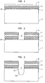
- FIGS. 1-6 show cross-sections of a silicon chip at various stages in the process of forming silicon-oxide filled trenches therein in accordance with the invention.
- the invention relates to semiconductor device fabrication.
- the invention relates to forming shallow trench isolations for separating components within the device.
- devices are processed in parallel in or on a semiconductor wafer that subsequently would be diced into individual chips comprising a device. For purposes of simplification, the processing will be described in terms of a single chip.
- the device is formed in and/or on a semiconductor wafer.
- the wafer for example, comprises monocrystalline silicon.
- a thin layer of a sacrificial oxide 11 is typically formed over an active (top) surface 13A of a chip or substrate 13 comprising, for example, silicon.
- This oxide serves primarily to protect the silicon surface during the processing.
- a layer of silicon nitride 15 (PAD nitride) that serves as an etch stop in the processing.
- PAD nitride silicon nitride 15
- Polycrystalline silicon is especially well suited for this purpose. Other materials which prevent penetration of oxygen ions, such amorphous silicon or germanium, are also useful.
- the thickness of the layer 17 advantageously should be such that it can effectively be oxidized completely in the heating that is used to anneal the implanted oxygen later in the processing.
- a mask layer 19 comprising of, for example, resist is formed and patterned, defining a trench to be etched.
- the polycrystalline layer 17, the silicon nitride 15, and the PAD silicon oxide 11 are etched away selectively in the region where the trench is to be formed, thee exposing the bare silicon surface 13A.
- etching would be done by reactive ion etching (RIE) that is capable of etching anisotropically.
- RIE reactive ion etching
- the substrate 13 is etched anisotropically in known fashion to form therein a trench 21 having an upper portion 21A with essentially vertical sidewalls.
- the height of this portion 21A is advantageously about the same as the width of the trench, which typically might be of the order of the minimum feature size, currently about 0.175 micron. However, in some instances a shallower depth, e.g., one half the width of the trench, could be adequate. Any of the known reactive ion etching (RIE) techniques known for etching trenches with essentially vertical side walls can be used for this purpose.
- RIE reactive ion etching
- portion 21B of the trench 21.
- the combined depth of portions 21A and 21B is sufficient to serve as a shallow trench isolation.
- the height of portion 21B advantageously is between about one quarter and three quarters of the width of the trench 21. Any of the RIE techniques known for etching trenches with tapered side walls can be used for this step.
- the nitride serves as a screen layer for the subsequent oxygen ion implant.
- Other material that serves as a screen implant layer which is selective to oxide is also useful.
- a combination of oxide and nitride layers is also useful.
- the oxygen implantation is done advantageously, for example, as described in a paper entitled" SIMOX-a new challenge for ion implantation" by A. Auberton et al., published in Nuclear Instruments and Methods in Physics Research B96 (1995) pp 420-424, which is herein incorporated by reference for all purposes.
- dosages of between about 4x10¹⁸ 0+/cm2 and 1x10¹⁸ 0+/cm2 with energies of about 120 KeV are described as satisfactory.
- the extent of penetration of the oxygen into the walls of the trench is indicated by the broken line 27.
- the oxygen will also be implanted in the polycrystalline layer 17 that served as a mask and this will also be converted to silicon oxide. The oxygen so implanted is not shown to keep the drawings simple.
- the substrate 13 is heated.
- the temperature at which the substrate is heated is sufficient to effectively anneal out the damage caused by the implant and also to react the implanted oxygen with the silicon to form silicon dioxide along the tapered side wall and bottom portion 21B of the trench 21 and to convert layer 17 to silicon dioxide (still shown as layer 17).
- the substrate is heated to a temperature from about 1150 - 1300°C.
- the anneal is sufficiently long to ensure the desired formation of silicon oxide where the oxygen was implanted. Typically, the anneal lasts for several hours.
- swelling occurs where the silicon and oxygen combine to form silicon oxide. This swelling tends to round off by filling sharp corners at the bottom of the trench 21 and make it easier for the silicon oxide that is subsequently to be deposited to fill the trench 21.
- the implanted silicon region at the bottom of the trench 21 is converted to oxide, its addition effectively deepens the isolation role of the trench 21.
- the silicon oxide layer created at the bottom of the trench 21 by the heating step includes both a portion of the silicon chip 13 that was converted to oxide and a portion of the original trench 21 that was filled by the swelling.
- a dielectric layer 30 deposited over the top surface of the chip comprises silicon oxide.
- This layer 30 is deposited after first removing the silicon nitride layer 25 to permit this deposited layer to merge with layer 28.
- the bottom and the sidewalls of the trench may be oxidized as necessary.
- the thickness of this layer 30 is chosen to be enough to insure that its deposition results in filling the trench 21 so that layer 30 merges with silicon dioxide region 28.
- deposition of the dielectric layer includes TEOS or HDP.
- the silicon oxide layer 30 is subjected to chemical mechanical polishing to planarize its top surface about to the level of the original PAD silicon nitride layer 15, which can serve as an etch stop, as is seen in FIG. 6.
- a portion 32 of the layer 30 remains to fill the trench 21. Any of known techniques can be used for this step.
- a chip 13 After removal of the silicon oxide layer 30, there results a chip 13, as is shown in FIG. 6, whose top (active) surface includes a silicon oxide filled trench 32 that divides the upper portion of the chip into a plurality of electrically isolated regions 33 and 34, each of which can then be used to house one or more components of the desired integrated circuit. These components would be subsequently connected together, as desired, by one or more layers of conductive patterns (not shown) over the top surface of the chip 13 in known fashion. In some instances, it may prove desirable to provide connections to some of the components to a voltage source terminal, such as ground, by way of the back surface.
- a voltage source terminal such as ground
Landscapes
- Engineering & Computer Science (AREA)
- Physics & Mathematics (AREA)
- Condensed Matter Physics & Semiconductors (AREA)
- General Physics & Mathematics (AREA)
- Manufacturing & Machinery (AREA)
- Computer Hardware Design (AREA)
- Microelectronics & Electronic Packaging (AREA)
- Power Engineering (AREA)
- Element Separation (AREA)
- Formation Of Insulating Films (AREA)
Applications Claiming Priority (2)
| Application Number | Priority Date | Filing Date | Title |
|---|---|---|---|
| US08/883,356 US5783476A (en) | 1997-06-26 | 1997-06-26 | Integrated circuit devices including shallow trench isolation |
| US883356 | 1997-06-26 |
Publications (1)
| Publication Number | Publication Date |
|---|---|
| EP0887855A1 true EP0887855A1 (en) | 1998-12-30 |
Family
ID=25382434
Family Applications (1)
| Application Number | Title | Priority Date | Filing Date |
|---|---|---|---|
| EP98109837A Ceased EP0887855A1 (en) | 1997-06-26 | 1998-05-29 | Integrated circuit devices including shallow trench isolation |
Country Status (6)
| Country | Link |
|---|---|
| US (1) | US5783476A (enExample) |
| EP (1) | EP0887855A1 (enExample) |
| JP (1) | JPH1174344A (enExample) |
| KR (1) | KR100540850B1 (enExample) |
| CN (1) | CN1133208C (enExample) |
| TW (1) | TW393722B (enExample) |
Families Citing this family (44)
| Publication number | Priority date | Publication date | Assignee | Title |
|---|---|---|---|---|
| KR100226488B1 (ko) * | 1996-12-26 | 1999-10-15 | 김영환 | 반도체 소자 격리구조 및 그 형성방법 |
| US6133123A (en) | 1997-08-21 | 2000-10-17 | Micron Technology, Inc. | Fabrication of semiconductor gettering structures by ion implantation |
| KR100275730B1 (ko) * | 1998-05-11 | 2000-12-15 | 윤종용 | 트렌치 소자분리 방법 |
| US6093619A (en) * | 1998-06-18 | 2000-07-25 | Taiwan Semiconductor Manufaturing Company | Method to form trench-free buried contact in process with STI technology |
| US6355540B2 (en) * | 1998-07-27 | 2002-03-12 | Acer Semicondutor Manufacturing Inc. | Stress-free shallow trench isolation |
| US6054364A (en) * | 1998-09-08 | 2000-04-25 | Advanced Micro Devices | Chemical mechanical polishing etch stop for trench isolation |
| US6071794A (en) * | 1999-06-01 | 2000-06-06 | Mosel Vitelic, Inc. | Method to prevent the formation of a thinner portion of insulating layer at the junction between the side walls and the bottom insulator |
| US6309937B1 (en) * | 1999-05-03 | 2001-10-30 | Vlsi Technology, Inc. | Method of making shallow junction semiconductor devices |
| TW415017B (en) * | 1999-08-11 | 2000-12-11 | Mosel Vitelic Inc | Method of improving trench isolation |
| US6350659B1 (en) | 1999-09-01 | 2002-02-26 | Agere Systems Guardian Corp. | Process of making semiconductor device having regions of insulating material formed in a semiconductor substrate |
| US6187650B1 (en) * | 1999-11-05 | 2001-02-13 | Promos Tech., Inc. | Method for improving global planarization uniformity of a silicon nitride layer used in the formation of trenches by using a sandwich stop layer |
| US6348395B1 (en) * | 2000-06-07 | 2002-02-19 | International Business Machines Corporation | Diamond as a polish-stop layer for chemical-mechanical planarization in a damascene process flow |
| US6680239B1 (en) * | 2000-07-24 | 2004-01-20 | Chartered Semiconductor Manufacturing Ltd. | Effective isolation with high aspect ratio shallow trench isolation and oxygen or field implant |
| US6432798B1 (en) * | 2000-08-10 | 2002-08-13 | Intel Corporation | Extension of shallow trench isolation by ion implantation |
| US6437417B1 (en) * | 2000-08-16 | 2002-08-20 | Micron Technology, Inc. | Method for making shallow trenches for isolation |
| TW521377B (en) * | 2000-08-29 | 2003-02-21 | Agere Syst Guardian Corp | Trench structure and method of corner rounding |
| US6524929B1 (en) | 2001-02-26 | 2003-02-25 | Advanced Micro Devices, Inc. | Method for shallow trench isolation using passivation material for trench bottom liner |
| US6486038B1 (en) | 2001-03-12 | 2002-11-26 | Advanced Micro Devices | Method for and device having STI using partial etch trench bottom liner |
| US6521510B1 (en) | 2001-03-23 | 2003-02-18 | Advanced Micro Devices, Inc. | Method for shallow trench isolation with removal of strained island edges |
| US6583488B1 (en) | 2001-03-26 | 2003-06-24 | Advanced Micro Devices, Inc. | Low density, tensile stress reducing material for STI trench fill |
| US6534379B1 (en) | 2001-03-26 | 2003-03-18 | Advanced Micro Devices, Inc. | Linerless shallow trench isolation method |
| KR20030056217A (ko) * | 2001-12-27 | 2003-07-04 | 동부전자 주식회사 | 반도체 섭스트레이트의 소자 분리 방법 |
| US6576558B1 (en) * | 2002-10-02 | 2003-06-10 | Taiwan Semiconductor Manufacturing Company | High aspect ratio shallow trench using silicon implanted oxide |
| JP2004280493A (ja) * | 2003-03-17 | 2004-10-07 | Sanyo Electric Co Ltd | 半導体素子のレイアウト設計装置、レイアウト設計方法及びレイアウト設計プログラム |
| JP2005142319A (ja) * | 2003-11-06 | 2005-06-02 | Renesas Technology Corp | 半導体装置の製造方法 |
| KR100571410B1 (ko) * | 2003-12-31 | 2006-04-14 | 동부아남반도체 주식회사 | 반도체 소자의 트랜치 소자 분리막 형성 방법 |
| US20060063338A1 (en) * | 2004-09-20 | 2006-03-23 | Lsi Logic Corporation | Shallow trench isolation depth extension using oxygen implantation |
| CN100416793C (zh) * | 2005-11-24 | 2008-09-03 | 上海华虹Nec电子有限公司 | 应用于浅沟槽隔离工艺中改善器件隔离效果的方法 |
| KR100822469B1 (ko) | 2005-12-07 | 2008-04-16 | 삼성전자주식회사 | 복수개의 소자를 상호 격리시키기 위한 에어캐비티를구비한 시스템 온 칩 구조물, 듀플렉서, 및 그 제조 방법 |
| US20070158779A1 (en) * | 2006-01-12 | 2007-07-12 | International Business Machines Corporation | Methods and semiconductor structures for latch-up suppression using a buried damage layer |
| US7648869B2 (en) * | 2006-01-12 | 2010-01-19 | International Business Machines Corporation | Method of fabricating semiconductor structures for latch-up suppression |
| US7491618B2 (en) * | 2006-01-26 | 2009-02-17 | International Business Machines Corporation | Methods and semiconductor structures for latch-up suppression using a conductive region |
| US7276768B2 (en) * | 2006-01-26 | 2007-10-02 | International Business Machines Corporation | Semiconductor structures for latch-up suppression and methods of forming such semiconductor structures |
| US20070194403A1 (en) * | 2006-02-23 | 2007-08-23 | International Business Machines Corporation | Methods for fabricating semiconductor device structures with reduced susceptibility to latch-up and semiconductor device structures formed by the methods |
| US8112817B2 (en) * | 2006-10-30 | 2012-02-07 | Girish Chiruvolu | User-centric authentication system and method |
| KR100845102B1 (ko) * | 2006-12-20 | 2008-07-09 | 동부일렉트로닉스 주식회사 | 반도체 소자의 소자분리막 형성방법 |
| US7818702B2 (en) * | 2007-02-28 | 2010-10-19 | International Business Machines Corporation | Structure incorporating latch-up resistant semiconductor device structures on hybrid substrates |
| US7754513B2 (en) * | 2007-02-28 | 2010-07-13 | International Business Machines Corporation | Latch-up resistant semiconductor structures on hybrid substrates and methods for forming such semiconductor structures |
| US8299633B2 (en) * | 2009-12-21 | 2012-10-30 | Advanced Micro Devices, Inc. | Semiconductor chip device with solder diffusion protection |
| US8956948B2 (en) * | 2010-05-20 | 2015-02-17 | Globalfoundries Inc. | Shallow trench isolation extension |
| US8399957B2 (en) | 2011-04-08 | 2013-03-19 | International Business Machines Corporation | Dual-depth self-aligned isolation structure for a back gate electrode |
| US20130043513A1 (en) | 2011-08-19 | 2013-02-21 | United Microelectronics Corporation | Shallow trench isolation structure and fabricating method thereof |
| JP6238234B2 (ja) * | 2014-06-03 | 2017-11-29 | ルネサスエレクトロニクス株式会社 | 半導体装置 |
| US10522549B2 (en) * | 2018-02-17 | 2019-12-31 | Varian Semiconductor Equipment Associates, Inc. | Uniform gate dielectric for DRAM device |
Citations (3)
| Publication number | Priority date | Publication date | Assignee | Title |
|---|---|---|---|---|
| US5183775A (en) * | 1990-01-23 | 1993-02-02 | Applied Materials, Inc. | Method for forming capacitor in trench of semiconductor wafer by implantation of trench surfaces with oxygen |
| US5393693A (en) * | 1994-06-06 | 1995-02-28 | United Microelectronics Corporation | "Bird-beak-less" field isolation method |
| EP0685882A1 (en) * | 1994-05-31 | 1995-12-06 | STMicroelectronics Limited | Semiconductor device incorporating an isolation trench and manufacture thereof |
Family Cites Families (7)
| Publication number | Priority date | Publication date | Assignee | Title |
|---|---|---|---|---|
| US4842675A (en) * | 1986-07-07 | 1989-06-27 | Texas Instruments Incorporated | Integrated circuit isolation process |
| JPH01281747A (ja) * | 1988-05-09 | 1989-11-13 | Nec Corp | 絶縁膜埋込みトレンチの形成方法 |
| JPH01295438A (ja) * | 1988-05-24 | 1989-11-29 | Matsushita Electric Ind Co Ltd | 半導体装置の製造方法 |
| JPH0437152A (ja) * | 1990-06-01 | 1992-02-07 | Fujitsu Ltd | 半導体装置の製造方法 |
| US5565376A (en) * | 1994-07-12 | 1996-10-15 | United Microelectronics Corp. | Device isolation technology by liquid phase deposition |
| US5445989A (en) * | 1994-08-23 | 1995-08-29 | United Microelectronics Corp. | Method of forming device isolation regions |
| KR0186083B1 (ko) * | 1995-08-12 | 1999-04-15 | 문정환 | 반도체 소자의 소자격리방법 |
-
1997
- 1997-06-26 US US08/883,356 patent/US5783476A/en not_active Expired - Lifetime
-
1998
- 1998-05-29 EP EP98109837A patent/EP0887855A1/en not_active Ceased
- 1998-06-15 TW TW087109460A patent/TW393722B/zh not_active IP Right Cessation
- 1998-06-17 CN CN98114904A patent/CN1133208C/zh not_active Expired - Fee Related
- 1998-06-19 KR KR1019980023051A patent/KR100540850B1/ko not_active Expired - Fee Related
- 1998-06-25 JP JP10178739A patent/JPH1174344A/ja not_active Withdrawn
Patent Citations (3)
| Publication number | Priority date | Publication date | Assignee | Title |
|---|---|---|---|---|
| US5183775A (en) * | 1990-01-23 | 1993-02-02 | Applied Materials, Inc. | Method for forming capacitor in trench of semiconductor wafer by implantation of trench surfaces with oxygen |
| EP0685882A1 (en) * | 1994-05-31 | 1995-12-06 | STMicroelectronics Limited | Semiconductor device incorporating an isolation trench and manufacture thereof |
| US5393693A (en) * | 1994-06-06 | 1995-02-28 | United Microelectronics Corporation | "Bird-beak-less" field isolation method |
Also Published As
| Publication number | Publication date |
|---|---|
| US5783476A (en) | 1998-07-21 |
| KR100540850B1 (ko) | 2006-02-28 |
| TW393722B (en) | 2000-06-11 |
| CN1133208C (zh) | 2003-12-31 |
| CN1204148A (zh) | 1999-01-06 |
| JPH1174344A (ja) | 1999-03-16 |
| KR19990007123A (ko) | 1999-01-25 |
Similar Documents
| Publication | Publication Date | Title |
|---|---|---|
| US5783476A (en) | Integrated circuit devices including shallow trench isolation | |
| US5811347A (en) | Nitrogenated trench liner for improved shallow trench isolation | |
| KR100226488B1 (ko) | 반도체 소자 격리구조 및 그 형성방법 | |
| US5679599A (en) | Isolation using self-aligned trench formation and conventional LOCOS | |
| US5229316A (en) | Semiconductor processing method for forming substrate isolation trenches | |
| US6437417B1 (en) | Method for making shallow trenches for isolation | |
| US5904541A (en) | Method for fabricating a semiconductor device having a shallow trench isolation structure | |
| US6143624A (en) | Shallow trench isolation formation with spacer-assisted ion implantation | |
| JP2002324905A (ja) | ボディ・コンタクトを有する集積回路の形成方法 | |
| US6784042B2 (en) | Integration process on a SOI substrate of a semiconductor device comprising at least a dielectrically isolated well | |
| US5733813A (en) | Method for forming planarized field isolation regions | |
| EP0540262A2 (en) | Trench isolation region | |
| US5950097A (en) | Advanced isolation scheme for deep submicron technology | |
| US6680239B1 (en) | Effective isolation with high aspect ratio shallow trench isolation and oxygen or field implant | |
| CN113113423A (zh) | Soi上的深沟槽隔离和衬底连接 | |
| US6344374B1 (en) | Method of fabricating insulators for isolating electronic devices | |
| US20010001723A1 (en) | Nitrogenated trench liner for improved shallow trench isolation | |
| US6281093B1 (en) | Method to reduce trench cone formation in the fabrication of shallow trench isolations | |
| HK1015533A (en) | Integrated circuit devices including shallow trench isolation | |
| KR100355870B1 (ko) | 반도체 소자 분리를 위한 얕은 트렌치 제조 방법 | |
| KR100200751B1 (ko) | 반도체장치의 소자분리방법 | |
| KR100562268B1 (ko) | 반도체 소자의 소자분리막형성방법 | |
| KR100596876B1 (ko) | 반도체 소자의 소자 분리막 형성 방법 | |
| KR20010038607A (ko) | 반도체장치를 위한 필드 분리방법 | |
| US6103593A (en) | Method and system for providing a contact on a semiconductor device |
Legal Events
| Date | Code | Title | Description |
|---|---|---|---|
| PUAI | Public reference made under article 153(3) epc to a published international application that has entered the european phase |
Free format text: ORIGINAL CODE: 0009012 |
|
| AK | Designated contracting states |
Kind code of ref document: A1 Designated state(s): DE FR GB IE IT NL |
|
| AX | Request for extension of the european patent |
Free format text: AL;LT;LV;MK;RO;SI |
|
| AKX | Designation fees paid | ||
| 17P | Request for examination filed |
Effective date: 19990406 |
|
| RBV | Designated contracting states (corrected) |
Designated state(s): DE FR GB IE IT NL |
|
| RAP1 | Party data changed (applicant data changed or rights of an application transferred) |
Owner name: INFINEON TECHNOLOGIES AG |
|
| REG | Reference to a national code |
Ref country code: HK Ref legal event code: WD Ref document number: 1015533 Country of ref document: HK |
|
| STAA | Information on the status of an ep patent application or granted ep patent |
Free format text: STATUS: THE APPLICATION HAS BEEN REFUSED |
|
| 18R | Application refused |
Effective date: 20080817 |