EP0886865B1 - Cell plate referencing for dram sensing - Google Patents
Cell plate referencing for dram sensing Download PDFInfo
- Publication number
- EP0886865B1 EP0886865B1 EP96918166A EP96918166A EP0886865B1 EP 0886865 B1 EP0886865 B1 EP 0886865B1 EP 96918166 A EP96918166 A EP 96918166A EP 96918166 A EP96918166 A EP 96918166A EP 0886865 B1 EP0886865 B1 EP 0886865B1
- Authority
- EP
- European Patent Office
- Prior art keywords
- digit line
- transistor
- node
- sense amplifier
- sensing
- Prior art date
- Legal status (The legal status is an assumption and is not a legal conclusion. Google has not performed a legal analysis and makes no representation as to the accuracy of the status listed.)
- Expired - Lifetime
Links
Images
Classifications
-
- G—PHYSICS
- G11—INFORMATION STORAGE
- G11C—STATIC STORES
- G11C11/00—Digital stores characterised by the use of particular electric or magnetic storage elements; Storage elements therefor
- G11C11/21—Digital stores characterised by the use of particular electric or magnetic storage elements; Storage elements therefor using electric elements
- G11C11/34—Digital stores characterised by the use of particular electric or magnetic storage elements; Storage elements therefor using electric elements using semiconductor devices
- G11C11/40—Digital stores characterised by the use of particular electric or magnetic storage elements; Storage elements therefor using electric elements using semiconductor devices using transistors
- G11C11/401—Digital stores characterised by the use of particular electric or magnetic storage elements; Storage elements therefor using electric elements using semiconductor devices using transistors forming cells needing refreshing or charge regeneration, i.e. dynamic cells
- G11C11/4063—Auxiliary circuits, e.g. for addressing, decoding, driving, writing, sensing or timing
- G11C11/407—Auxiliary circuits, e.g. for addressing, decoding, driving, writing, sensing or timing for memory cells of the field-effect type
- G11C11/4074—Power supply or voltage generation circuits, e.g. bias voltage generators, substrate voltage generators, back-up power, power control circuits
-
- G—PHYSICS
- G11—INFORMATION STORAGE
- G11C—STATIC STORES
- G11C11/00—Digital stores characterised by the use of particular electric or magnetic storage elements; Storage elements therefor
- G11C11/21—Digital stores characterised by the use of particular electric or magnetic storage elements; Storage elements therefor using electric elements
- G11C11/34—Digital stores characterised by the use of particular electric or magnetic storage elements; Storage elements therefor using electric elements using semiconductor devices
- G11C11/40—Digital stores characterised by the use of particular electric or magnetic storage elements; Storage elements therefor using electric elements using semiconductor devices using transistors
- G11C11/401—Digital stores characterised by the use of particular electric or magnetic storage elements; Storage elements therefor using electric elements using semiconductor devices using transistors forming cells needing refreshing or charge regeneration, i.e. dynamic cells
- G11C11/4063—Auxiliary circuits, e.g. for addressing, decoding, driving, writing, sensing or timing
- G11C11/407—Auxiliary circuits, e.g. for addressing, decoding, driving, writing, sensing or timing for memory cells of the field-effect type
- G11C11/409—Read-write [R-W] circuits
- G11C11/4094—Bit-line management or control circuits
Definitions
- the present invention relates generally to dynamic memory integrated circuits and in particular the present invention relates to sensing circuits therein.
- Integrated circuit memories have become increasingly dense as the need for more memory storage increases. While fabrication techniques and design options have been fairly successful in maintaining steady increases in memory storage from design generation to generation, the need for new highly populated circuits continues.
- a dynamic random access memory (DRAM) device is comprised of an arrangement of individual memory cells.
- Each memory cell comprises a capacitor capable of holding a charge and an access transistor for accessing the capacitor charge.
- the charge is referred to as a data bit and can be either a high voltage or a low voltage.
- Data can be either stored in the memory cells during a write mode, or data may be retrieved from the memory cells during a read mode.
- the data is transmitted on signal lines, referred to as digit lines, which are coupled to input/output lines through transistors used as switching devices. For each bit of data stored, its true logic state is available on an I/O line and its complementary logic state is available at on an I/O complement line. Thus, each memory cell has two digit lines, digit and digit complement.
- the memory cells are arranged in an array and each cell has an address identifying its location in the array.
- the array comprises a configuration of intersecting rows and a memory cell is associated with each intersection.
- the address for the selected cell is represented by input signals to a row decoder and to a column decoder.
- the row decoder activates a word line in response to the row address.
- the selected word line activates the access transistors for each of the memory cells in communication with the selected word line.
- the column decoder selects a digit line pair in response to the column address. For a read operation the selected word line activates the access transistors for a given row address, and data is latched to the digit line pairs.
- Conventional dynamic memories use memory cells fabricated as capacitors in an integrated circuit to store data. That is, a logical "I" is stored as a charge on the capacitor and the capacitor is discharged for a logical "O".
- the pairs of digit lines are fabricated as metal lines on the integrated circuit and connected to the memory cells for transmitting data stored in the memory cells.
- Sense amplifiers are utilized to sense small differentials on the digit lines and drive the digit lines to full power supply rails for either reading the memory cells or writing thereto.
- a dynamic memory circuit is described in a preferred embodiment which uses sensing circuitry that reduces the number of metal digit lines needed to access the memory cells by using the common cell plate as a reference for sensing circuitry.
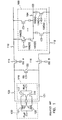
- a memory array 100 has a plurality of memory cells 102(0)-(n) which are fabricated as capacitors having one capacitive plate formed as a common cell plate 104 and the other node connected to an access transistor 106(0)-(n).
- Each access transistor is a n-type transistor having its gate connected to a word line 108(0)-(n).
- the cell plate 104 is typically biased to one-half the power supply voltage (Vcc) by a biasing source (not shown).
- Digit lines 110 and 112 are each connected to some of the access transistors and memory cells. When access transistors 106 are selectively activated, the charge stored on the corresponding memory cell 102 is coupled to one of the digit lines.
- N-type isolation transistors 114 and 116 are used to isolate digit lines 110 and 112, respectively, from both the n-sense amp 118 and the p-sense amp 120.
- Equilibrate transistor 122 is used to equalize the nodes of the sense amps to the same voltage, as described below.
- the first step is to equilibrate nodes 129 and 131 of sense amps 118 and 120 to Vcc/2, as sourced by a biasing circuit (not shown), by holding the gate of transistor 122 (EQ) high.
- the differential voltage across the sense amps is therefore zero with each node having a preferred voltage of one-half the supply voltage (Vcc).
- the next step is to activate isolation transistors 114 and 116 by providing their gates (ISO A and ISO B, respectively) with a high voltage. This connects the digit lines 110 and 112 to the sense amps 118 and 120 and allows the digit lines to also stabilize to Vcc/2.
- One of the memory cell access transistors 106(0)-(n) is then selectively activated by raising the associated word line 108(0)-(n) gate voltage.
- the charge, or lack of charge, stored on the selected memory cell 102 is then shared with one of the digit lines. If a logical "one" is stored on the capacitor the associated digit line will be slightly raised, for example by a voltage of approximately 100 mv. It will be understood that the charge shared with the digit line is directly dependent upon the charge stored on the memory cell. If the memory cell is un-charged the digit line voltage will drop, for example by 100 mv.
- n-sense amp 118 and the p-sense amp 120 sense a differential between the digit lines and drive the digit lines to full rails in response.
- N-sense amp 118 has two n-channel transistors having their gates cross-coupled to the source of the other transistor. The drains of each transistor are connected together and controlled by an NLat line.
- the NLat line is typically pre-charged to the same level that nodes 129 and 131 have been equalized to, Vcc/2. The voltage on the NLat line is lowered to sense a high voltage on one of the nodes.
- transistor 119 will begin to turn on when the NLat drops by a threshold voltage below node 129. Node 131 will then be pulled to NLat to insure that transistor 117 does not turn on.
- p-sense amp 120 has two cross-coupled p-channel transistors 121 and 125. The drains of each transistor are connected together and controlled by a PLat line.
- the PLat line is typically pre-charged to the same level that the nodes 129 and 131 have been equalized to, Vcc/2. The voltage on the PLat line is raised to sense a low voltage on one of the nodes.
- transistor 121 will begin to turn on when the PLat increases by a threshold voltage above node 131. Node 129 will then be pulled to PLat to insure that transistor 125 does not turn on.
- the NLat and PLat are strobed to full power rails, ground and Vcc, respectively. If one of the digit lines is higher, therefore, that digit line will be driven to Vcc while the complementary digit line is pulled to ground.
- the voltage on the digit lines are equal until shortly after the word line is activated.
- the n-sense amp is strobed first to drive one line low and then the p-sense amp is strobed to drive the other line high.
- the digit lines remain latched at these full power levels until the equilibrate transistor 122 is again activated. During the time in which the word line is high and the digit lines are latched, the memory cell is refreshed.
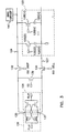
- a memory array 123 is comprised of memory cells 126(0)-(n) fabricated as capacitors with one node connected to a common cell plate 127.
- the cell plate is biased to one-half Vcc by a biasing circuit (not shown).
- the other plate of each memory cell 126 is connected to one of the n-type access transistors 128(0)-(n).
- the access transistors are connected to digit line 124 and have their gate connected one of the word lines 130(0)-(n).
- Isolation transistors 132 and 134 are provided to. selectively isolate digit line 124 and cell plate 127, respectively, from the n-sense amp 136 and the p-sense amp 138 nodes 135 and 137.
- N-type equilibrate transistor 139 is provided to equalize the sense amp nodes 135 and 137 to a common voltage.
- the digit line 124 and the cell plate are equalized by activating the gate of transistor 139 (EQ).
- the cell plate is held to Vcc/2, as such the digit line is also held to Vcc/2.
- the equilibrate transistor I -'19 is turned off.
- Isolation transistor 134 is then turned off by lowering its gate voltage (ISO Cell) to isolate node 137 of the sense amps from the cell plate 127.
- the voltage at node 137 is coupled down when transistor 139 is turned off. For example, the voltage on node 137 drops by approximately 20 mv when transistor 139 is turned off.
- isolation transistor 132 is turned off by lowering its gate voltage (ISO Digit) to isolate node 135 from the digit line.
- ISO Digit gate voltage
- the sense amps are then strobed using NLat and PLat to drive node 135 to the appropriate supply level, as known to one skilled in the art. That is, if node 135 is above the equilibrate level, the node is driven to Vcc and if node 135 is below the equilibrate level it is driven to ground. Isolation transistor 132 is then re-activated by raising ISO Digit so that the entire digit line 124 can go to the appropriate power rail and the memory cell can be refreshed.
- the equilibrate transistor can be re-activated to insure that both nodes of the sense amps and the digit line are at a stable equivalent voltage near Vcc/2 prior to activating isolation transistor 134 (ISO Cell). Connecting nodes 135 and 137 through transistor 139 while the sense amps are activated will result in a crossing current in the sense amps. This crossing current can be relatively large and economically undesirable. It will be understood that when one sense arnp node is originally at Vcc and the other is at ground, the resulting equilibrate level will be near Vcc/2. The bias level of cell plate 127, therefore, remains substantially unaffected.
- the circuit maintains the memory cell differential voltage over a wide change in supply voltage without substantial lose in cell margin.
- the related art loses cell margin in the supply voltage changes after data has been written to a memory cell because the reference voltage was independently based on the supply voltage.
- the reference voltage and the memory cell both depend upon the cell plate, so that changes in the reference voltage are reflected on the digit line and cell margin is not effected.
- Isolation transistor 133 can be used to selectively connect node 137 to the digit line 124 to equilibrate the sense amps by forcing node 137 to its opposite state. That is, by first isolating node 135 from the digit line 124 and then activating transistor 133, the sense amps will force the voltage on the digit line to change its state. If, for example, the digit line is a "one" when transistor 133 is activated, the voltage on the digit line will be forced to transition low by the n-sense amp. It will be understood that by holding node 135 constant and using transistor 133, crossing currents are avoided.
- a trigger or tracking circuit (not shown) can be used to latch the voltage at a level near Vcc/2. One embodiment would be to use a timing circuit to turn on equilibrate transistor 139 and turn off the sense amps 136 and 138.
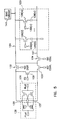
- FIG. 6 illustrates the timing of this equilibrate circuit.
- Equilibrate transistor 139 is turned off by lowering its gate voltage (EQ).
- the isolation transistor 134 is turned off by lowering its gate (ISO Cell) to isolate the cell plate from the circuit.
- a word line 130 is raised to access a memory cell 126 and transistor 132 is de-activated by lowering its gate voltage (ISO Digit).
- the sense amps are strobed using NLat and PLat and transistor 132 is re-activated to refresh the memory cell.
- transistor 132 is turned off to isolate digit line 124 from node 135.
- Transistor 133 is activated by raising its gate voltage (ISO Equil) and node 137 is connected to the digit line.
- the sense amps will force the digit line to begin to change states by either charging or discharging the digit line.
- a timing or trigger circuit will activate equilibrate transistor 139 and turn off the sense amps. Both nodes 135 and 137 are therefore equalized and transistors 132 and 134 are activated. Finally, transistor 133 is turned off and the bias level of cell plate 127 remains substantially unaffected.
- An optional bias circuit 141 is shown in Figure 3. This circuit can be used to bias the digit line 142 to a voltage level of Vcc/2. By activating transistors 132 and 139 the nodes of the sense amps could be equilibrated to Vcc/2 prior to activating transistor 134. This equilibrate option requires additional die area and is therefore economically less desirable then the other equilibrate circuits.
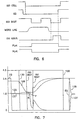
- FIG 7 is a more detailed diagram of a sensing operation on a selected memory cell which contains data stored as a "one" in the circuit of Figure 3. It can be seen that prior to the gate of transistor 139 (EQ) falling from Vcc (3.6 volts) the sense amp nodes 135 and 137 are equalized at 1.8 volts (Vcc/2). Node 137 is coupled low when EQ goes low, thereby, creating a small differential between nodes 135 and 137. One of the memory cells 126 is selected by raising its associated word line 130. The charge stored on the memory cell is shared with the digit line 124 and node 135.
- the capacitance of the digit line is higher than the capacitance of the memory cell, thus the voltage of node 135 only increases by a fraction,of the drop in voltage on the memory cell.
- Transistor 132 is turned off by lowering the ISO Digit line. As a result, node 135 is coupled low and the differential voltage between the sense amp nodes reflects a true value of the memory cell charge.
- the n-sense amp 136 is strobed (shown as point N) and then the p-sense amp 138 is strobed (shown as point P).
- node 135 is coupled low after the n-sense amp is strobed, but is pulled high when the p-sense amp is strobed.
- Transistor 132 is re-activated to connect node 135 to the digit line and memory cell 126. Both nodes of the sense amps are coupled high when the ISO Digit line goes high. Node 135 is pulled high by the p-sense amp and node 137 is pulled low by the n-sense amp.
- the memory cell is refreshed during the time that both transistor 132 and transistor 130 are activated. That is, the voltage on memory cell 126 is pulled to Vcc to re-charge the cell.
- transistors 132 and 130 are connected to a pump voltage which has a high level above Vcc, as known to one skilled in the art.
- the EQ line returns high to activate transistor 139 and nodes 135 and 137 are equilibrated to Vcc/2 prior to connecting node 137 to the cell plate.
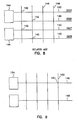
- the related integrated circuit uses two digit lines 140 to connect memory cells 142 to each sense amp 144.
- the memory cells are arranged such that the intersection of every-other row line 146 and every-other digit line have a memory cell 142.
- Each sense amp 144 can, therefore, selectively sense four different memory cells in this illustration. It can be seen that any reductions in memory cell size cannot be fully realized do to the layout spacing requirements.
- Figure 9 illustrates an integrated circuit incorporating the cell plate biasing of the present invention.
- Memory cells 150 are located at each intersection of digit lines 148 and row lines 152.
- Sense amp circuits 154 are biased using the cell plate, as described above, and can selectively sense four different memory cells in this illustration.
- the present invention allows the use 6F 2 size memory cells where the conventional circuit used 8F 2 memory cells, where F is the device feature size as known by one skilled in the art.
- the integrated circuit uses one digit line and the memory cell plate for sensing charges stored on memory cell capacitors. Because the cell plate is a pre-existing structure in the integrated circuit, the elimination of one digit line allows the miniaturization of memory cells and associated circuits to be fully exploited. Three circuits have been described which could be used to equalize the sense amp nodes prior to sensing a memory cell charge. By using the cell plate as a reference, a full differential is maintained and no cell margin is lost due to variations in supply voltage.
Landscapes
- Engineering & Computer Science (AREA)
- Microelectronics & Electronic Packaging (AREA)
- Computer Hardware Design (AREA)
- Dram (AREA)
- Transceivers (AREA)
- Stabilization Of Oscillater, Synchronisation, Frequency Synthesizers (AREA)
- Semiconductor Memories (AREA)
- Investigating Or Analysing Biological Materials (AREA)
- Debugging And Monitoring (AREA)
Applications Claiming Priority (3)
| Application Number | Priority Date | Filing Date | Title |
|---|---|---|---|
| US471861 | 1995-06-06 | ||
| US08/471,861 US5719813A (en) | 1995-06-06 | 1995-06-06 | Cell plate referencing for DRAM sensing |
| PCT/US1996/009070 WO1996039698A1 (en) | 1995-06-06 | 1996-06-04 | Cell plate referencing for dram sensing |
Publications (2)
| Publication Number | Publication Date |
|---|---|
| EP0886865A1 EP0886865A1 (en) | 1998-12-30 |
| EP0886865B1 true EP0886865B1 (en) | 2001-10-04 |
Family
ID=23873269
Family Applications (1)
| Application Number | Title | Priority Date | Filing Date |
|---|---|---|---|
| EP96918166A Expired - Lifetime EP0886865B1 (en) | 1995-06-06 | 1996-06-04 | Cell plate referencing for dram sensing |
Country Status (9)
| Country | Link |
|---|---|
| US (2) | US5719813A (enExample) |
| EP (1) | EP0886865B1 (enExample) |
| JP (1) | JP3357898B2 (enExample) |
| KR (1) | KR100284467B1 (enExample) |
| AT (1) | ATE206556T1 (enExample) |
| AU (1) | AU6048996A (enExample) |
| DE (1) | DE69615712T2 (enExample) |
| TW (1) | TW307011B (enExample) |
| WO (1) | WO1996039698A1 (enExample) |
Families Citing this family (8)
| Publication number | Priority date | Publication date | Assignee | Title |
|---|---|---|---|---|
| US5719813A (en) * | 1995-06-06 | 1998-02-17 | Micron Technology, Inc. | Cell plate referencing for DRAM sensing |
| US5901078A (en) * | 1997-06-19 | 1999-05-04 | Micron Technology, Inc. | Variable voltage isolation gate and method |
| US6292387B1 (en) | 2000-01-20 | 2001-09-18 | Micron Technology, Inc. | Selective device coupling |
| US6301175B1 (en) | 2000-07-26 | 2001-10-09 | Micron Technology, Inc. | Memory device with single-ended sensing and low voltage pre-charge |
| US6292417B1 (en) | 2000-07-26 | 2001-09-18 | Micron Technology, Inc. | Memory device with reduced bit line pre-charge voltage |
| DE10302650B4 (de) * | 2003-01-23 | 2007-08-30 | Infineon Technologies Ag | RAM-Speicher und Steuerungsverfahren dafür |
| US7372092B2 (en) * | 2005-05-05 | 2008-05-13 | Micron Technology, Inc. | Memory cell, device, and system |
| US12347476B1 (en) * | 2022-12-27 | 2025-07-01 | Kepler Computing Inc. | Apparatus and method to improve sensing noise margin in a non-linear polar material based bit-cell |
Family Cites Families (16)
| Publication number | Priority date | Publication date | Assignee | Title |
|---|---|---|---|---|
| US4598387A (en) | 1983-09-29 | 1986-07-01 | Advanced Micro Devices, Inc. | Capacitive memory signal doubler cell |
| JPS60239993A (ja) * | 1984-05-12 | 1985-11-28 | Sharp Corp | ダイナミツク型半導体記憶装置 |
| US4715015A (en) * | 1984-06-01 | 1987-12-22 | Sharp Kabushiki Kaisha | Dynamic semiconductor memory with improved sense signal |
| JPS6177193A (ja) * | 1984-09-25 | 1986-04-19 | Toshiba Corp | ダイナミツク型メモリ |
| JPS62184691A (ja) * | 1986-02-08 | 1987-08-13 | Fujitsu Ltd | 半導体記憶装置 |
| JPH0336763A (ja) * | 1989-07-03 | 1991-02-18 | Hitachi Ltd | 半導体集積回路装置 |
| US5241503A (en) * | 1991-02-25 | 1993-08-31 | Motorola, Inc. | Dynamic random access memory with improved page-mode performance and method therefor having isolator between memory cells and sense amplifiers |
| JPH05159575A (ja) * | 1991-12-04 | 1993-06-25 | Oki Electric Ind Co Ltd | ダイナミックランダムアクセスメモリ |
| JPH05182458A (ja) * | 1991-12-26 | 1993-07-23 | Toshiba Corp | 半導体記憶装置 |
| JPH05242672A (ja) * | 1992-02-04 | 1993-09-21 | Nec Corp | 半導体ダイナミックメモリ |
| KR950009234B1 (ko) * | 1992-02-19 | 1995-08-18 | 삼성전자주식회사 | 반도체 메모리장치의 비트라인 분리클럭 발생장치 |
| JP3020345B2 (ja) * | 1992-05-19 | 2000-03-15 | 株式会社 沖マイクロデザイン | 半導体記憶回路 |
| JPH06215564A (ja) * | 1993-01-13 | 1994-08-05 | Nec Corp | 半導体記憶装置 |
| JPH0785675A (ja) * | 1993-09-17 | 1995-03-31 | Mitsubishi Electric Corp | 半導体記憶装置 |
| US5719813A (en) * | 1995-06-06 | 1998-02-17 | Micron Technology, Inc. | Cell plate referencing for DRAM sensing |
| US5648749A (en) * | 1995-09-19 | 1997-07-15 | Lin; Kuang Ts'an | Cartridge fuse mounting structure |
-
1995
- 1995-06-06 US US08/471,861 patent/US5719813A/en not_active Expired - Lifetime
-
1996
- 1996-06-04 WO PCT/US1996/009070 patent/WO1996039698A1/en not_active Ceased
- 1996-06-04 DE DE69615712T patent/DE69615712T2/de not_active Expired - Lifetime
- 1996-06-04 KR KR1019970709066A patent/KR100284467B1/ko not_active Expired - Fee Related
- 1996-06-04 EP EP96918166A patent/EP0886865B1/en not_active Expired - Lifetime
- 1996-06-04 AT AT96918166T patent/ATE206556T1/de not_active IP Right Cessation
- 1996-06-04 JP JP50147997A patent/JP3357898B2/ja not_active Expired - Fee Related
- 1996-06-04 AU AU60489/96A patent/AU6048996A/en not_active Abandoned
- 1996-06-26 TW TW085107682A patent/TW307011B/zh not_active IP Right Cessation
-
1998
- 1998-02-17 US US09/024,440 patent/US5894444A/en not_active Expired - Lifetime
Also Published As
| Publication number | Publication date |
|---|---|
| AU6048996A (en) | 1996-12-24 |
| KR100284467B1 (ko) | 2001-03-02 |
| TW307011B (enExample) | 1997-06-01 |
| DE69615712T2 (de) | 2002-04-18 |
| US5719813A (en) | 1998-02-17 |
| US5894444A (en) | 1999-04-13 |
| KR19990022585A (ko) | 1999-03-25 |
| EP0886865A1 (en) | 1998-12-30 |
| WO1996039698A1 (en) | 1996-12-12 |
| JPH10507863A (ja) | 1998-07-28 |
| ATE206556T1 (de) | 2001-10-15 |
| JP3357898B2 (ja) | 2002-12-16 |
| DE69615712D1 (de) | 2001-11-08 |
Similar Documents
| Publication | Publication Date | Title |
|---|---|---|
| US5608668A (en) | Dram wtih open digit lines and array edge reference sensing | |
| US5856939A (en) | Low voltage dynamic memory | |
| US4855628A (en) | Sense amplifier for high performance dram | |
| EP0830685B1 (en) | Single-ended sensing using global bit lines for dram | |
| KR960002819B1 (ko) | 반도체 기억 장치 | |
| US5339274A (en) | Variable bitline precharge voltage sensing technique for DRAM structures | |
| EP0129651A2 (en) | Dynamic semiconductor memory having sensing amplifiers | |
| US6438049B1 (en) | Variable equilibrate voltage circuit for paired digit lines | |
| JPH057796B2 (enExample) | ||
| US4397003A (en) | Dynamic random access memory | |
| EP1433179B1 (en) | System and method for early write to memory by holding bitline at fixed potential | |
| US6301175B1 (en) | Memory device with single-ended sensing and low voltage pre-charge | |
| US6292417B1 (en) | Memory device with reduced bit line pre-charge voltage | |
| EP0886865B1 (en) | Cell plate referencing for dram sensing | |
| US5745423A (en) | Low power precharge circuit for a dynamic random access memory | |
| US4409672A (en) | Dynamic semiconductor memory device | |
| US20010006482A1 (en) | Equilibrate method for dynamic plate sensing memories | |
| US5710738A (en) | Low power dynamic random access memory | |
| JP2980368B2 (ja) | ダイナミック型半導体記憶装置 | |
| US4926381A (en) | Semiconductor memory circuit with sensing arrangement free from malfunction | |
| US4734890A (en) | Dynamic RAM having full-sized dummy cell | |
| US6111803A (en) | Reduced cell voltage for memory device | |
| US5276645A (en) | Semiconductor memory with reduced peak current |
Legal Events
| Date | Code | Title | Description |
|---|---|---|---|
| PUAI | Public reference made under article 153(3) epc to a published international application that has entered the european phase |
Free format text: ORIGINAL CODE: 0009012 |
|
| 17P | Request for examination filed |
Effective date: 19971203 |
|
| AK | Designated contracting states |
Kind code of ref document: A1 Designated state(s): AT BE CH DE DK ES FI FR GB GR IE IT LI LU MC NL PT SE |
|
| 17Q | First examination report despatched |
Effective date: 19991109 |
|
| GRAG | Despatch of communication of intention to grant |
Free format text: ORIGINAL CODE: EPIDOS AGRA |
|
| GRAG | Despatch of communication of intention to grant |
Free format text: ORIGINAL CODE: EPIDOS AGRA |
|
| GRAG | Despatch of communication of intention to grant |
Free format text: ORIGINAL CODE: EPIDOS AGRA |
|
| GRAH | Despatch of communication of intention to grant a patent |
Free format text: ORIGINAL CODE: EPIDOS IGRA |
|
| GRAH | Despatch of communication of intention to grant a patent |
Free format text: ORIGINAL CODE: EPIDOS IGRA |
|
| GRAA | (expected) grant |
Free format text: ORIGINAL CODE: 0009210 |
|
| AK | Designated contracting states |
Kind code of ref document: B1 Designated state(s): AT BE CH DE DK ES FI FR GB GR IE IT LI LU MC NL PT SE |
|
| PG25 | Lapsed in a contracting state [announced via postgrant information from national office to epo] |
Ref country code: NL Free format text: LAPSE BECAUSE OF FAILURE TO SUBMIT A TRANSLATION OF THE DESCRIPTION OR TO PAY THE FEE WITHIN THE PRESCRIBED TIME-LIMIT Effective date: 20011004 Ref country code: LI Free format text: LAPSE BECAUSE OF FAILURE TO SUBMIT A TRANSLATION OF THE DESCRIPTION OR TO PAY THE FEE WITHIN THE PRESCRIBED TIME-LIMIT Effective date: 20011004 Ref country code: FI Free format text: LAPSE BECAUSE OF FAILURE TO SUBMIT A TRANSLATION OF THE DESCRIPTION OR TO PAY THE FEE WITHIN THE PRESCRIBED TIME-LIMIT Effective date: 20011004 Ref country code: CH Free format text: LAPSE BECAUSE OF FAILURE TO SUBMIT A TRANSLATION OF THE DESCRIPTION OR TO PAY THE FEE WITHIN THE PRESCRIBED TIME-LIMIT Effective date: 20011004 Ref country code: BE Free format text: LAPSE BECAUSE OF FAILURE TO SUBMIT A TRANSLATION OF THE DESCRIPTION OR TO PAY THE FEE WITHIN THE PRESCRIBED TIME-LIMIT Effective date: 20011004 Ref country code: AT Free format text: LAPSE BECAUSE OF FAILURE TO SUBMIT A TRANSLATION OF THE DESCRIPTION OR TO PAY THE FEE WITHIN THE PRESCRIBED TIME-LIMIT Effective date: 20011004 |
|
| REF | Corresponds to: |
Ref document number: 206556 Country of ref document: AT Date of ref document: 20011015 Kind code of ref document: T |
|
| REG | Reference to a national code |
Ref country code: CH Ref legal event code: EP |
|
| REF | Corresponds to: |
Ref document number: 69615712 Country of ref document: DE Date of ref document: 20011108 |
|
| REG | Reference to a national code |
Ref country code: IE Ref legal event code: FG4D |
|
| REG | Reference to a national code |
Ref country code: GB Ref legal event code: IF02 |
|
| PG25 | Lapsed in a contracting state [announced via postgrant information from national office to epo] |
Ref country code: SE Free format text: LAPSE BECAUSE OF FAILURE TO SUBMIT A TRANSLATION OF THE DESCRIPTION OR TO PAY THE FEE WITHIN THE PRESCRIBED TIME-LIMIT Effective date: 20020104 Ref country code: PT Free format text: LAPSE BECAUSE OF FAILURE TO SUBMIT A TRANSLATION OF THE DESCRIPTION OR TO PAY THE FEE WITHIN THE PRESCRIBED TIME-LIMIT Effective date: 20020104 Ref country code: DK Free format text: LAPSE BECAUSE OF FAILURE TO SUBMIT A TRANSLATION OF THE DESCRIPTION OR TO PAY THE FEE WITHIN THE PRESCRIBED TIME-LIMIT Effective date: 20020104 |
|
| PG25 | Lapsed in a contracting state [announced via postgrant information from national office to epo] |
Ref country code: GR Free format text: LAPSE BECAUSE OF FAILURE TO SUBMIT A TRANSLATION OF THE DESCRIPTION OR TO PAY THE FEE WITHIN THE PRESCRIBED TIME-LIMIT Effective date: 20020105 |
|
| ET | Fr: translation filed | ||
| NLV1 | Nl: lapsed or annulled due to failure to fulfill the requirements of art. 29p and 29m of the patents act | ||
| REG | Reference to a national code |
Ref country code: CH Ref legal event code: PL |
|
| PG25 | Lapsed in a contracting state [announced via postgrant information from national office to epo] |
Ref country code: ES Free format text: LAPSE BECAUSE OF FAILURE TO SUBMIT A TRANSLATION OF THE DESCRIPTION OR TO PAY THE FEE WITHIN THE PRESCRIBED TIME-LIMIT Effective date: 20020430 |
|
| PG25 | Lapsed in a contracting state [announced via postgrant information from national office to epo] |
Ref country code: MC Free format text: LAPSE BECAUSE OF NON-PAYMENT OF DUE FEES Effective date: 20020604 Ref country code: LU Free format text: LAPSE BECAUSE OF NON-PAYMENT OF DUE FEES Effective date: 20020604 Ref country code: IE Free format text: LAPSE BECAUSE OF NON-PAYMENT OF DUE FEES Effective date: 20020604 |
|
| PLBE | No opposition filed within time limit |
Free format text: ORIGINAL CODE: 0009261 |
|
| STAA | Information on the status of an ep patent application or granted ep patent |
Free format text: STATUS: NO OPPOSITION FILED WITHIN TIME LIMIT |
|
| 26N | No opposition filed | ||
| REG | Reference to a national code |
Ref country code: IE Ref legal event code: MM4A |
|
| PGFP | Annual fee paid to national office [announced via postgrant information from national office to epo] |
Ref country code: FR Payment date: 20100709 Year of fee payment: 15 |
|
| PGFP | Annual fee paid to national office [announced via postgrant information from national office to epo] |
Ref country code: IT Payment date: 20100619 Year of fee payment: 15 |
|
| PGFP | Annual fee paid to national office [announced via postgrant information from national office to epo] |
Ref country code: GB Payment date: 20100602 Year of fee payment: 15 Ref country code: DE Payment date: 20100602 Year of fee payment: 15 |
|
| GBPC | Gb: european patent ceased through non-payment of renewal fee |
Effective date: 20110604 |
|
| PG25 | Lapsed in a contracting state [announced via postgrant information from national office to epo] |
Ref country code: IT Free format text: LAPSE BECAUSE OF NON-PAYMENT OF DUE FEES Effective date: 20110604 |
|
| REG | Reference to a national code |
Ref country code: FR Ref legal event code: ST Effective date: 20120229 |
|
| REG | Reference to a national code |
Ref country code: DE Ref legal event code: R119 Ref document number: 69615712 Country of ref document: DE Effective date: 20120103 |
|
| PG25 | Lapsed in a contracting state [announced via postgrant information from national office to epo] |
Ref country code: DE Free format text: LAPSE BECAUSE OF NON-PAYMENT OF DUE FEES Effective date: 20120103 Ref country code: FR Free format text: LAPSE BECAUSE OF NON-PAYMENT OF DUE FEES Effective date: 20110630 |
|
| PG25 | Lapsed in a contracting state [announced via postgrant information from national office to epo] |
Ref country code: GB Free format text: LAPSE BECAUSE OF NON-PAYMENT OF DUE FEES Effective date: 20110604 |