EP0879791B1 - Verfahren zur Herstellung eines ITO-Mischkristallpulvers mit geringem elektrischem Widerstand - Google Patents
Verfahren zur Herstellung eines ITO-Mischkristallpulvers mit geringem elektrischem Widerstand Download PDFInfo
- Publication number
- EP0879791B1 EP0879791B1 EP98104890A EP98104890A EP0879791B1 EP 0879791 B1 EP0879791 B1 EP 0879791B1 EP 98104890 A EP98104890 A EP 98104890A EP 98104890 A EP98104890 A EP 98104890A EP 0879791 B1 EP0879791 B1 EP 0879791B1
- Authority
- EP
- European Patent Office
- Prior art keywords
- solid solution
- solution powder
- tin oxide
- indium tin
- ito
- Prior art date
- Legal status (The legal status is an assumption and is not a legal conclusion. Google has not performed a legal analysis and makes no representation as to the accuracy of the status listed.)
- Expired - Lifetime
Links
- 239000000843 powder Substances 0.000 title claims description 69
- 238000000034 method Methods 0.000 title claims description 18
- 238000002360 preparation method Methods 0.000 title claims description 6
- 239000013078 crystal Substances 0.000 claims description 35
- 239000002800 charge carrier Substances 0.000 claims description 17
- AMGQUBHHOARCQH-UHFFFAOYSA-N indium;oxotin Chemical compound [In].[Sn]=O AMGQUBHHOARCQH-UHFFFAOYSA-N 0.000 claims description 17
- 239000007789 gas Substances 0.000 claims description 13
- 239000001301 oxygen Substances 0.000 claims description 12
- 229910052760 oxygen Inorganic materials 0.000 claims description 12
- QVGXLLKOCUKJST-UHFFFAOYSA-N atomic oxygen Chemical compound [O] QVGXLLKOCUKJST-UHFFFAOYSA-N 0.000 claims description 11
- 238000001816 cooling Methods 0.000 claims description 11
- 239000000376 reactant Substances 0.000 claims description 10
- 229910003437 indium oxide Inorganic materials 0.000 claims description 8
- PJXISJQVUVHSOJ-UHFFFAOYSA-N indium(iii) oxide Chemical compound [O-2].[O-2].[O-2].[In+3].[In+3] PJXISJQVUVHSOJ-UHFFFAOYSA-N 0.000 claims description 8
- 239000000463 material Substances 0.000 claims description 7
- 238000011049 filling Methods 0.000 claims description 4
- RHZWSUVWRRXEJF-UHFFFAOYSA-N indium tin Chemical compound [In].[Sn] RHZWSUVWRRXEJF-UHFFFAOYSA-N 0.000 claims description 4
- 239000012768 molten material Substances 0.000 claims description 4
- 239000011164 primary particle Substances 0.000 claims description 3
- 239000006104 solid solution Substances 0.000 claims 17
- 239000000956 alloy Substances 0.000 claims 1
- 229910045601 alloy Inorganic materials 0.000 claims 1
- 238000004519 manufacturing process Methods 0.000 description 9
- 238000006243 chemical reaction Methods 0.000 description 6
- ATJFFYVFTNAWJD-UHFFFAOYSA-N Tin Chemical compound [Sn] ATJFFYVFTNAWJD-UHFFFAOYSA-N 0.000 description 5
- 230000006835 compression Effects 0.000 description 4
- 238000007906 compression Methods 0.000 description 4
- 238000005259 measurement Methods 0.000 description 4
- 238000003825 pressing Methods 0.000 description 4
- 238000009826 distribution Methods 0.000 description 3
- 238000005245 sintering Methods 0.000 description 3
- 229910001128 Sn alloy Inorganic materials 0.000 description 2
- 238000005056 compaction Methods 0.000 description 2
- XLYOFNOQVPJJNP-UHFFFAOYSA-M hydroxide Chemical compound [OH-] XLYOFNOQVPJJNP-UHFFFAOYSA-M 0.000 description 2
- 238000002844 melting Methods 0.000 description 2
- 230000008018 melting Effects 0.000 description 2
- 239000002245 particle Substances 0.000 description 2
- 239000007787 solid Substances 0.000 description 2
- VEXZGXHMUGYJMC-UHFFFAOYSA-M Chloride anion Chemical compound [Cl-] VEXZGXHMUGYJMC-UHFFFAOYSA-M 0.000 description 1
- 241000196324 Embryophyta Species 0.000 description 1
- 241000490229 Eucephalus Species 0.000 description 1
- 229910002651 NO3 Inorganic materials 0.000 description 1
- NHNBFGGVMKEFGY-UHFFFAOYSA-N Nitrate Chemical compound [O-][N+]([O-])=O NHNBFGGVMKEFGY-UHFFFAOYSA-N 0.000 description 1
- 229910006404 SnO 2 Inorganic materials 0.000 description 1
- 150000001450 anions Chemical class 0.000 description 1
- 238000000137 annealing Methods 0.000 description 1
- 238000001354 calcination Methods 0.000 description 1
- 239000002775 capsule Substances 0.000 description 1
- 239000000919 ceramic Substances 0.000 description 1
- 238000001311 chemical methods and process Methods 0.000 description 1
- 230000000052 comparative effect Effects 0.000 description 1
- 238000002425 crystallisation Methods 0.000 description 1
- 230000008025 crystallization Effects 0.000 description 1
- 230000007423 decrease Effects 0.000 description 1
- KSLJWNPTKCBAMV-UHFFFAOYSA-G diacetyloxyindiganyl acetate triacetyloxystannyl acetate Chemical class C(C)(=O)[O-].[Sn+4].[In+3].C(C)(=O)[O-].C(C)(=O)[O-].C(C)(=O)[O-].C(C)(=O)[O-].C(C)(=O)[O-].C(C)(=O)[O-] KSLJWNPTKCBAMV-UHFFFAOYSA-G 0.000 description 1
- 239000002019 doping agent Substances 0.000 description 1
- 230000002349 favourable effect Effects 0.000 description 1
- 230000008014 freezing Effects 0.000 description 1
- 238000007710 freezing Methods 0.000 description 1
- 239000011521 glass Substances 0.000 description 1
- PCHJSUWPFVWCPO-UHFFFAOYSA-N gold Chemical compound [Au] PCHJSUWPFVWCPO-UHFFFAOYSA-N 0.000 description 1
- 239000010931 gold Substances 0.000 description 1
- 229910052737 gold Inorganic materials 0.000 description 1
- 229910021480 group 4 element Inorganic materials 0.000 description 1
- 238000001513 hot isostatic pressing Methods 0.000 description 1
- 238000002513 implantation Methods 0.000 description 1
- 229910052738 indium Inorganic materials 0.000 description 1
- APFVFJFRJDLVQX-UHFFFAOYSA-N indium atom Chemical compound [In] APFVFJFRJDLVQX-UHFFFAOYSA-N 0.000 description 1
- 239000012212 insulator Substances 0.000 description 1
- 238000001755 magnetron sputter deposition Methods 0.000 description 1
- 238000000691 measurement method Methods 0.000 description 1
- 230000007246 mechanism Effects 0.000 description 1
- 238000010310 metallurgical process Methods 0.000 description 1
- 239000004482 other powder Substances 0.000 description 1
- -1 oxygen ions Chemical class 0.000 description 1
- 230000000737 periodic effect Effects 0.000 description 1
- 238000001556 precipitation Methods 0.000 description 1
- 238000001272 pressureless sintering Methods 0.000 description 1
- 238000010079 rubber tapping Methods 0.000 description 1
- 150000003839 salts Chemical class 0.000 description 1
- 239000004065 semiconductor Substances 0.000 description 1
- 238000007493 shaping process Methods 0.000 description 1
- 238000004544 sputter deposition Methods 0.000 description 1
- 238000005477 sputtering target Methods 0.000 description 1
- 239000010935 stainless steel Substances 0.000 description 1
- 229910001220 stainless steel Inorganic materials 0.000 description 1
- 239000000758 substrate Substances 0.000 description 1
- 238000005979 thermal decomposition reaction Methods 0.000 description 1
- 238000001771 vacuum deposition Methods 0.000 description 1
- 238000007704 wet chemistry method Methods 0.000 description 1
Images
Classifications
-
- C—CHEMISTRY; METALLURGY
- C01—INORGANIC CHEMISTRY
- C01B—NON-METALLIC ELEMENTS; COMPOUNDS THEREOF; METALLOIDS OR COMPOUNDS THEREOF NOT COVERED BY SUBCLASS C01C
- C01B13/00—Oxygen; Ozone; Oxides or hydroxides in general
- C01B13/14—Methods for preparing oxides or hydroxides in general
- C01B13/32—Methods for preparing oxides or hydroxides in general by oxidation or hydrolysis of elements or compounds in the liquid or solid state or in non-aqueous solution, e.g. sol-gel process
- C01B13/322—Methods for preparing oxides or hydroxides in general by oxidation or hydrolysis of elements or compounds in the liquid or solid state or in non-aqueous solution, e.g. sol-gel process of elements or compounds in the solid state
-
- C—CHEMISTRY; METALLURGY
- C01—INORGANIC CHEMISTRY
- C01G—COMPOUNDS CONTAINING METALS NOT COVERED BY SUBCLASSES C01D OR C01F
- C01G19/00—Compounds of tin
-
- H—ELECTRICITY
- H01—ELECTRIC ELEMENTS
- H01B—CABLES; CONDUCTORS; INSULATORS; SELECTION OF MATERIALS FOR THEIR CONDUCTIVE, INSULATING OR DIELECTRIC PROPERTIES
- H01B1/00—Conductors or conductive bodies characterised by the conductive materials; Selection of materials as conductors
- H01B1/06—Conductors or conductive bodies characterised by the conductive materials; Selection of materials as conductors mainly consisting of other non-metallic substances
- H01B1/08—Conductors or conductive bodies characterised by the conductive materials; Selection of materials as conductors mainly consisting of other non-metallic substances oxides
-
- C—CHEMISTRY; METALLURGY
- C01—INORGANIC CHEMISTRY
- C01P—INDEXING SCHEME RELATING TO STRUCTURAL AND PHYSICAL ASPECTS OF SOLID INORGANIC COMPOUNDS
- C01P2004/00—Particle morphology
- C01P2004/60—Particles characterised by their size
- C01P2004/62—Submicrometer sized, i.e. from 0.1-1 micrometer
-
- C—CHEMISTRY; METALLURGY
- C01—INORGANIC CHEMISTRY
- C01P—INDEXING SCHEME RELATING TO STRUCTURAL AND PHYSICAL ASPECTS OF SOLID INORGANIC COMPOUNDS
- C01P2006/00—Physical properties of inorganic compounds
- C01P2006/10—Solid density
-
- C—CHEMISTRY; METALLURGY
- C01—INORGANIC CHEMISTRY
- C01P—INDEXING SCHEME RELATING TO STRUCTURAL AND PHYSICAL ASPECTS OF SOLID INORGANIC COMPOUNDS
- C01P2006/00—Physical properties of inorganic compounds
- C01P2006/12—Surface area
-
- C—CHEMISTRY; METALLURGY
- C01—INORGANIC CHEMISTRY
- C01P—INDEXING SCHEME RELATING TO STRUCTURAL AND PHYSICAL ASPECTS OF SOLID INORGANIC COMPOUNDS
- C01P2006/00—Physical properties of inorganic compounds
- C01P2006/40—Electric properties
Definitions
- the invention relates to a method for producing a mixed crystal powder with a electrical resistance less than 100 ⁇ cm due to the reaction of at least two Reaction partners in a plasma arc through a filling opening for the reaction partners and an outlet opening with a plasma chamber having a gas supply device to a molten material, the first reactant being a molten indium-tin alloy and a gas used as a second reactant are, as well as an indium tin oxide mixed crystal powder and its use.
- ITO indium tin oxide
- Manufacturing dedicated which are used for ITO sputtering targets.
- ITO indium tin oxide
- This property of the targets is in addition to the proportion of metallic phase essentially by the specific electrical resistance of the for the manufacture of the Targets determined by means of sintering used ITO powder.
- a highly conductive layer produced using ITO paste is an ITO powder with a corresponding low electrical resistance.
- EP 386 932 A1 discloses a method for producing an ITO powder which is based on the thermal decomposition of concentrated mixed salts from indium-tin-acetates based.
- ITO powders Another chemical process for the production of ITO powders is by precipitation and then calcining In hydroxide from an In nitrate solution and Sn hydroxide from an Sn chloride solution. Quantitative information about the specific electrical resistance however, like the ITO powder mentioned above, they are generally not available. Connections between the specific electrical Resistance of the mixed crystal powder and individual process features in the process for Production of such powder specified.
- the mixed crystal powder obtained is said to be without further measures, such as annealing in a reducing atmosphere, suitable for further processing in powder metallurgical processes.
- the undoped indium oxide single crystals described here are grown at temperatures between 1250 ° C and 1300 ° C and have charge carrier concentrations of about 1.8 x 10 19 cm -3 .
- Single crystals doped with tin show higher charge carrier concentrations, namely up to 2.8 x 10 20 cm -3 .
- typical ITO layers with a low specific electrical resistance have oxygen vacancy concentrations and tin electron donor concentrations of approximately 3 ⁇ 10 20 cm -3 each. From these reports, it is clear that high concentrations of oxygen vacancies and electron donors in the indium oxide mixed crystal lattice lead to high electrical conductivities and low specific resistance.
- the concentration of oxygen vacancies in an oxidic mixed crystal can be increased if it is exposed as a solid to as high a temperature as possible and this state is stabilized at a lower temperature by cooling rapidly.
- the highest possible temperature is to be understood as a temperature just below the melting point.
- a process is selected for the production of an ITO mixed crystal powder with a low electrical resistance, in which a mixed crystal powder is produced by the reaction treatment of a correspondingly doped metallic melt and subsequent rapid cooling, which is characterized both by a low specific resistance an associated high thermal conductivity, as well as a high bulk and compression density.
- the process is based on the process known from DE 195 40 379, and it has been shown that the molten material reacted in the plasma arc at approximately 2000 ° C. to 3000 ° C. when discharged from the plasma chamber with a cooling rate greater than 10 5 K / s must be cooled in order to achieve a mixed crystal powder with a low electrical resistance, less than 100 ⁇ cm.
- a cooling rate of the mixed crystal powder in the range between 10 6 K / s and 10 8 K / s is advantageous. At extremely high cooling rates greater than 10 8 K / s, however, there is a risk that the mixed crystal powder will not solidify, but amorphous, which causes other powder properties.
- the velocity of the gas flow responsible for cooling the material is advantageously in the range between 300 m / s and 500 m / s.
- the second reactant is introduced into the plasma chamber is, oxygen is used.
- oxygen is used.
- the two reactants indium-tin alloy and oxygen, which react in the plasma arc and then according to the invention Process cooled, an indium tin oxide mixed crystal powder obtained, which has at least 90 vol.% mixed crystal phase in the crystal lattice of indium oxide.
- ITO indium tin oxide
- This ITO powder compressed to 35 to 50% of its theoretical density, shows a specific electrical resistance in the range from 0.01 ⁇ cm to 95 ⁇ cm.
- the specific resistance is determined on the ITO powder by filling it into a simple mold and compressing it on a uniaxial press to more than 35%, preferably to 40% of its theoretical density. During the compression, the voltage drop across the compact is continuously measured at a constant current and the specific electrical resistance is thereby determined, the upper and lower punches of the press mold acting as an electrode and counterelectrode. The repeated measurement on several batches of ITO powder has repeatedly confirmed the low specific electrical resistance. Even as a powder filling with a tap density of 2.7 g / cm 3 , the ITO powder has a specific electrical resistance of at most 10 ⁇ cm.
- the low specific electrical resistance or the high electrical conductivity of the ITO mixed crystal powder is associated with a correspondingly high charge carrier concentration.
- the charge carrier concentration of the powder according to the invention is in the range from 5 ⁇ 10 20 cm -3 to 30 ⁇ 10 20 cm -3 .
- the ITO powder advantageously has a specific surface according to Brunauer-Emmett-Teller (BET) of at most 3 m 2 / g with an average primary particle size in the range from 0.03 ⁇ m to 0.2 ⁇ m. It should be noted here that the combination of a relatively small BET surface area and also a small primary part size only occurs when the particles are pore-free, approximately spherical. Experience with the powder also shows that it has a favorable grain characteristic, which significantly improves the processability compared to commercially available ITO powders.
- BET Brunauer-Emmett-Teller
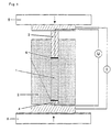
- the arrangement shown in FIG. 1 is selected for the resistance measurement.
- the ITO powder 1 is filled into a pressing device 5 equipped with a die 2 and an upper and a lower punch 3, 4, the upper and lower punch 3, 4 moving towards one another during the pressing process.
- the surfaces of the upper and lower punches 3, 4 are provided with gold contacts 6, which are connected to a current transmitter or a measuring transducer, so that at constant current, marked with the symbol 1 in FIG. 1, continuously during the compression of the ITO Powder 1 in the die 2 the voltage drop (symbolized by U in FIG. 1) can be measured across the compressed powder sample.
- the specific resistance is also determined with the arrangement according to FIG. 1 on a commercially available ITO powder.
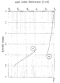
- the course of the specific electrical resistance over the density of the (curve 1) ITO powder according to the invention in comparison with that of a commercially available ITO powder (curve 2) is plotted in FIG.
- the values for the specific electrical resistance are plotted logarithmically.
- the measured value at a density of 3 g / cm 3 should be used as a comparison value for the specific electrical resistance. This corresponds to about 40% of the theoretical density (about 7.14 g / cm 3 ) of indium tin oxide.
- the ITO powder according to the invention shows a specific electrical resistance of 2 ⁇ cm and is therefore in its specific resistance about two orders of magnitude lower than that of the commercially available ITO powder.
- the ITO mixed crystal powder according to the invention which is qualified in this way, is hot isostatically pressed for 4 hours for further use in an evacuated capsule made of stainless steel at a pressure of 50 MPa and a temperature of 970 ° C.
- the "frozen" oxygen vacancies obtained as charge carriers by the manufacturing process according to the invention in the ITO mixed crystal powder remain largely present in the material in this sintering process (in contrast to pressureless sintering in an air atmosphere) and thus ensure a high charge carrier concentration in the target made from the powder, that after hot isostatic pressing, a plate (8 mm thick) is cut out of the sintering block and used in a magnetron sputtering system.
- an ITO layer is deposited on a glass substrate, which has a charge carrier concentration of 10.1 x 10 20 cm -3 .
- the charge carrier concentration of the ITO layer corresponds to that of the ITO mixed crystal powder according to the invention.
Landscapes
- Chemical & Material Sciences (AREA)
- Organic Chemistry (AREA)
- Inorganic Chemistry (AREA)
- Conductive Materials (AREA)
- Compositions Of Oxide Ceramics (AREA)
- Physical Vapour Deposition (AREA)
- Powder Metallurgy (AREA)
Description
Die elektrische Leitfähigkeit bzw. deren Kehrwert, der spezifische elektrische Widerstand, wird von folgenden Faktoren beeinflußt bzw. optimiert:
- Maximierung der Konzentration der elektrischen Ladungsträger durch "Einfrieren" der sich bei Schmelztemperatur im Gleichgewicht befindenden Anionenleerstellen.
- Gleichmäßige und vollständige Verteilung der Atome der zur Mobilität der Ladungsträger beitragenden Dotierungselemente im Mischkristallgitter.
- Hohe Dichte der durch die Kristallisation des erschmolzenen Oxids entstandenen einzelnen Mischkristallteilchen.
Anhand von diesen Berichten ist es klar, daß hohe Konzentrationen von Sauerstoffleerstellen und Elektronen-Donatoren im Indium-Oxid-Mischkristallgitter zu hohen elektrischen Leitfähigkeiten keiten bzw. niedrigem spezifischem Widerstand führen. Weiter ist festzustellen, daß die Konzentration der Sauerstoffleerstellen in einem oxidischen Mischkristall erhöht werden kann, wenn dieser als Festkörper einer möglichst hohen Temperatur ausgesetzt und dieser Zustand bei niedrigerer Temperatur stabilisiert wird, indem man rasch abgekühlt. Als möglichst hohe Temperatur ist hierbei eine Temperatur knapp unter dem Schmelzpunkt zu verstehen.
Das ITO-Pulver 1 wird in eine mit einer Matritze 2 und einem Ober- und einem Unterstempel 3,4 ausgestatteten Preßvorrichtung 5 gefüllt, wobei Ober- und Unterstempel 3,4 sich während des Preßvorgangs aufeinander zubewegen. Die Oberflächen des Ober- und des Unterstempels 3,4 sind mit Goldkontakten 6 versehen, die mit einem Stromgeber bzw. einem Meßumformer verbunden sind, so daß bei konstantem Strom, in der Figur 1 mit dem Symbol l gekennzeichnet, kontinuierlich während des Verdichtens des ITO-Pulvers 1 in der Matritze 2 der Spannungsabfall (in Figur 1 symbolisiert durch U) über der verdichteten Pulverprobe gemessen werden kann.
Im Vergleich zu dem erfindungsgemäßen, nach dem oben angeführten Beispiel hergestellten ITO-Pulver wird ebenfalls mit der Anordnung gemäß Figur 1 an einem marktüblichen ITO-Pulver der spezifische Widerstand ermittelt.
Der Verlauf des spezifischen elektrischen Widerstands über der Dichte des erfindungsgemäßen (Kurve 1) ITO-Pulvers im Vergleich mit dem eines marktüblichen ITO-Pulvers (Kurve 2) sind in Figur 2 aufgetragen. Die Werte für den spezifischen elektrischen Widerstand sind logarithmisch aufgetragen. Als Vergleichswert für den spezifischen elektrischen Widerstand soll der Meßwert bei einer Dichte von 3 g/cm3 herangezogen werden. Dies entspricht etwa 40 % theoretischer Dichte (ca.7,14 g/cm3) von Indium-Zinn-Oxid. Das erfindungsgemäße ITO-Pulver zeigt hier einen spezifischen elektrischen Widerstand von 2 Ω cm und liegt damit in seinem spezifischen Widerstand um etwa zwei Zehnerpotenzen unter dem des marktüblichen ITO-Pulvers.
Claims (9)
- Verfahren zur Herstellung eines Mischkristallpulvers mit einem elektrischem Widerstand kleiner 100 Ωcm durch die Reaktion mindestens zweier Reaktionspartner in einem Plasmalichtbogen einer eine Einfüllöffnung für die Reaktionspartner und eine Auslaßöffnung mit einer Gaszuführvorrichtung aufweisenden Plasmakammer zu einem schmelzflüssigen Material, wobei als erster Reaktionspartner eine schmelzflüssige Indium-Zinn-Legierung und als zweiter Reaktionspartner ein Gas verwendet werden, dadurch gekennzeichnet, daß das im Plasmalichtbogen reagierte Material an der Auslaßöffnung der Plasmakammer mit einem Gasstrom beaufschlagt wird, der das Material mit einer Abkühlrate im Bereich von 105 K/s bis 108 K/s auf eine Temperatur zwischen 50°C und 400°C abkühlt, wobei ein Indium-Zinn-Oxid Mischkristallpulver gebildet wird.
- Verfahren zur Herstellung eines Mischkristallpulvers nach Anspruch 1 , dadurch gekennzeichnet, daß die Abkühlrate vorzugsweise im Bereich von 106 K/s bis 108 K/s liegt.
- Verfahren zur Herstellung eines Mischkristallpulvers nach Anspruch 1 oder 2, dadurch gekennzeichnet, daß der Gasstrom zur Abkühlung des Materials eine Geschwindigkeit zwischen 300 m/s und 500 m/s aufweist.
- Verfahren zur Herstellung eines Mischkristallpulvers nach einem der Ansprüche 1 bis 3, dadurch gekennzeichnet, daß als zweiter Reaktionspartner Sauerstoff verwendet wird und ein Indium-Zinn-Oxid Mischkristallpulver gebildet wird, das mindestens 90 Vol. % Indium-Zinn-Oxid Mischkristallphase im Kristallgitter von Indiumoxid aufweist.
- Mischkristallpulver aus Indium-Zinn-Oxid mit mindestens 90 Vol. % Indium-Zinn-Oxid Mischkristallphase im Kristallgitter von Indiumoxid , dadurch gekennzeichnet, daß das auf 35 % bis 50 % seiner theoretischen Dichte verdichtete Indium-Zinn-Oxid Mischkristallpulver einen spezifischen elektrischen Widerstand im Bereich von 0,01 Ωcm bis 95 Ωcm aufweist.
- Mischkristallpulver nach Anspruch 5 , dadurch gekennzeichnet, daß das auf 40 % seiner theoretischen Dichte verdichtete Indium-Zinn-Oxid Mischkristallpulver einen spezifischen elektrischen Widerstand im Bereich von 0,01 Ωcm bis 20 Ωcm aufweist.
- Mischkristallpulver nach Anspruch 5 oder 6 , dadurch gekennzeichnet, daß das Indium-Zinn-Oxid Mischkristallpulver eine Konzentration an elektrischen Ladungsträgern im Bereich von 5 x 10²⁰ bis 30 x 1020 cm-3 aufweist.
- Mischkristallpulver nach einem der Ansprüche 5 bis 7, dadurch gekennzeichnet, daß das Indium-Zinn-Oxid Mischkristallpulver eine spezifische Oberfläche nach Brunauer-Emmett-Teller (BET) von maximal 3 m2/g bei einer mittleren Primärteilchengröße im Bereich von 0,03 µm bis 0,2 µm aufweist.
- Verwendung des Mischkristallpulvers nach einem der Ansprüche 5 bis 8 zur Erzeugung von Indium-Zinn-Oxid Schichten.
Applications Claiming Priority (2)
| Application Number | Priority Date | Filing Date | Title |
|---|---|---|---|
| DE19721649A DE19721649C2 (de) | 1997-05-23 | 1997-05-23 | Verfahren zur Herstellung eines Mischkristallpulvers mit geringem spezifischen elektrischen Widerstand |
| DE19721649 | 1997-05-23 |
Publications (3)
| Publication Number | Publication Date |
|---|---|
| EP0879791A1 EP0879791A1 (de) | 1998-11-25 |
| EP0879791B1 true EP0879791B1 (de) | 2001-01-03 |
| EP0879791B2 EP0879791B2 (de) | 2005-10-12 |
Family
ID=7830313
Family Applications (1)
| Application Number | Title | Priority Date | Filing Date |
|---|---|---|---|
| EP98104890A Expired - Lifetime EP0879791B2 (de) | 1997-05-23 | 1998-03-18 | Verfahren zur Herstellung eines ITO-Mischkristallpulvers mit geringem elektrischem Widerstand |
Country Status (9)
| Country | Link |
|---|---|
| US (1) | US6030507A (de) |
| EP (1) | EP0879791B2 (de) |
| JP (1) | JP2888340B2 (de) |
| KR (1) | KR100289183B1 (de) |
| CN (1) | CN1082492C (de) |
| DE (2) | DE19721649C2 (de) |
| MY (1) | MY118715A (de) |
| SG (1) | SG66906A1 (de) |
| TW (1) | TW501958B (de) |
Families Citing this family (13)
| Publication number | Priority date | Publication date | Assignee | Title |
|---|---|---|---|---|
| JP2000319017A (ja) * | 1999-04-30 | 2000-11-21 | Japan Science & Technology Corp | 空格子点に位置および濃度制御してドーパントを導入した化合物 |
| FR2839506B1 (fr) * | 2002-05-10 | 2005-06-10 | Michelle Paparone Serole | Oxyde mixte d'indium etain dit ito a grande conductivite electrique a nanostructure |
| US7601661B2 (en) * | 2003-12-25 | 2009-10-13 | Mitsui Mining & Smelting Co., Ltd. | Indium oxide-tin oxide powder and sputtering target using the same |
| FR2887162B1 (fr) * | 2005-06-20 | 2008-08-29 | Bernard Serole | Procede de fabrication de metaux, alliages metalliques, composites et hybrides amorphes et a nano structure |
| KR101092520B1 (ko) | 2009-11-24 | 2011-12-13 | 인하대학교 산학협력단 | 열플라즈마를 이용한 인듐-주석 산화물 나노분말의 제조방법 |
| EP2841630B1 (de) * | 2012-04-24 | 2017-04-12 | Forschungsverbund Berlin E.V. | Verfahren und vorrichtung zum züchten von indiumoxid (in203)-einkristallen und indiumoxid (in203)-einkristall |
| JP5924214B2 (ja) * | 2012-09-27 | 2016-05-25 | 三菱マテリアル株式会社 | Ito粉末及びその製造方法 |
| JP6788773B2 (ja) * | 2016-09-21 | 2020-11-25 | パナソニックIpマネジメント株式会社 | 抵抗測定装置とその方法 |
| CN107946013B (zh) * | 2017-11-27 | 2019-06-07 | 江民德 | 一种钕铁硼复合磁性材料的生产工艺 |
| JP7411501B2 (ja) * | 2020-05-13 | 2024-01-11 | 日東精工アナリテック株式会社 | 粉体の抵抗率測定装置および抵抗率測定方法 |
| CN112479682A (zh) * | 2020-12-15 | 2021-03-12 | 株洲火炬安泰新材料有限公司 | 一种环保高效ito靶材的制备方法 |
| CN113321238A (zh) * | 2021-06-04 | 2021-08-31 | 昆明理工大学 | 一种纳米ito粉末的制备方法 |
| CN117263232B (zh) * | 2023-06-13 | 2025-08-19 | 昆明理工大学 | 一种ito纳米线复合材料的制备方法 |
Family Cites Families (15)
| Publication number | Priority date | Publication date | Assignee | Title |
|---|---|---|---|---|
| JPS6120004A (ja) * | 1984-07-09 | 1986-01-28 | Sumitomo Electric Ind Ltd | イメ−ジフアイバ接続部の構造 |
| JPS6227533A (ja) * | 1985-07-26 | 1987-02-05 | Japan Synthetic Rubber Co Ltd | 内部酸化型合金およびその成形物の製造方法 |
| US5071800A (en) * | 1989-02-28 | 1991-12-10 | Tosoh Corporation | Oxide powder, sintered body, process for preparation thereof and targe composed thereof |
| DE4023278A1 (de) * | 1990-07-21 | 1992-01-23 | Messer Griesheim Gmbh | Verfahren und vorrichtung zur herstellung von metalloxidpulvern |
| JPH04281840A (ja) * | 1991-03-07 | 1992-10-07 | Takeshi Masumoto | 金属酸化物超微粒子の製造方法及び製造装置 |
| JPH04293767A (ja) * | 1991-03-22 | 1992-10-19 | Ulvac Japan Ltd | 透明導電膜の製造方法およびその製造装置 |
| JP3232591B2 (ja) † | 1991-07-22 | 2001-11-26 | 住友金属鉱山株式会社 | 酸化インジウム−酸化錫微粉末及びその製造方法 |
| EP0584672B1 (de) * | 1992-08-19 | 1996-06-12 | Tosoh Corporation | Verfahren zur Herstellung eines Indiumoxidpulvers verwendbar für einen ITO-Sinterkörper mit hoher Dichte |
| AU3495595A (en) * | 1994-08-25 | 1996-03-22 | Qqc, Inc. | Nanoscale particles, and uses for same |
| FR2724123A1 (fr) * | 1994-09-07 | 1996-03-08 | Serole Bernard | Dispositif permettant la stabilisation d'une reaction chimique continue entre plusieurs corps dans un plasma |
| US5580641A (en) * | 1995-05-25 | 1996-12-03 | Lockheed Martin Energy Systems, Inc. | Method of forming electrical pathways in indium-tin-oxide coatings |
| EP0761838B1 (de) * | 1995-08-18 | 2001-08-08 | W.C. Heraeus GmbH & Co. KG | Target für die Kathodenzerstäubung und Verfahren zur Herstellung eines solchen Targets |
| DE19540379C1 (de) * | 1995-08-18 | 1996-09-26 | Heraeus Gmbh W C | Target für die Kathodenzerstäubung und Verfahren zur Herstellung eines solchen Targets |
| JP3734540B2 (ja) * | 1995-10-13 | 2006-01-11 | 三井金属鉱業株式会社 | 酸化インジウム−酸化亜鉛系焼結体ターゲットの製造方法 |
| US5866493A (en) * | 1995-11-30 | 1999-02-02 | Korea Academy Of Industrial Technology | Method of manufacturing a sintered body of indium tin oxide |
-
1997
- 1997-05-23 DE DE19721649A patent/DE19721649C2/de not_active Expired - Fee Related
-
1998
- 1998-03-18 EP EP98104890A patent/EP0879791B2/de not_active Expired - Lifetime
- 1998-03-18 DE DE59800413T patent/DE59800413D1/de not_active Expired - Lifetime
- 1998-05-13 TW TW087107365A patent/TW501958B/zh not_active IP Right Cessation
- 1998-05-14 US US09/078,947 patent/US6030507A/en not_active Expired - Fee Related
- 1998-05-18 SG SG1998001239A patent/SG66906A1/en unknown
- 1998-05-21 MY MYPI98002270A patent/MY118715A/en unknown
- 1998-05-22 JP JP10141285A patent/JP2888340B2/ja not_active Expired - Fee Related
- 1998-05-22 CN CN98102907A patent/CN1082492C/zh not_active Expired - Fee Related
- 1998-05-22 KR KR1019980018486A patent/KR100289183B1/ko not_active Expired - Fee Related
Also Published As
| Publication number | Publication date |
|---|---|
| DE19721649C2 (de) | 2003-02-20 |
| JPH1111946A (ja) | 1999-01-19 |
| EP0879791B2 (de) | 2005-10-12 |
| KR100289183B1 (ko) | 2001-06-01 |
| KR19980087288A (ko) | 1998-12-05 |
| US6030507A (en) | 2000-02-29 |
| TW501958B (en) | 2002-09-11 |
| DE19721649A1 (de) | 1998-11-26 |
| EP0879791A1 (de) | 1998-11-25 |
| SG66906A1 (en) | 2000-01-25 |
| CN1082492C (zh) | 2002-04-10 |
| JP2888340B2 (ja) | 1999-05-10 |
| DE59800413D1 (de) | 2001-02-08 |
| MY118715A (en) | 2005-01-31 |
| CN1208018A (zh) | 1999-02-17 |
Similar Documents
| Publication | Publication Date | Title |
|---|---|---|
| DE69414235T2 (de) | Schichtstrukturoxyd | |
| DE69417475T2 (de) | Herstellung von Silber/Vanadiumoxidkathoden | |
| DE69132176T2 (de) | Verfahren zur Herstellung von Elektroden | |
| DE3853961T2 (de) | Verfahren zur Herstellung eines supraleitenden Drahts. | |
| EP0879791B2 (de) | Verfahren zur Herstellung eines ITO-Mischkristallpulvers mit geringem elektrischem Widerstand | |
| DE69720640T2 (de) | Lithium-Ionen leitende Glaskeramiken und damit hergestellte elektrische Zellen und Glassensoren | |
| DE69823042T2 (de) | Varistoren auf basis von durch mechanische zerkleinerung hergestellten nanokristallpulvern | |
| DE69611642T2 (de) | Zinkoxidkeramik, Verfahren zu deren Herstellung und Zinkoxidvaristoren | |
| DE69032065T2 (de) | Verbundwerkstoff von Silber und Metalloxyd und Verfahren zur Herstellung desselben | |
| DE4407774C1 (de) | Target für die Kathodenzerstäubung zur Herstellung transparenter, leitfähiger Schichten und Verfahren zu seiner Herstellung | |
| DE3781956T2 (de) | Verfahren zur herstellung eines ag-metalloxid-material fuer elektrische kontakte. | |
| DE112021007772T5 (de) | Ionenleitender feststoff und feststoffbatterie | |
| DE69024244T4 (de) | Verfahren zur Herstellung von supraleitendem Material auf Bismuth-Basis | |
| DE68919299T2 (de) | Sinterkörper aus Zinkoxid und seine Herstellung. | |
| EP1501759A1 (de) | Verfahren zur herstellung eines metalloxidpulvers oder eines halbleiteroxidpulvers, oxidpulver, festk rper und seine verwendu ng | |
| DE69017556T2 (de) | Thermoelektrisches Fe-Silizid-Konversionsmaterial vom P-Typ. | |
| DE69016833T2 (de) | Verfahren zum Herstellen von Molybdän-Platinoxyd-Elektroden für thermoelektrische Generatoren. | |
| EP1157429A1 (de) | Supraleitende körper aus zinkdotiertem kupferoxidmaterial | |
| DE112021007743T5 (de) | Ionenleitfähiger feststoff und feststoffbatterie | |
| DE112021007747T5 (de) | Ionenleitender feststoff und feststoffbatterie | |
| DE68919836T2 (de) | Methode zur Herstellung eines supraleitenden Kabels und Drahtes. | |
| DE69110504T2 (de) | Verfahren zur Herstellung eines mit einer metallischen Schutzschicht versehenen supraleitenden Drahtes aus Keramik. | |
| DE2811044C3 (de) | Piezoelektrische kristalline Filme | |
| DE69010776T2 (de) | Dielektrische Keramik und Verfahren zu deren Herstellung. | |
| US5700418A (en) | Method of manufacture of components made of sintered indium-tin-oxide solid-solution crystals |
Legal Events
| Date | Code | Title | Description |
|---|---|---|---|
| PUAI | Public reference made under article 153(3) epc to a published international application that has entered the european phase |
Free format text: ORIGINAL CODE: 0009012 |
|
| 17P | Request for examination filed |
Effective date: 19980324 |
|
| AK | Designated contracting states |
Kind code of ref document: A1 Designated state(s): BE CH DE FR GB IT LI NL |
|
| AX | Request for extension of the european patent |
Free format text: AL;LT;LV;MK;RO;SI |
|
| RAP1 | Party data changed (applicant data changed or rights of an application transferred) |
Owner name: W.C. HERAEUS GMBH & CO. KG |
|
| AKX | Designation fees paid |
Free format text: BE CH DE FR GB IT LI NL |
|
| 17Q | First examination report despatched |
Effective date: 19991111 |
|
| RTI1 | Title (correction) |
Free format text: PROCESS FOR THE PREPARATION OF ITO MIXED CRYSTALLINE POWDER WITH LOW ELECTRIC RESISTANCE |
|
| GRAG | Despatch of communication of intention to grant |
Free format text: ORIGINAL CODE: EPIDOS AGRA |
|
| GRAG | Despatch of communication of intention to grant |
Free format text: ORIGINAL CODE: EPIDOS AGRA |
|
| GRAH | Despatch of communication of intention to grant a patent |
Free format text: ORIGINAL CODE: EPIDOS IGRA |
|
| GRAH | Despatch of communication of intention to grant a patent |
Free format text: ORIGINAL CODE: EPIDOS IGRA |
|
| GRAA | (expected) grant |
Free format text: ORIGINAL CODE: 0009210 |
|
| AK | Designated contracting states |
Kind code of ref document: B1 Designated state(s): BE CH DE FR GB IT LI NL |
|
| REG | Reference to a national code |
Ref country code: CH Ref legal event code: NV Representative=s name: KIRKER & CIE SA Ref country code: CH Ref legal event code: EP |
|
| GBT | Gb: translation of ep patent filed (gb section 77(6)(a)/1977) |
Effective date: 20010103 |
|
| REF | Corresponds to: |
Ref document number: 59800413 Country of ref document: DE Date of ref document: 20010208 |
|
| ITF | It: translation for a ep patent filed | ||
| ET | Fr: translation filed | ||
| PLBQ | Unpublished change to opponent data |
Free format text: ORIGINAL CODE: EPIDOS OPPO |
|
| PLBI | Opposition filed |
Free format text: ORIGINAL CODE: 0009260 |
|
| PLBF | Reply of patent proprietor to notice(s) of opposition |
Free format text: ORIGINAL CODE: EPIDOS OBSO |
|
| 26 | Opposition filed |
Opponent name: SUMITOMO CHEMICAL CO., LTD. Effective date: 20011002 |
|
| REG | Reference to a national code |
Ref country code: GB Ref legal event code: IF02 |
|
| NLR1 | Nl: opposition has been filed with the epo |
Opponent name: SUMITOMO CHEMICAL CO., LTD. |
|
| PGFP | Annual fee paid to national office [announced via postgrant information from national office to epo] |
Ref country code: CH Payment date: 20020225 Year of fee payment: 5 |
|
| PLBF | Reply of patent proprietor to notice(s) of opposition |
Free format text: ORIGINAL CODE: EPIDOS OBSO |
|
| PLAW | Interlocutory decision in opposition |
Free format text: ORIGINAL CODE: EPIDOS IDOP |
|
| PGFP | Annual fee paid to national office [announced via postgrant information from national office to epo] |
Ref country code: GB Payment date: 20030226 Year of fee payment: 6 |
|
| PGFP | Annual fee paid to national office [announced via postgrant information from national office to epo] |
Ref country code: NL Payment date: 20030228 Year of fee payment: 6 |
|
| PG25 | Lapsed in a contracting state [announced via postgrant information from national office to epo] |
Ref country code: LI Free format text: LAPSE BECAUSE OF NON-PAYMENT OF DUE FEES Effective date: 20030331 Ref country code: CH Free format text: LAPSE BECAUSE OF NON-PAYMENT OF DUE FEES Effective date: 20030331 |
|
| RTI2 | Title (correction) |
Free format text: PROCESS FOR THE PREPARATION OF ITO MIXED CRYSTALLINE POWDER WITH LOW ELECTRIC RESISTANCE |
|
| APAC | Appeal dossier modified |
Free format text: ORIGINAL CODE: EPIDOS NOAPO |
|
| APBQ | Date of receipt of statement of grounds of appeal recorded |
Free format text: ORIGINAL CODE: EPIDOSNNOA3O |
|
| REG | Reference to a national code |
Ref country code: CH Ref legal event code: PL |
|
| PG25 | Lapsed in a contracting state [announced via postgrant information from national office to epo] |
Ref country code: GB Free format text: LAPSE BECAUSE OF NON-PAYMENT OF DUE FEES Effective date: 20040318 |
|
| PG25 | Lapsed in a contracting state [announced via postgrant information from national office to epo] |
Ref country code: NL Free format text: LAPSE BECAUSE OF NON-PAYMENT OF DUE FEES Effective date: 20041001 |
|
| GBPC | Gb: european patent ceased through non-payment of renewal fee |
Effective date: 20040318 |
|
| NLV4 | Nl: lapsed or anulled due to non-payment of the annual fee |
Effective date: 20041001 |
|
| APAA | Appeal reference recorded |
Free format text: ORIGINAL CODE: EPIDOS REFN |
|
| PG25 | Lapsed in a contracting state [announced via postgrant information from national office to epo] |
Ref country code: IT Free format text: LAPSE BECAUSE OF NON-PAYMENT OF DUE FEES Effective date: 20050318 |
|
| PLAQ | Examination of admissibility of opposition: information related to despatch of communication + time limit deleted |
Free format text: ORIGINAL CODE: EPIDOSDOPE2 |
|
| PLAR | Examination of admissibility of opposition: information related to receipt of reply deleted |
Free format text: ORIGINAL CODE: EPIDOSDOPE4 |
|
| PLBQ | Unpublished change to opponent data |
Free format text: ORIGINAL CODE: EPIDOS OPPO |
|
| PLAB | Opposition data, opponent's data or that of the opponent's representative modified |
Free format text: ORIGINAL CODE: 0009299OPPO |
|
| PLBP | Opposition withdrawn |
Free format text: ORIGINAL CODE: 0009264 |
|
| APBU | Appeal procedure closed |
Free format text: ORIGINAL CODE: EPIDOSNNOA9O |
|
| RAP2 | Party data changed (patent owner data changed or rights of a patent transferred) |
Owner name: W.C. HERAEUS GMBH |
|
| PUAH | Patent maintained in amended form |
Free format text: ORIGINAL CODE: 0009272 |
|
| STAA | Information on the status of an ep patent application or granted ep patent |
Free format text: STATUS: PATENT MAINTAINED AS AMENDED |
|
| APAH | Appeal reference modified |
Free format text: ORIGINAL CODE: EPIDOSCREFNO |
|
| 27A | Patent maintained in amended form |
Effective date: 20051012 |
|
| AK | Designated contracting states |
Kind code of ref document: B2 Designated state(s): BE CH DE FR GB IT LI NL |
|
| ET3 | Fr: translation filed ** decision concerning opposition | ||
| PGFP | Annual fee paid to national office [announced via postgrant information from national office to epo] |
Ref country code: BE Payment date: 20090430 Year of fee payment: 12 |
|
| PGFP | Annual fee paid to national office [announced via postgrant information from national office to epo] |
Ref country code: FR Payment date: 20090312 Year of fee payment: 12 |
|
| PGFP | Annual fee paid to national office [announced via postgrant information from national office to epo] |
Ref country code: DE Payment date: 20100324 Year of fee payment: 13 |
|
| BERE | Be: lapsed |
Owner name: W.C. *HERAEUS G.M.B.H. Effective date: 20100331 |
|
| REG | Reference to a national code |
Ref country code: FR Ref legal event code: ST Effective date: 20101130 |
|
| PG25 | Lapsed in a contracting state [announced via postgrant information from national office to epo] |
Ref country code: FR Free format text: LAPSE BECAUSE OF NON-PAYMENT OF DUE FEES Effective date: 20100331 |
|
| PG25 | Lapsed in a contracting state [announced via postgrant information from national office to epo] |
Ref country code: BE Free format text: LAPSE BECAUSE OF NON-PAYMENT OF DUE FEES Effective date: 20100331 |
|
| PG25 | Lapsed in a contracting state [announced via postgrant information from national office to epo] |
Ref country code: DE Free format text: LAPSE BECAUSE OF NON-PAYMENT OF DUE FEES Effective date: 20111001 |
|
| REG | Reference to a national code |
Ref country code: DE Ref legal event code: R119 Ref document number: 59800413 Country of ref document: DE Effective date: 20111001 |