EP0871052B1 - Konfokales Mikroskop mit einem motorischen Scanningtisch - Google Patents
Konfokales Mikroskop mit einem motorischen Scanningtisch Download PDFInfo
- Publication number
- EP0871052B1 EP0871052B1 EP98105816A EP98105816A EP0871052B1 EP 0871052 B1 EP0871052 B1 EP 0871052B1 EP 98105816 A EP98105816 A EP 98105816A EP 98105816 A EP98105816 A EP 98105816A EP 0871052 B1 EP0871052 B1 EP 0871052B1
- Authority
- EP
- European Patent Office
- Prior art keywords
- array
- confocal microscope
- sensor
- microscope according
- diaphragm
- Prior art date
- Legal status (The legal status is an assumption and is not a legal conclusion. Google has not performed a legal analysis and makes no representation as to the accuracy of the status listed.)
- Expired - Lifetime
Links
- 238000003491 array Methods 0.000 claims description 16
- 230000003287 optical effect Effects 0.000 claims description 16
- QNRATNLHPGXHMA-XZHTYLCXSA-N (r)-(6-ethoxyquinolin-4-yl)-[(2s,4s,5r)-5-ethyl-1-azabicyclo[2.2.2]octan-2-yl]methanol;hydrochloride Chemical compound Cl.C([C@H]([C@H](C1)CC)C2)CN1[C@@H]2[C@H](O)C1=CC=NC2=CC=C(OCC)C=C21 QNRATNLHPGXHMA-XZHTYLCXSA-N 0.000 claims description 4
- 238000006073 displacement reaction Methods 0.000 claims 2
- 230000000694 effects Effects 0.000 claims 1
- 238000005286 illumination Methods 0.000 description 12
- 238000012545 processing Methods 0.000 description 7
- 238000001514 detection method Methods 0.000 description 6
- 238000007689 inspection Methods 0.000 description 6
- 230000010287 polarization Effects 0.000 description 6
- 238000010586 diagram Methods 0.000 description 5
- 238000004519 manufacturing process Methods 0.000 description 5
- 238000005259 measurement Methods 0.000 description 5
- 238000001914 filtration Methods 0.000 description 4
- 238000013507 mapping Methods 0.000 description 4
- 239000004065 semiconductor Substances 0.000 description 4
- 238000011144 upstream manufacturing Methods 0.000 description 4
- 230000008859 change Effects 0.000 description 3
- 238000003384 imaging method Methods 0.000 description 3
- 230000001360 synchronised effect Effects 0.000 description 3
- 231100000716 Acceptable daily intake Toxicity 0.000 description 2
- 230000001133 acceleration Effects 0.000 description 2
- 230000001419 dependent effect Effects 0.000 description 2
- 239000004744 fabric Substances 0.000 description 2
- 239000000835 fiber Substances 0.000 description 2
- 230000006872 improvement Effects 0.000 description 2
- 230000010354 integration Effects 0.000 description 2
- 230000015654 memory Effects 0.000 description 2
- 230000005855 radiation Effects 0.000 description 2
- 206010034960 Photophobia Diseases 0.000 description 1
- 230000003321 amplification Effects 0.000 description 1
- 230000002457 bidirectional effect Effects 0.000 description 1
- 230000005540 biological transmission Effects 0.000 description 1
- 230000015572 biosynthetic process Effects 0.000 description 1
- 230000001276 controlling effect Effects 0.000 description 1
- 238000013500 data storage Methods 0.000 description 1
- 230000007547 defect Effects 0.000 description 1
- 230000001934 delay Effects 0.000 description 1
- 238000013461 design Methods 0.000 description 1
- 208000013469 light sensitivity Diseases 0.000 description 1
- 238000013508 migration Methods 0.000 description 1
- 230000005012 migration Effects 0.000 description 1
- 238000003199 nucleic acid amplification method Methods 0.000 description 1
- 239000013307 optical fiber Substances 0.000 description 1
- 239000002245 particle Substances 0.000 description 1
- 230000010363 phase shift Effects 0.000 description 1
- 230000001105 regulatory effect Effects 0.000 description 1
- 230000035945 sensitivity Effects 0.000 description 1
- 230000009897 systematic effect Effects 0.000 description 1
- 238000012546 transfer Methods 0.000 description 1
Images



Classifications
-
- G—PHYSICS
- G02—OPTICS
- G02B—OPTICAL ELEMENTS, SYSTEMS OR APPARATUS
- G02B21/00—Microscopes
- G02B21/0004—Microscopes specially adapted for specific applications
- G02B21/002—Scanning microscopes
- G02B21/0024—Confocal scanning microscopes (CSOMs) or confocal "macroscopes"; Accessories which are not restricted to use with CSOMs, e.g. sample holders
- G02B21/0052—Optical details of the image generation
- G02B21/0068—Optical details of the image generation arrangements using polarisation
-
- G—PHYSICS
- G02—OPTICS
- G02B—OPTICAL ELEMENTS, SYSTEMS OR APPARATUS
- G02B21/00—Microscopes
- G02B21/0004—Microscopes specially adapted for specific applications
- G02B21/002—Scanning microscopes
- G02B21/0024—Confocal scanning microscopes (CSOMs) or confocal "macroscopes"; Accessories which are not restricted to use with CSOMs, e.g. sample holders
- G02B21/0036—Scanning details, e.g. scanning stages
-
- G—PHYSICS
- G02—OPTICS
- G02B—OPTICAL ELEMENTS, SYSTEMS OR APPARATUS
- G02B21/00—Microscopes
- G02B21/0004—Microscopes specially adapted for specific applications
- G02B21/002—Scanning microscopes
- G02B21/0024—Confocal scanning microscopes (CSOMs) or confocal "macroscopes"; Accessories which are not restricted to use with CSOMs, e.g. sample holders
- G02B21/0036—Scanning details, e.g. scanning stages
- G02B21/004—Scanning details, e.g. scanning stages fixed arrays, e.g. switchable aperture arrays
-
- G—PHYSICS
- G02—OPTICS
- G02B—OPTICAL ELEMENTS, SYSTEMS OR APPARATUS
- G02B21/00—Microscopes
- G02B21/0004—Microscopes specially adapted for specific applications
- G02B21/002—Scanning microscopes
- G02B21/0024—Confocal scanning microscopes (CSOMs) or confocal "macroscopes"; Accessories which are not restricted to use with CSOMs, e.g. sample holders
- G02B21/0052—Optical details of the image generation
- G02B21/0056—Optical details of the image generation based on optical coherence, e.g. phase-contrast arrangements, interference arrangements
-
- G—PHYSICS
- G02—OPTICS
- G02B—OPTICAL ELEMENTS, SYSTEMS OR APPARATUS
- G02B21/00—Microscopes
- G02B21/0004—Microscopes specially adapted for specific applications
- G02B21/002—Scanning microscopes
- G02B21/0024—Confocal scanning microscopes (CSOMs) or confocal "macroscopes"; Accessories which are not restricted to use with CSOMs, e.g. sample holders
- G02B21/0052—Optical details of the image generation
- G02B21/0072—Optical details of the image generation details concerning resolution or correction, including general design of CSOM objectives
-
- G—PHYSICS
- G02—OPTICS
- G02B—OPTICAL ELEMENTS, SYSTEMS OR APPARATUS
- G02B21/00—Microscopes
- G02B21/0004—Microscopes specially adapted for specific applications
- G02B21/002—Scanning microscopes
- G02B21/0024—Confocal scanning microscopes (CSOMs) or confocal "macroscopes"; Accessories which are not restricted to use with CSOMs, e.g. sample holders
- G02B21/008—Details of detection or image processing, including general computer control
Definitions
- a confocal microscope with a motorized scanning table to move a sample perpendicular to the optical axis of the Microscope is known from US 5 239 178.
- the microscope also has a light source array in a to the focal plane with a conjugate lens and a detector array a large number of photosensitive elements also in one plane conjugate to the focal plane of the microscope objective.
- the movement of the sample perpendicular to the optical axis of the Microscope takes place primarily in this confocal microscope microscopic area to the otherwise by the grid spacing vertical resolution of the light source array to increase to the optical axis.
- a detection of large object fields that are much larger than is the field of view of the lens transmitted in an image only possible to a limited extent with this confocal microscope. It need to take series of individual pictures of the object between which the object is in each case one of the image field diameter corresponding distance must be moved.
- A, but not confocal, nominal microscope that is used for Recording and saving of corresponding picture series is designed, for example, in EP 0 444 450-A1 described. Since this nomaric microscope is not confocal, it has only a low resolution towards the optical Axis on. In addition, this microscope is too slow, when the image information captures a large number of frames must become.
- the detection of large object fields in the shortest possible time but at the same time high resolution is with inspection devices, which in the manufacturing process, for example in the Semiconductor industry or used in the LCD manufacturing become mandatory.
- the present invention is intended to provide an arrangement for the optical inspection of semiconductors in the manufacturing process can be used. With this arrangement, both adequate resolution in the direction as well as perpendicular to the optical axis can be achieved. At the same time, big ones Image fields can be captured in the shortest possible time.
- the arrangement according to the invention is a confocal microscope a motorized scanning table to move the sample vertically to the optical axis of the microscope. It has an aperture array with a variety of translucent areas, so-called Pinholes, in one to the focal plane of the microscope objective conjugate level.
- the aperture array is a sensor array with a variety of photosensitive elements. Each light-sensitive element has a charge storage assigned.
- the sensor array has a device for Moving the charges stored in the charge stores from one store to another store like this for example, the case with the so-called TDI sensors.
- a synchronization unit is provided, which a shifting of the charges according to the movement of the Pixel of a sample point in the plane of the sensor array causes.
- the for confocal microscopes Due to the confocal microscopic arrangement, the for confocal microscopes usual high resolution both in the direction the optical axis as well as perpendicular to the optical axis achieved.
- a strongly magnifying Lens for example a lens with 20 to 120 times Magnification
- achievable resolution is for semiconductor inspection sufficient.
- By using an aperture array and the associated large number of parallel ones confocal beam paths become one of the at any time Number of pinholes in the panel array corresponding number Object positions recorded.
- the movement of the image point of an object point takes place Measurement while moving the sample.
- the movement of the sample is preferably carried out along linear paths that are over the entire length of the sample in the direction of movement extend.
- the parallel confocal beam paths is a light source array that is a variety of each other has spaced light sources in a to the focal plane of the Objective conjugate plane arranged.
- the positions of the individual light sources are related to the positions of the translucent areas of the aperture array conjugate.
- Corresponding light source arrays are different Way feasible.
- the simplest variant results from the aperture array in a common part of the lighting and Observation beam path is arranged and the aperture array is backlit. This simple arrangement has however, the disadvantage that a substantial proportion of the Illumination light on the back of the panel array reflected and thereby a strong on the sensor array Signal background generated.
- Such a strong signal background can be avoided in that two separate aperture arrays in the Illumination beam path and in the observation beam path or Measuring beam path are provided. That in the lighting beam path arranged aperture array will then turn backlit.
- a lens array be upstream.
- Illuminated aperture arrays can also be made from the light source array a laser diode array or array-shaped through the end faces arranged optical fibers can be realized.
- a diffractive element for use come.
- the aperture array is the Light source array and the sensor array to each other at rest. All three components are fixed to each other.
- the sensor array is preferably a two-dimensional array photosensitive elements and the photosensitive Charge storage associated with elements with a large number columns arranged parallel to each other.
- the column direction is defined by the direction in which the charges be moved between the charge stores.
- Light source array and aperture array on the one hand and sensor array on the other should be arranged relative to each other so that each of the at least one translucent column arranged parallel to each other Area of the diaphragm array is shown.
- TDI sensors can be used as corresponding sensor arrays come. As far as such TDI sensors are light-insensitive areas between the photosensitive surfaces, they can so arranged and the figure between aperture array and Sensor be chosen so that the translucent areas of the Aperture arrays only on the photosensitive Areas are mapped.
- the translucent areas of the panel array are like this according to the direction of movement of the scanning table and the Image relationship between the object plane and the aperture array trained that the orbits of the images of all translucent Areas, while maintaining confocal filtering, one Fill part of the focal plane tightly, preferably without gaps.
- the image information for a strip whose Width the width of the perpendicular to the one-dimensional Direction of movement of the image section captured by the sensor array corresponds to completely confocal, without micro-movements perpendicular to the direction of movement are required.
- the translucent areas of the panel array can do this arranged in the form of a two-dimensional rhombic grid his. The center of every translucent area corresponds to the position of the theoretical grid point.
- the arrangement of the translucent is particularly advantageous Areas of the diaphragm array in the form of a rectangular grid, the grid axes of which are opposite to the linear direction of movement of the scanning table are rotated.
- a rectangular geometry offers advantages if that Light source array in the form of fiber lighting, one Lens arrays or as a corresponding lighting generating diffractive element is formed.
- Such an offset arrangement of several two-dimensional sensor arrays points at anamorphic Mapping of the aperture array onto the sensor array versus one Arrangement of a single sensor array with the same number photosensitive elements by the number of two-dimensional Arrays larger field of view, creating a results in a correspondingly larger signal / noise ratio.
- the invention is a single diaphragm array (4) with a large number transparent areas or holes in the common part of the Illumination and observation beam path arranged. It thereby forms the aperture array for the Detection beam path and the light source array for the Illumination of the object (8).
- the aperture array (4) is included via a light source (1) with a downstream condenser (2) Illuminated uniformly from the back. Everyone transparent area or each pinhole of the panel array (4) thereby forms a secondary light source.
- FIG. 1a To map the aperture array (4) to that on the motor Scanning table (9) positioned object (8) is the aperture array (4) a tube lens (5) with a microscope objective (7) downstream.
- the microscope objective (7) is shown in FIG. 1a shown in a highly simplified form as a single lens.
- the microscope lens (7) is infinite on focal length, i.e. on one Corrected infinite image spacing. This fact is in 1a indicated by the telecentric aperture (6).
- the aperture array (4), and with it the aperture array (4) formed light source array is over the tube lens (5) and the telecentric image confocal to the focal plane of the Objective (7) arranged. In the focal plane of the lens (7) this creates a lighting pattern that matches the image of the Aperture arrays (4) corresponds. This turns object (8) on to the transparent areas of the panel array (4) conjugate areas illuminated. The scattered on the object (8) or reflected light is from the lens (7) with the downstream Back tube lens (5) back onto the diaphragm array (4) shown.
- the aperture array (4) the confocal filtering with the result that only such light through the transparent areas of the aperture array (4) can transmit that in to the transparent Areas of the diaphragm array (4) confocal areas of the object (8) was scattered or reflected.
- a divider mirror between the aperture array (4) and the condenser (2) (3) through which a part of the object (8) scattered or reflected and through the aperture array (4) transmitted light in the direction of the sensor array (11) is mirrored.
- the mirrored beam path i.e. between the divider mirror (3) and sensor array (11) is one further imaging optics (10) are provided, through which the Iris array (4) is shown on the sensor array (11).
- TDI Sensor Time Delay and Integration
- Such a TDI Sensor has 2048 columns with 96 TDI stages each (rows) on.
- Each TDI stage in each column is a light sensitive Area and a charge storage assigned so that the number the pixels (photosensitive areas) and the charge storage Is 96 x 2048.
- the aperture array (4) has at least one number corresponding to the number of columns in the TDI sensor transparent areas so that on each column of the TDI Sensor at least one transparent area of the panel array (4) is shown.
- the complete scanning of the object field perpendicular to the Direction of movement of the scanning table (9) is carried out by a arrangement offset perpendicular to the direction of movement transparent areas.
- the charge shift in the sensor array corresponding to the Movement of the pixel of an object point becomes the whole Object field that corresponds to the line width of the sensor array, detected.
- Due to the staggered arrangement of the panels in the panel array are the paths of the pixels of the aperture in the Focal plane of the lens (7) close together without gaps. Therefore, no micro-shifts are perpendicular to the Direction of movement for complete detection of the image field required. This reduces the effort involved in data storage (Data sorting) and the tolerance requirements the movement of the scanning table.
- FIG. 1b these are the individual Components of the embodiment of Figure 1a corresponding components with the same reference numerals as in Figure 1a labeled.
- the differences to the embodiment 1a consist in that in FIG. 1b Aperture array (4b) downstream of the beam splitter (3 ') Observation or detection beam path is arranged. in the Illumination beam path is its own aperture array (4a) arranged that the light source array forms.
- the two Aperture arrays (4a) and (4b) are in relation to each other and to the focal plane the lens (7) arranged conjugate. Even the transparent ones Areas of the two diaphragm arrays (4a) and (4b) are in relation to one another conjugated.
- the beam splitter is on the object side (3 ') a lambda quarter plate (14) provided in known way causes the polarization of the light that transmitted twice through the lambda quarter plate (14) Is rotated 90 ° in polarization.
- Polarized light results from the use of a Polarization beam splitter (3 ') and a lambda quarter plate (14) a four times better utilization of the behind the Condenser (2) existing light compared to the embodiment according to Figure 1a.
- a corresponding arrangement of Polarization beam splitter, polarization filter and Lambda quarter plate is also in the embodiment possible with only one aperture array according to FIG. 1a.
- FIG. 3b shows a first exemplary embodiment of an aperture array (4, 4a, 4b).
- the aperture array (4) contains a number of translucent areas (4 1 - 4 20 ) corresponding to the number of pixels of the sensor (11), of which only 20 are shown in FIG. 3b for reasons of clarity.
- the distance between the next adjacent transparent areas is at least 4 times the diameter of the transparent areas.
- the transparent areas (4 1 - 4 20 ) form a two-dimensional rhombic grid, the angle between the two grid axes being selected such that the center is closest in each case, taking into account the imaging ratio between the diaphragm array (4, 4b) and the TDI sensor (11) neighboring transparent areas is mapped onto neighboring columns of the TDI sensor (11).
- This mapping assignment is shown in Figure 3c.
- Each square in FIG. 3c represents a light-sensitive area.
- the 96 stages are shown in the vertical direction and a section of the 2048 columns in the horizontal direction, the columns being designated by (P1-P4, P10, P11).
- the transparent area (4 1 ) is on the column (P1), the transparent area (4 2 ) on the column (P2), etc. on different columns of the TDI sensor (11) displayed.
- the transparent areas (4 1 - 4 10 ) are shown on different stages. Only the stage position on which the transparent area (4 11 ) is mapped corresponds again to the stage position of the area (4 1 ).
- FIG. 3a The image of the aperture array (4) and the TDI sensor (11) in the focal plane of the lens (7) and thus in a section plane of the object (8) is shown in Figure 3a.
- the Images of the translucent areas of the diaphragm array (4) are there with the same reference numerals as in FIG. 3b designated. Each square drawn there represents the picture the associated light-sensitive area of the TDI sensor (11).
- the linear direction of movement of the scanning table (9) the longer meander tracks are indicated by the arrow (S).
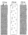
- FIGS. 4a to 4c show the same facts as in FIGS. 3a to 3c for an alternative aperture array (4 ') (see FIG. 4b).
- the transparent areas which correspond to those in FIG. 3b in terms of their diameter and their distance from the adjacent transparent area are arranged in such a way that a rectangular two-dimensional grid of transparent areas results.
- the grating axes of the right-angled grating are rotated with respect to the scanning direction (arrow (S)) such that, as in the previously described embodiment according to FIGS. 3a to 3c, a transparent area (4 1 , - 4 6 ,) is in each case a column of the TDI sensor (11) is shown.
- FIG. 4a shows the image of the diaphragm array (4 ') and the TDI sensor (11) in the focal plane of the lens (7).
- the light source array (4a) does not increase the light output only through a homogeneously illuminated panel array at the rear but through an aperture array with an upstream Lens array, a diffractive element or an upstream Fiber array for better illumination of the transparent areas of the panel array (4a) is formed. With sufficient punctiformity of the resulting secondary light sources can also be used on a lighting panel array (4a) to be dispensed with.
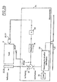
- the stage (9) consists essentially of the two table elements that can be moved in mutually perpendicular directions, the motor drives (20, 21), the Position measuring systems (22, 23) and a microcontroller (24).
- the object table (9) itself is for focusing in Can not be moved in the direction of the optical axis tripod shown.
- the two motor Drives (20, 21) for generating the movement in two orthogonal directions are preferably linear drives educated.
- the position measuring drives (22, 23), the Movement or deflection of the table (9) independently of one another in the two mutually perpendicular directions designed as a length measuring interferometer.
- This interferometer deliver when the table is moved in the direction of the Measuring beam path of the associated interferometer on a Radiation sensor has an irradiance that is a sinusoidal Dependence on the distance traveled. There is a period about the wavelength of the measuring light used in the associated Interferometer directly with the distance covered connected. Since the measurement signal is covered for longer periods If there are ambiguities in the way, there is also one Absolute calibration required by starting a measurement a zero position is approached. At any later time the current position in relation to this then results Zero position from the number of zero crossings of the Interferometer signal plus the phase difference of the detected sinusoidal signal in the calibration position and current position.
- the microcontroller (24) controls the drives (20, 21) of the Object table (9) according to the current position measurements, which are supplied by the measuring systems (22, 23) and by a host computer, not shown, via a bus line (29) certain target position values.
- the necessary one Control loop within the microcontroller (24) is in the figure 2b shown enlarged.
- the over the control bus For example, a CAN bus, data delivered is in a arithmetic logical unit (ALU) (33) in the current Converted target position values.
- ALU arithmetic logical unit
- the values determined in the ALU (33) become further ALUs (32) from the values supplied by the two measuring systems (22, 23) each subtracted so that the difference is the filing between Represents actual position and target position.
- This difference is in an integrator (34) integrated in time and subsequently in a unit (35) multiplied by a factor that Specifies amplification of the open control loop. That factor is usually negative by a phase shift of 180 ° cause.
- This amplified and time-integrated difference signal then sets the drive signal for the drives (20, 21) represents.
- the values of the current target positions in the two to each other vertical directions are simultaneously from the ALU (33) to another microcontroller via data lines (30, 31) (28), a driver (27) for reading out or clocking the TDI sensors (11) and image processing electronics (25) passed.
- Driver (27) causes a shift in the TDI sensor stored charges corresponding to the migration of a every pixel on the TDI sensor (11).
- the one from the TDI sensor (11) read charge data from an AD converter (26) digitized and subsequently also to the image processing electronics (25) passed on.
- the image processing electronics (25) receives the information for which table position those recorded with the TDI sensor Irradiations are entered in the image to be generated should.
- the electronics take into account the delays, due to the systematic properties of the TDI sensor caused. If the table is in one position located outside of the area to be recorded Range, the values given by the TDI sensor remain unconsidered.
- One of the image processing electronics is first Restoration of the recording performed. Doing so will be constant and compensates for linear errors caused, for example, by Changes in radiation intensity due to deviations in the Dimensions of the translucent areas within the Aperture arrays, table speed deviations from the Target speed or through different sensitivity characteristics the pixels of the TDI sensor arise can. Having such constant or linear errors are compensated for by suitable filtering Structures of the object, for example the exposed wafer be suppressed a bit to make mistakes between the dies to be able to determine better.
- die-to-die comparison can be the parts of the recording that are together should be compared, taking into account errors in the Table system brought into line with one another with pixel-perfect accuracy. Then the parts of the recording to be compared subtracted from each other, the Die to Die comparison performed and defects, such as e.g. overlying particles, recognized.
- the microcontroller calculated from the speed specification with the help of Microcontroller (24) built-in clock (36) the target position of the table and the clock by which both the table is regulated as well as the driver (27) for the TDI sensor and the image processing electronics is clocked. Alternatively, it can Reading the TDI sensor and the image processing electronics also be clocked directly from the host. In this case, not the target positions via the data lines (30, 31) but the current actual positions to the image processing electronics (25) passed on.
- a large object field is preferably recorded through a meandering movement of the object table, in which the longer trajectory is oriented so that the pixels hike towards the 96 stages of the TDI sensor.
- the image area to be recorded is moved with a constant speed.
- the Tables in the direction perpendicular to it so that now when scanning the next longer meander track the neighboring ones Object areas are mapped to the TDI sensor.
- Now done scanning in the opposite direction simultaneously the direction of charge transport between the stores of the TDI sensors is reversed. But that's what it is for required that the TDI sensor have bidirectional scanning properties has, so the charges in the two opposite directions are displaceable.
- the sensor can for example, one of the IT-F2 type from DALSA Inc.
- predetermined frequency is determined so that the Object table moved at the maximum possible speed is that for reading the TDI line with the maximum Frequency taking into account the magnification and the Image hike is possible.
- a change in the image scale is included a change in the aperture array so that the Diameter of the transparent areas to that of the numerical aperture of the lens dependent size of the Airy disc remains adjusted.
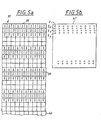
- FIG. 5a shows a particularly advantageous arrangement for a TDI sensor in connection with the present invention.
- d the pixel spacing
- n is the number of part sensors.
- the staggered arrangement of several partial sensors makes it possible, on the one hand, to design the transparent regions imaged on each partial sensor as rectangular partial grids aligned parallel to the rows and columns of the partial sensors.
- the partial grids are offset from one another in accordance with the offset of the partial sensors, so that the entire image field is continuously captured when the image data of the partial TDIs are sorted accordingly in order to obtain the correct order.
- several transparent areas can be mapped onto a column of each partial sensor at different stage positions, which results in an improvement in the signal / noise ratio.
- two transparent areas are depicted on each pixel position at correspondingly offset stage positions of the same part sensor (38).
- the use of only two transparent areas per pixel position is only for illustration.
- the number of transparent areas per pixel position can be selected in accordance with the number of partial sensors (38, 39, 40), which then results in 9 partial sensors results in a light quantity per pixel that is a factor of 9 greater than the exemplary embodiments according to FIGS. 3a-3c and 4a-4c, so that the object can be scanned at 9 times the speed with the same signal / noise ratio.
- a sensor array out several offset sensors can also be arranged in Connection with a normal, non-anamorphic image the aperture array are used on the sensor array; in In this case, however, only a part of the columns of the Partial sensors for image formation.
Landscapes
- Physics & Mathematics (AREA)
- Chemical & Material Sciences (AREA)
- Analytical Chemistry (AREA)
- General Physics & Mathematics (AREA)
- Optics & Photonics (AREA)
- Engineering & Computer Science (AREA)
- Computer Vision & Pattern Recognition (AREA)
- General Engineering & Computer Science (AREA)
- Microscoopes, Condenser (AREA)
- Length Measuring Devices By Optical Means (AREA)
- Testing Or Measuring Of Semiconductors Or The Like (AREA)
Description
- Figur 1a
- die Prinzipskizze eines ersten Ausführungsbeispiels der Erfindung mit einem einzigen, im gemeinsamen Teil des Beleuchtungs- und Beobachtungsstrahlenganges angeordneten Pinholearray;
- Figur 1b
- ein zweites Ausführungsbeispiel der Erfindung mit separatem Lichtquellen- und Blendenarray;
- Figur 1c
- eine Prinzipskizze zur Erläuterung der Synchronisation zwischen Objektbewegung und Ladungsverschiebung im Sensorarray;
- Figur 2a
- ein Blockschaltbild der Synchronisation zwischen Bewegung des Scanntisches und der Ladungsverschiebung im Sensorarray;
- Figur 2b
- eine Detaildarstellung des Funktionsablaufs im Mikrocontroller aus Figur 2a;
- Figuren 3a - 3c
- Ausschnitte aus einem ein rhombisches Gitter bildendes Blendenarray und die zugehörigen Bildpunkte in der Objektebene und in der Ebene des Sensorarrays;
- Figuren 4a - 4c
- Ausschnitte aus einem ein rechtwinkliges Gitter bildendes Blendenarray und der zugehörigen Bildpunkte in der Objektebene und in der Ebene des Sensorarrays;
- Figur 5a
- eine schematische Darstellung eines Sensorarrays aus mehreren versetzt zueinander angeordneten zweidimensionalen Teil-Sensorarrays und
- Figur 5b
- die Prinzipskizze eines für das Sensorarray aus Figur 5a geeigneten Pinholearrays.
Claims (12)
- Konfokales Mikroskop miteinem motorischen Scanningtisch (9) zum Bewegen eines Objektes (8) senkrecht zur optischen Achse des Mikroskopes,einem Blendenarray (4, 4a, 4b) in einer zur Fokusebene des Mikroskopobjektivs (7) konjugierten Ebene,einem dem Blendenarray (4, 4b) nachgeordneten Sensorarray (11) mit einer Vielzahl lichtempfindlicher Elemente, den lichtempfindlichen Elementen zugeordneten Ladungsspeichern und einer Einrichtung zum Verschieben der in den Ladungsspeichern gespeicherten Ladungen von einem Speicher zu einem anderen Speicher, undeiner Synchronisationseinheit (13, 24), die ein Verschieben der Ladungen entsprechend der Bewegung des Bildpunktes eines Objektpunktes in der Ebene des Sensorarrays (11) bewirkt.
- Konfokales Mikroskop nach Anspruch 1, wobei die Bewegung der Probe entlang linearer Bahnen erfolgt.
- Konfokales Mikroskop nach Anspruch 1 oder 2, wobei das Blendenarray (4, 4a, 4b) beim Bewegen der Probe relativ zum Strahlengang fest bleibt.
- Konfokales Mikroskop nach Anspruch 3, wobei das Blendenarray (4, 4b) derart ausgebildet ist, daß die Bahnen der Bilder der transparenten Bereiche (41 - 420) in der Fokusebene des Objektivs (7) einen Teil der Fokusebene lückenlos ausfüllen.
- Konfokales Mikroskop nach einem der Ansprüche 1 - 4, wobei ein Lichtquellenarray (4, 4a) zur Erzeugung einer Vielzahl voneinander beabstandeter Lichtquellen in einer zur Fokusebene des Objektivs (7) konjugierten Ebene angeordnet ist und wobei die Positionen der Lichtquellen zu den Positionen der lichtdurchlässigen Bereiche (41 -420) des Blendenarrays (4, 4b) konjugiert sind.
- Konfokales Mikroskop nach einem der Ansprüche 1 - 5, wobei das Detektorarray (11) eine Vielzahl parallel zueinander angeordneter linearer Sensorspalten aufweist und die Verschiebung der Ladungen in Richtung der Spalten erfolgt.
- Konfokales Mikroskop nach Anspruch 6, wobei das Blendenarray eine Vielzahl lichtdurchlässiger Bereiche (41 - 420) aufweist und wobei auf jede Spalte des Sensorarrays mindestens ein lichtdurchlässiger Bereich (41 - 420) des Blendenarrays (4, 4b) abgebildet ist.
- Konfokales Mikroskop nach Anspruch 7, wobei die lichtdurchlässigen Bereiche des Blendenarrays (4, 4a, 4b) ein zweidimensionales rhombisches Gitter bilden.
- Konfokales Mikroskop nach Anspruch 7, wobei die lichtdurchlässigen Bereiche des Blendenarrays (4, 4a, 4b) ein rechtwinkliges zweidimensionales Gitter bilden.
- Konfokales Mikroskop nach einem der Ansprüche 1-9, wobei das Blendenarray(4, 4b) auf das Sensorarray (11) abgebildet ist.
- Konfokales Mikroskop nach einem der Ansprüche 6 - 10, wobei das Sensorarray (37) mehrere in Spaltenrichtung hintereinander angeordnete, voneinander unabhängige, Teil-Sensorarrays (38, 39, 40) aufweist, die in Zeilenrichtung um einen Betrag zueinander versetzt angeordnet sind, wobei für den Betrag der Versetzung gilt Δ = d / n, und wobei d die Abmessung der Einzelsensoren in Zeilenrichtung und n die Anzahl der Teil-Sensorarrays ist.
- Konfokales Mikroskop nach Anspruch 11, wobei das Blendenarray (41) anamorphotisch auf das Sensorarray (37) abgebildet ist.
Applications Claiming Priority (2)
| Application Number | Priority Date | Filing Date | Title |
|---|---|---|---|
| DE19714221 | 1997-04-07 | ||
| DE19714221A DE19714221A1 (de) | 1997-04-07 | 1997-04-07 | Konfokales Mikroskop mit einem motorischen Scanningtisch |
Publications (2)
| Publication Number | Publication Date |
|---|---|
| EP0871052A1 EP0871052A1 (de) | 1998-10-14 |
| EP0871052B1 true EP0871052B1 (de) | 2004-01-14 |
Family
ID=7825633
Family Applications (1)
| Application Number | Title | Priority Date | Filing Date |
|---|---|---|---|
| EP98105816A Expired - Lifetime EP0871052B1 (de) | 1997-04-07 | 1998-03-31 | Konfokales Mikroskop mit einem motorischen Scanningtisch |
Country Status (4)
| Country | Link |
|---|---|
| US (1) | US6429897B2 (de) |
| EP (1) | EP0871052B1 (de) |
| JP (1) | JP3970998B2 (de) |
| DE (2) | DE19714221A1 (de) |
Cited By (7)
| Publication number | Priority date | Publication date | Assignee | Title |
|---|---|---|---|---|
| US8565480B2 (en) | 2004-05-27 | 2013-10-22 | Leica Biosystems Imaging, Inc. | Creating and viewing three dimensional virtual slides |
| US8755579B2 (en) | 2000-05-03 | 2014-06-17 | Leica Biosystems Imaging, Inc. | Fully automatic rapid microscope slide scanner |
| US8805050B2 (en) | 2000-05-03 | 2014-08-12 | Leica Biosystems Imaging, Inc. | Optimizing virtual slide image quality |
| US8953859B2 (en) | 2005-01-27 | 2015-02-10 | Leica Biosystems Imaging, Inc. | Viewing three dimensional digital slides |
| US9213177B2 (en) | 2000-05-03 | 2015-12-15 | Leica Biosystems Imaging, Inc. | Achieving focus in a digital pathology system |
| US9235041B2 (en) | 2005-07-01 | 2016-01-12 | Leica Biosystems Imaging, Inc. | System and method for single optical axis multi-detector microscope slide scanner |
| US10027855B2 (en) | 2010-06-30 | 2018-07-17 | Ge Healthcare Bio-Science Corp. | System for synchronization in a line scanning imaging microscope |
Families Citing this family (95)
| Publication number | Priority date | Publication date | Assignee | Title |
|---|---|---|---|---|
| JP4042185B2 (ja) * | 1997-08-29 | 2008-02-06 | 株式会社ニコン | パターン検査装置 |
| US6388788B1 (en) | 1998-03-16 | 2002-05-14 | Praelux, Inc. | Method and apparatus for screening chemical compounds |
| US20030036855A1 (en) | 1998-03-16 | 2003-02-20 | Praelux Incorporated, A Corporation Of New Jersey | Method and apparatus for screening chemical compounds |
| US6867406B1 (en) | 1999-03-23 | 2005-03-15 | Kla-Tencor Corporation | Confocal wafer inspection method and apparatus using fly lens arrangement |
| US6847729B1 (en) | 1999-04-21 | 2005-01-25 | Fairfield Imaging Limited | Microscopy |
| DE19921127A1 (de) * | 1999-05-07 | 2000-11-16 | Metasystems Hard & Software Gm | Mikroskopsysteme zur optischen Abtastung von mikroskopischen Objekten sowie Verfahren zur optischen Abtastung |
| JP3544892B2 (ja) | 1999-05-12 | 2004-07-21 | 株式会社東京精密 | 外観検査方法及び装置 |
| DE19956438A1 (de) * | 1999-11-24 | 2001-05-31 | Leica Microsystems | Anordnung zum Scannen einer Objektaufnahmeeinrichtung |
| US7738688B2 (en) | 2000-05-03 | 2010-06-15 | Aperio Technologies, Inc. | System and method for viewing virtual slides |
| DE10024687A1 (de) * | 2000-05-18 | 2001-11-22 | Zeiss Carl Jena Gmbh | Autofokussiereinrichtung für optische Geräte |
| DE10026392A1 (de) * | 2000-05-27 | 2001-11-29 | Leica Microsystems | Verfahren und Anordnung zur Kodierung von Livebildern in der Mikroskopie |
| JP2004505257A (ja) * | 2000-07-27 | 2004-02-19 | ゼテティック・インスティチュート | 共焦点および近接場顕微鏡技術用多重ソースアレイ |
| DE10050529B4 (de) * | 2000-10-11 | 2016-06-09 | Leica Microsystems Cms Gmbh | Verfahren zur Strahlsteuerung in einem Scanmikroskop, Anordnung zur Strahlsteuerung in einem Scanmikroskop und Scanmikroskop |
| WO2002075370A2 (en) * | 2001-03-19 | 2002-09-26 | Weinstein Ronald S | Miniaturized microscope array digital slide scanner |
| US20060023219A1 (en) * | 2001-03-28 | 2006-02-02 | Meyer Michael G | Optical tomography of small objects using parallel ray illumination and post-specimen optical magnification |
| US6944322B2 (en) | 2001-03-28 | 2005-09-13 | Visiongate, Inc. | Optical tomography of small objects using parallel ray illumination and post-specimen optical magnification |
| US6591003B2 (en) * | 2001-03-28 | 2003-07-08 | Visiongate, Inc. | Optical tomography of small moving objects using time delay and integration imaging |
| US7907765B2 (en) * | 2001-03-28 | 2011-03-15 | University Of Washington | Focal plane tracking for optical microtomography |
| GB2373945A (en) * | 2001-03-29 | 2002-10-02 | Isis Innovation | Stereo microscopy |
| DE10122607B4 (de) * | 2001-05-10 | 2006-11-30 | Leica Microsystems Cms Gmbh | Verfahren und Anordnung zur direkten Fourierabbildung von Proben |
| DE10126291C2 (de) | 2001-05-30 | 2003-04-30 | Leica Microsystems | Mikroskop |
| DE10126286A1 (de) * | 2001-05-30 | 2002-12-19 | Leica Microsystems | Verfahren und Vorrichtung zum Punktweisen scannen einer Probe |
| US7009163B2 (en) * | 2001-06-22 | 2006-03-07 | Orbotech Ltd. | High-sensitivity optical scanning using memory integration |
| US6741730B2 (en) | 2001-08-10 | 2004-05-25 | Visiongate, Inc. | Method and apparatus for three-dimensional imaging in the fourier domain |
| AU2002342349A1 (en) | 2001-11-07 | 2003-05-19 | Applied Materials, Inc. | Maskless printer using photoelectric conversion of a light beam array |
| US6946655B2 (en) | 2001-11-07 | 2005-09-20 | Applied Materials, Inc. | Spot grid array electron imaging system |
| US6639201B2 (en) | 2001-11-07 | 2003-10-28 | Applied Materials, Inc. | Spot grid array imaging system |
| JP4097966B2 (ja) * | 2002-03-22 | 2008-06-11 | オリンパス株式会社 | 画像取得装置 |
| US7260253B2 (en) * | 2002-04-19 | 2007-08-21 | Visiongate, Inc. | Method for correction of relative object-detector motion between successive views |
| US7811825B2 (en) * | 2002-04-19 | 2010-10-12 | University Of Washington | System and method for processing specimens and images for optical tomography |
| US20050085708A1 (en) * | 2002-04-19 | 2005-04-21 | University Of Washington | System and method for preparation of cells for 3D image acquisition |
| US7197355B2 (en) | 2002-04-19 | 2007-03-27 | Visiongate, Inc. | Variable-motion optical tomography of small objects |
| US7738945B2 (en) * | 2002-04-19 | 2010-06-15 | University Of Washington | Method and apparatus for pseudo-projection formation for optical tomography |
| US6697508B2 (en) | 2002-05-10 | 2004-02-24 | Visiongate, Inc. | Tomographic reconstruction of small objects using a priori knowledge |
| US6770893B2 (en) * | 2002-05-13 | 2004-08-03 | Visiongate, Inc. | Method and apparatus for emission computed tomography using temporal signatures |
| JP3731073B2 (ja) * | 2002-09-17 | 2006-01-05 | 独立行政法人理化学研究所 | 顕微鏡装置 |
| US7116440B2 (en) | 2003-02-28 | 2006-10-03 | Aperio Technologies, Inc. | Image processing and analysis framework |
| US7257268B2 (en) | 2003-02-28 | 2007-08-14 | Aperio Technologies, Inc. | Systems and methods for image pattern recognition |
| KR100942841B1 (ko) * | 2003-06-02 | 2010-02-18 | 엘지디스플레이 주식회사 | 액정표시소자의 검사 방법 및 장치와 리페어방법 및 장치 |
| US20060018013A1 (en) * | 2004-07-07 | 2006-01-26 | Yoshimasa Suzuki | Microscope imaging apparatus and biological-specimen examination system |
| US6991738B1 (en) | 2004-10-13 | 2006-01-31 | University Of Washington | Flow-through drum centrifuge |
| US20060096358A1 (en) * | 2004-10-28 | 2006-05-11 | University Of Washington | Optical projection tomography microscope |
| US7494809B2 (en) | 2004-11-09 | 2009-02-24 | Visiongate, Inc. | Automated cell sample enrichment preparation method |
| JP5058815B2 (ja) * | 2004-11-24 | 2012-10-24 | バッテル メモリアル インスティチュート | 細胞撮像用の光学システム |
| US7684048B2 (en) | 2005-11-15 | 2010-03-23 | Applied Materials Israel, Ltd. | Scanning microscopy |
| DE102007009550B4 (de) | 2007-02-27 | 2008-12-18 | Ludwig-Maximilian-Universität | Verfahren und Mikroskopvorrichtung zur Beobachtung einer bewegten Probe |
| WO2008137667A1 (en) | 2007-05-04 | 2008-11-13 | Aperio Technologies, Inc. | System and method for quality assurance in pathology |
| EP3543357A1 (de) | 2007-05-08 | 2019-09-25 | Trustees of Boston University | Chemische funktionalisierung von festkörpernanoporen und nanoporenarrays und anwendungen davon |
| US7835561B2 (en) | 2007-05-18 | 2010-11-16 | Visiongate, Inc. | Method for image processing and reconstruction of images for optical tomography |
| JP2010539469A (ja) * | 2007-09-16 | 2010-12-16 | メイア ベン−レヴィ | 周期パターン照明及びtdiによる結像測定システム |
| US7787112B2 (en) * | 2007-10-22 | 2010-08-31 | Visiongate, Inc. | Depth of field extension for optical tomography |
| JP2009181088A (ja) * | 2008-02-01 | 2009-08-13 | Nikon Corp | 共焦点ユニット、共焦点顕微鏡、および共焦点絞り |
| DE102008010435B4 (de) * | 2008-02-21 | 2010-07-29 | Tecan Trading Ag | Datenerfassungsverfahren mit einem Laser Scanner-Gerät |
| US8743195B2 (en) | 2008-10-24 | 2014-06-03 | Leica Biosystems Imaging, Inc. | Whole slide fluorescence scanner |
| US8624971B2 (en) * | 2009-01-23 | 2014-01-07 | Kla-Tencor Corporation | TDI sensor modules with localized driving and signal processing circuitry for high speed inspection |
| US8254023B2 (en) * | 2009-02-23 | 2012-08-28 | Visiongate, Inc. | Optical tomography system with high-speed scanner |
| JP2010216880A (ja) * | 2009-03-13 | 2010-09-30 | Omron Corp | 変位センサ |
| EP2483680A4 (de) | 2009-09-30 | 2014-01-01 | Quantapore Inc | Ultraschnelle sequenzierung biologischer polymere mithilfe einer markierten nanopore |
| US8116547B2 (en) | 2009-12-11 | 2012-02-14 | Aperio Technologies, Inc. | Signal to noise ratio in digital pathology image analysis |
| US8421903B2 (en) * | 2010-05-10 | 2013-04-16 | Abbott Laboratories | Staggered contact image sensor imaging system |
| US8175452B1 (en) * | 2010-10-26 | 2012-05-08 | Complete Genomics, Inc. | Method and system for imaging high density biochemical arrays with sub-pixel alignment |
| DE202011001569U1 (de) * | 2011-01-14 | 2012-03-01 | Berthold Technologies Gmbh & Co. Kg | Vorrichtung zur Messung von optischen Eigenschaften in Mikroplatten |
| US8964088B2 (en) | 2011-09-28 | 2015-02-24 | Semiconductor Components Industries, Llc | Time-delay-and-integrate image sensors having variable intergration times |
| US9971140B2 (en) | 2011-12-19 | 2018-05-15 | Hamamatsu Photonics K.K. | Image capturing apparatus and focusing method thereof |
| DE102012217967A1 (de) | 2012-10-01 | 2014-04-03 | Carl Zeiss Microscopy Gmbh | Konfokales Mikroskop mit frei einstellbarer Probenabtastung |
| US9651539B2 (en) | 2012-10-28 | 2017-05-16 | Quantapore, Inc. | Reducing background fluorescence in MEMS materials by low energy ion beam treatment |
| JP6131448B2 (ja) * | 2012-12-04 | 2017-05-24 | 三星電子株式会社Samsung Electronics Co.,Ltd. | 共焦点光学式検査装置および共焦点光学式検査方法 |
| US20140152797A1 (en) * | 2012-12-04 | 2014-06-05 | Samsung Electronics Co., Ltd. | Confocal optical inspection apparatus and confocal optical inspection method |
| CN105008975B (zh) | 2013-01-17 | 2018-06-26 | 浜松光子学株式会社 | 图像取得装置以及图像取得装置的聚焦方法 |
| HUE054657T2 (hu) * | 2013-01-17 | 2021-09-28 | Hamamatsu Photonics Kk | Képfelvevõ berendezés és fókuszálási eljárás arra |
| EP2947490A4 (de) | 2013-01-17 | 2016-08-31 | Hamamatsu Photonics Kk | Bilderfassungsvorrichtung und verfahren zur fokussierung einer bilderfassungsvorrichtung |
| CN104006949A (zh) * | 2013-02-26 | 2014-08-27 | 北京京东方光电科技有限公司 | 一种透过率检测设备 |
| DE102013005563A1 (de) * | 2013-03-28 | 2014-10-02 | Carl Zeiss Microscopy Gmbh | Lichtmikroskop und verfahren zum untersuchen einer mikroskopischen probe |
| EP3004385B1 (de) | 2013-05-24 | 2018-11-28 | Quantapore Inc. | Nanoporenbasierte nukleinsäureanalyse mit gemischtem fret-nachweis |
| US9772297B2 (en) | 2014-02-12 | 2017-09-26 | Kla-Tencor Corporation | Apparatus and methods for combined brightfield, darkfield, and photothermal inspection |
| FR3018603B1 (fr) * | 2014-03-13 | 2018-03-09 | Holo3 - Association Pour Le Developpement Des Methodes Et Techniques Holographiques Optiques Et Connexes | Dispositif d'analyse et d'imagerie d'une surface par deflectometrie et procede correspondant |
| US9606069B2 (en) * | 2014-06-25 | 2017-03-28 | Kla-Tencor Corporation | Method, apparatus and system for generating multiple spatially separated inspection regions on a substrate |
| ES2789000T3 (es) | 2014-10-10 | 2020-10-23 | Quantapore Inc | Análisis de polinucleótidos basado en nanoporos con marcadores fluorescentes que se inactivan mutuamente |
| US9897791B2 (en) * | 2014-10-16 | 2018-02-20 | Illumina, Inc. | Optical scanning systems for in situ genetic analysis |
| CA2964790C (en) | 2014-10-24 | 2023-02-21 | Quantapore, Inc. | Efficient optical analysis of polymers using arrays of nanostructures |
| US9860466B2 (en) | 2015-05-14 | 2018-01-02 | Kla-Tencor Corporation | Sensor with electrically controllable aperture for inspection and metrology systems |
| US11069054B2 (en) | 2015-12-30 | 2021-07-20 | Visiongate, Inc. | System and method for automated detection and monitoring of dysplasia and administration of immunotherapy and chemotherapy |
| US10313622B2 (en) | 2016-04-06 | 2019-06-04 | Kla-Tencor Corporation | Dual-column-parallel CCD sensor and inspection systems using a sensor |
| US10778925B2 (en) | 2016-04-06 | 2020-09-15 | Kla-Tencor Corporation | Multiple column per channel CCD sensor architecture for inspection and metrology |
| US10823721B2 (en) | 2016-07-05 | 2020-11-03 | Quantapore, Inc. | Optically based nanopore sequencing |
| US10852519B2 (en) * | 2016-11-30 | 2020-12-01 | Asm Technology Singapore Pte Ltd | Confocal imaging of an object utilising a pinhole array |
| JP6863578B2 (ja) * | 2017-04-19 | 2021-04-21 | 日本分光株式会社 | 赤外顕微鏡 |
| US10429315B2 (en) * | 2017-07-18 | 2019-10-01 | Samsung Electronics Co., Ltd. | Imaging apparatus and imaging method |
| JP7115826B2 (ja) * | 2017-07-18 | 2022-08-09 | 三星電子株式会社 | 撮像装置および撮像方法 |
| CN108181005B (zh) * | 2017-11-17 | 2020-09-08 | 天津津航技术物理研究所 | 一种用于tdi ccd探测器焦面调试的方法及系统 |
| WO2021159285A1 (zh) | 2020-02-12 | 2021-08-19 | 深圳华大智造科技股份有限公司 | 光学成像系统及应用所述光学成像系统的生化物质检测系统 |
| CN113479353B (zh) * | 2021-07-14 | 2022-09-06 | 贵州航天林泉电机有限公司 | 一种基于速度规划的卫星转台路径规划方法 |
| DE102022133829A1 (de) | 2022-12-19 | 2024-06-20 | Carl Zeiss Smt Gmbh | Verfahren und Vorrichtung zur Maskeninspektion |
| DE102023202135B9 (de) | 2023-03-09 | 2025-07-24 | Carl Zeiss Smt Gmbh | Sensoranordnung zur Anordnung an einer Messkammer, Vorrichtung zur Qualifizierung einer Maske und Verfahren zur Qualifizierung einer Maske |
| DE102024203350B4 (de) | 2024-04-11 | 2025-12-24 | Carl Zeiss Smt Gmbh | Energie-Detektions-Baugruppe für ein Beleuchtungssystem eines Maskeninspektionssystems zum Einsatz mit EUV-Beleuchtungslicht |
Family Cites Families (9)
| Publication number | Priority date | Publication date | Assignee | Title |
|---|---|---|---|---|
| US4382267A (en) * | 1981-09-24 | 1983-05-03 | Rca Corporation | Digital control of number of effective rows of two-dimensional charge-transfer imager array |
| NL8402340A (nl) * | 1984-07-25 | 1986-02-17 | Philips Nv | Microscoop voor niet-gedifferentieerde fase-beeldvorming. |
| DE69010318T2 (de) * | 1990-01-16 | 1995-01-26 | Philips Nv | Abtastanordnung zum Abtasten einer Oberfläche entlang einer Linie mittels optischer Strahlung. |
| KR960007481B1 (ko) * | 1991-05-27 | 1996-06-03 | 가부시끼가이샤 히다찌세이사꾸쇼 | 패턴검사방법 및 장치 |
| JP2971628B2 (ja) * | 1991-06-27 | 1999-11-08 | 株式会社日立製作所 | パターン検査方法及び装置 |
| JP2954381B2 (ja) * | 1991-05-27 | 1999-09-27 | 株式会社日立製作所 | パターン検査方法及び装置 |
| US5248876A (en) * | 1992-04-21 | 1993-09-28 | International Business Machines Corporation | Tandem linear scanning confocal imaging system with focal volumes at different heights |
| US5544338A (en) * | 1992-12-31 | 1996-08-06 | International Business Machines Corporation | Apparatus and method for raster generation from sparse area array output |
| WO1996039619A1 (en) * | 1995-06-06 | 1996-12-12 | Kla Instruments Corporation | Optical inspection of a specimen using multi-channel responses from the specimen |
-
1997
- 1997-04-07 DE DE19714221A patent/DE19714221A1/de not_active Withdrawn
- 1997-11-18 JP JP31687897A patent/JP3970998B2/ja not_active Expired - Fee Related
-
1998
- 1998-03-31 DE DE59810569T patent/DE59810569D1/de not_active Expired - Lifetime
- 1998-03-31 EP EP98105816A patent/EP0871052B1/de not_active Expired - Lifetime
-
2001
- 2001-02-09 US US09/779,960 patent/US6429897B2/en not_active Expired - Fee Related
Cited By (12)
| Publication number | Priority date | Publication date | Assignee | Title |
|---|---|---|---|---|
| US8755579B2 (en) | 2000-05-03 | 2014-06-17 | Leica Biosystems Imaging, Inc. | Fully automatic rapid microscope slide scanner |
| US8805050B2 (en) | 2000-05-03 | 2014-08-12 | Leica Biosystems Imaging, Inc. | Optimizing virtual slide image quality |
| US9213177B2 (en) | 2000-05-03 | 2015-12-15 | Leica Biosystems Imaging, Inc. | Achieving focus in a digital pathology system |
| US9386211B2 (en) | 2000-05-03 | 2016-07-05 | Leica Biosystems Imaging, Inc. | Fully automatic rapid microscope slide scanner |
| US9535243B2 (en) | 2000-05-03 | 2017-01-03 | Leica Biosystems Imaging, Inc. | Optimizing virtual slide image quality |
| US8565480B2 (en) | 2004-05-27 | 2013-10-22 | Leica Biosystems Imaging, Inc. | Creating and viewing three dimensional virtual slides |
| US8923597B2 (en) | 2004-05-27 | 2014-12-30 | Leica Biosystems Imaging, Inc. | Creating and viewing three dimensional virtual slides |
| US9069179B2 (en) | 2004-05-27 | 2015-06-30 | Leica Biosystems Imaging, Inc. | Creating and viewing three dimensional virtual slides |
| US8953859B2 (en) | 2005-01-27 | 2015-02-10 | Leica Biosystems Imaging, Inc. | Viewing three dimensional digital slides |
| US9349208B2 (en) | 2005-01-27 | 2016-05-24 | Leica Biosystems Imaging, Inc. | Viewing three dimensional digital slides |
| US9235041B2 (en) | 2005-07-01 | 2016-01-12 | Leica Biosystems Imaging, Inc. | System and method for single optical axis multi-detector microscope slide scanner |
| US10027855B2 (en) | 2010-06-30 | 2018-07-17 | Ge Healthcare Bio-Science Corp. | System for synchronization in a line scanning imaging microscope |
Also Published As
| Publication number | Publication date |
|---|---|
| DE19714221A1 (de) | 1998-10-08 |
| US6429897B2 (en) | 2002-08-06 |
| JP3970998B2 (ja) | 2007-09-05 |
| DE59810569D1 (de) | 2004-02-19 |
| EP0871052A1 (de) | 1998-10-14 |
| US20010012069A1 (en) | 2001-08-09 |
| JPH10326587A (ja) | 1998-12-08 |
Similar Documents
| Publication | Publication Date | Title |
|---|---|---|
| EP0871052A1 (de) | Konfokales Mikroskop mit einem motorischen Scanningtisch | |
| DE60001280T2 (de) | Vorrichtung und verfahren zur evaluation eines ziels grosser als die messapertur eines sensors | |
| DE69820856T2 (de) | Interferometersystem und lithographisches gerät mit einem solchen system | |
| DE69418726T2 (de) | Laserabtastmikroskop mit grossem vergrösserungsbereich | |
| DE69511903T2 (de) | System zur kontinnierlichen räumlichen Abbildung für Abtastmikroskopie | |
| DE3854620T2 (de) | Tunnel-abtastmikroskop. | |
| DE69925582T2 (de) | Vorrichtung und verfahren zum optischen messen der oberflächenkontur eines objekts | |
| DE69225915T2 (de) | Abbildungseinrichtung mit einer Vorrichtung zur Detektion eines Fokussierfehlers und/oder einer Verkantung | |
| DE69728572T2 (de) | Mikroabbildungssystem | |
| DE3110287C2 (de) | ||
| DE3337874C2 (de) | ||
| DE102017004428B4 (de) | Verfahren und Anordnung zur robusten, tiefenscannenden fokussierenden Streifen-Triangulation mit mehreren Wavelets | |
| DE102004053730B4 (de) | Verfahren und Anordnung zur Unterdrückung von Falschlicht | |
| DE19626261A1 (de) | Beobachtungsvorrichtung | |
| EP2406679A1 (de) | Autofokusverfahren und autofokuseinrichtung | |
| DE10038622A1 (de) | Scan-Mikroskop,optische Anordnung und Verfahren zur Bildaufnahme in der Scan-Mikroskopie | |
| EP3283917B1 (de) | Verfahren und vorrichtung zum untersuchen einer probe | |
| DE69407078T2 (de) | Bildprojektionsapparat mit Autofokus-System | |
| DE3340647A1 (de) | Verfahren zur fokussierung eines mikroskopes sowie mikroskop zur durchfuehrung des verfahrens | |
| EP4214576B1 (de) | Belichtungssteuerung bei photolithographischen direktbelichtungsverfahren zur leiterplatten- oder schaltkreisherstellung | |
| DE4113279C2 (de) | Konfokales optisches Rastermikroskop | |
| DE102005047200B4 (de) | Verfahren zur Korrektur einer Steuerung eines optischen Scanners in einer Vorrichtung zur scannenden Abbildung einer Probe und Vorrichtung zur Erzeugung eines Bildes einer Probe durch Abscannen der Probe | |
| EP3440492B1 (de) | Verfahren und mikroskop zum untersuchen einer probe | |
| DE102022116214B4 (de) | Messkamera und Verfahren zur zweidimensionalen Vermessung von Gegenständen | |
| DE102017004429B4 (de) | Verfahren und Anordnung zur robusten, tiefenscannenden/fokussierenden Streifen-Triangulation |
Legal Events
| Date | Code | Title | Description |
|---|---|---|---|
| PUAI | Public reference made under article 153(3) epc to a published international application that has entered the european phase |
Free format text: ORIGINAL CODE: 0009012 |
|
| AK | Designated contracting states |
Kind code of ref document: A1 Designated state(s): DE FR GB IT NL |
|
| AX | Request for extension of the european patent |
Free format text: AL;LT;LV;MK;RO;SI |
|
| 17P | Request for examination filed |
Effective date: 19990406 |
|
| AKX | Designation fees paid |
Free format text: DE FR GB IT NL |
|
| GRAP | Despatch of communication of intention to grant a patent |
Free format text: ORIGINAL CODE: EPIDOSNIGR1 |
|
| GRAS | Grant fee paid |
Free format text: ORIGINAL CODE: EPIDOSNIGR3 |
|
| GRAA | (expected) grant |
Free format text: ORIGINAL CODE: 0009210 |
|
| AK | Designated contracting states |
Kind code of ref document: B1 Designated state(s): DE FR GB IT NL |
|
| REG | Reference to a national code |
Ref country code: GB Ref legal event code: FG4D Free format text: NOT ENGLISH |
|
| REF | Corresponds to: |
Ref document number: 59810569 Country of ref document: DE Date of ref document: 20040219 Kind code of ref document: P |
|
| GBT | Gb: translation of ep patent filed (gb section 77(6)(a)/1977) |
Effective date: 20040506 |
|
| RAP2 | Party data changed (patent owner data changed or rights of a patent transferred) |
Owner name: CARL-ZEISS-STIFTUNG TRADING AS CARL ZEISS Owner name: CARL ZEISS |
|
| REG | Reference to a national code |
Ref country code: GB Ref legal event code: 732E |
|
| NLT2 | Nl: modifications (of names), taken from the european patent patent bulletin |
Owner name: CARL ZEISS |
|
| ET | Fr: translation filed | ||
| PLBE | No opposition filed within time limit |
Free format text: ORIGINAL CODE: 0009261 |
|
| STAA | Information on the status of an ep patent application or granted ep patent |
Free format text: STATUS: NO OPPOSITION FILED WITHIN TIME LIMIT |
|
| NLS | Nl: assignments of ep-patents |
Owner name: CARL ZEISS SMT AG |
|
| 26N | No opposition filed |
Effective date: 20041015 |
|
| REG | Reference to a national code |
Ref country code: FR Ref legal event code: TP |
|
| PGFP | Annual fee paid to national office [announced via postgrant information from national office to epo] |
Ref country code: NL Payment date: 20140319 Year of fee payment: 17 Ref country code: DE Payment date: 20140319 Year of fee payment: 17 |
|
| PGFP | Annual fee paid to national office [announced via postgrant information from national office to epo] |
Ref country code: FR Payment date: 20140319 Year of fee payment: 17 Ref country code: IT Payment date: 20140325 Year of fee payment: 17 |
|
| PGFP | Annual fee paid to national office [announced via postgrant information from national office to epo] |
Ref country code: GB Payment date: 20140319 Year of fee payment: 17 |
|
| REG | Reference to a national code |
Ref country code: DE Ref legal event code: R119 Ref document number: 59810569 Country of ref document: DE |
|
| GBPC | Gb: european patent ceased through non-payment of renewal fee |
Effective date: 20150331 |
|
| REG | Reference to a national code |
Ref country code: NL Ref legal event code: MM Effective date: 20150401 |
|
| PG25 | Lapsed in a contracting state [announced via postgrant information from national office to epo] |
Ref country code: IT Free format text: LAPSE BECAUSE OF NON-PAYMENT OF DUE FEES Effective date: 20150331 |
|
| REG | Reference to a national code |
Ref country code: FR Ref legal event code: ST Effective date: 20151130 |
|
| PG25 | Lapsed in a contracting state [announced via postgrant information from national office to epo] |
Ref country code: DE Free format text: LAPSE BECAUSE OF NON-PAYMENT OF DUE FEES Effective date: 20151001 Ref country code: GB Free format text: LAPSE BECAUSE OF NON-PAYMENT OF DUE FEES Effective date: 20150331 |
|
| PG25 | Lapsed in a contracting state [announced via postgrant information from national office to epo] |
Ref country code: FR Free format text: LAPSE BECAUSE OF NON-PAYMENT OF DUE FEES Effective date: 20150331 |
|
| PG25 | Lapsed in a contracting state [announced via postgrant information from national office to epo] |
Ref country code: NL Free format text: LAPSE BECAUSE OF NON-PAYMENT OF DUE FEES Effective date: 20150401 |