EP0843196B1 - Flache Anzeigevorrichtung, ihr Ansteuerverfahren und Verfahren zu ihrer Herstellung - Google Patents
Flache Anzeigevorrichtung, ihr Ansteuerverfahren und Verfahren zu ihrer Herstellung Download PDFInfo
- Publication number
- EP0843196B1 EP0843196B1 EP98100270A EP98100270A EP0843196B1 EP 0843196 B1 EP0843196 B1 EP 0843196B1 EP 98100270 A EP98100270 A EP 98100270A EP 98100270 A EP98100270 A EP 98100270A EP 0843196 B1 EP0843196 B1 EP 0843196B1
- Authority
- EP
- European Patent Office
- Prior art keywords
- signal
- scanning
- display device
- switching
- lines
- Prior art date
- Legal status (The legal status is an assumption and is not a legal conclusion. Google has not performed a legal analysis and makes no representation as to the accuracy of the status listed.)
- Expired - Lifetime
Links
Images


Classifications
-
- G—PHYSICS
- G09—EDUCATION; CRYPTOGRAPHY; DISPLAY; ADVERTISING; SEALS
- G09G—ARRANGEMENTS OR CIRCUITS FOR CONTROL OF INDICATING DEVICES USING STATIC MEANS TO PRESENT VARIABLE INFORMATION
- G09G3/00—Control arrangements or circuits, of interest only in connection with visual indicators other than cathode-ray tubes
- G09G3/20—Control arrangements or circuits, of interest only in connection with visual indicators other than cathode-ray tubes for presentation of an assembly of a number of characters, e.g. a page, by composing the assembly by combination of individual elements arranged in a matrix no fixed position being assigned to or needed to be assigned to the individual characters or partial characters
- G09G3/34—Control arrangements or circuits, of interest only in connection with visual indicators other than cathode-ray tubes for presentation of an assembly of a number of characters, e.g. a page, by composing the assembly by combination of individual elements arranged in a matrix no fixed position being assigned to or needed to be assigned to the individual characters or partial characters by control of light from an independent source
- G09G3/36—Control arrangements or circuits, of interest only in connection with visual indicators other than cathode-ray tubes for presentation of an assembly of a number of characters, e.g. a page, by composing the assembly by combination of individual elements arranged in a matrix no fixed position being assigned to or needed to be assigned to the individual characters or partial characters by control of light from an independent source using liquid crystals
- G09G3/3611—Control of matrices with row and column drivers
- G09G3/3674—Details of drivers for scan electrodes
- G09G3/3677—Details of drivers for scan electrodes suitable for active matrices only
-
- G—PHYSICS
- G02—OPTICS
- G02F—OPTICAL DEVICES OR ARRANGEMENTS FOR THE CONTROL OF LIGHT BY MODIFICATION OF THE OPTICAL PROPERTIES OF THE MEDIA OF THE ELEMENTS INVOLVED THEREIN; NON-LINEAR OPTICS; FREQUENCY-CHANGING OF LIGHT; OPTICAL LOGIC ELEMENTS; OPTICAL ANALOGUE/DIGITAL CONVERTERS
- G02F1/00—Devices or arrangements for the control of the intensity, colour, phase, polarisation or direction of light arriving from an independent light source, e.g. switching, gating or modulating; Non-linear optics
- G02F1/01—Devices or arrangements for the control of the intensity, colour, phase, polarisation or direction of light arriving from an independent light source, e.g. switching, gating or modulating; Non-linear optics for the control of the intensity, phase, polarisation or colour
- G02F1/13—Devices or arrangements for the control of the intensity, colour, phase, polarisation or direction of light arriving from an independent light source, e.g. switching, gating or modulating; Non-linear optics for the control of the intensity, phase, polarisation or colour based on liquid crystals, e.g. single liquid crystal display cells
- G02F1/133—Constructional arrangements; Operation of liquid crystal cells; Circuit arrangements
- G02F1/1333—Constructional arrangements; Manufacturing methods
- G02F1/1345—Conductors connecting electrodes to cell terminals
-
- G—PHYSICS
- G02—OPTICS
- G02F—OPTICAL DEVICES OR ARRANGEMENTS FOR THE CONTROL OF LIGHT BY MODIFICATION OF THE OPTICAL PROPERTIES OF THE MEDIA OF THE ELEMENTS INVOLVED THEREIN; NON-LINEAR OPTICS; FREQUENCY-CHANGING OF LIGHT; OPTICAL LOGIC ELEMENTS; OPTICAL ANALOGUE/DIGITAL CONVERTERS
- G02F1/00—Devices or arrangements for the control of the intensity, colour, phase, polarisation or direction of light arriving from an independent light source, e.g. switching, gating or modulating; Non-linear optics
- G02F1/01—Devices or arrangements for the control of the intensity, colour, phase, polarisation or direction of light arriving from an independent light source, e.g. switching, gating or modulating; Non-linear optics for the control of the intensity, phase, polarisation or colour
- G02F1/13—Devices or arrangements for the control of the intensity, colour, phase, polarisation or direction of light arriving from an independent light source, e.g. switching, gating or modulating; Non-linear optics for the control of the intensity, phase, polarisation or colour based on liquid crystals, e.g. single liquid crystal display cells
- G02F1/133—Constructional arrangements; Operation of liquid crystal cells; Circuit arrangements
- G02F1/136—Liquid crystal cells structurally associated with a semi-conducting layer or substrate, e.g. cells forming part of an integrated circuit
- G02F1/1362—Active matrix addressed cells
-
- G—PHYSICS
- G09—EDUCATION; CRYPTOGRAPHY; DISPLAY; ADVERTISING; SEALS
- G09G—ARRANGEMENTS OR CIRCUITS FOR CONTROL OF INDICATING DEVICES USING STATIC MEANS TO PRESENT VARIABLE INFORMATION
- G09G3/00—Control arrangements or circuits, of interest only in connection with visual indicators other than cathode-ray tubes
- G09G3/20—Control arrangements or circuits, of interest only in connection with visual indicators other than cathode-ray tubes for presentation of an assembly of a number of characters, e.g. a page, by composing the assembly by combination of individual elements arranged in a matrix no fixed position being assigned to or needed to be assigned to the individual characters or partial characters
- G09G3/34—Control arrangements or circuits, of interest only in connection with visual indicators other than cathode-ray tubes for presentation of an assembly of a number of characters, e.g. a page, by composing the assembly by combination of individual elements arranged in a matrix no fixed position being assigned to or needed to be assigned to the individual characters or partial characters by control of light from an independent source
- G09G3/36—Control arrangements or circuits, of interest only in connection with visual indicators other than cathode-ray tubes for presentation of an assembly of a number of characters, e.g. a page, by composing the assembly by combination of individual elements arranged in a matrix no fixed position being assigned to or needed to be assigned to the individual characters or partial characters by control of light from an independent source using liquid crystals
- G09G3/3611—Control of matrices with row and column drivers
- G09G3/3648—Control of matrices with row and column drivers using an active matrix
-
- G—PHYSICS
- G09—EDUCATION; CRYPTOGRAPHY; DISPLAY; ADVERTISING; SEALS
- G09G—ARRANGEMENTS OR CIRCUITS FOR CONTROL OF INDICATING DEVICES USING STATIC MEANS TO PRESENT VARIABLE INFORMATION
- G09G2310/00—Command of the display device
- G09G2310/02—Addressing, scanning or driving the display screen or processing steps related thereto
- G09G2310/0224—Details of interlacing
-
- G—PHYSICS
- G09—EDUCATION; CRYPTOGRAPHY; DISPLAY; ADVERTISING; SEALS
- G09G—ARRANGEMENTS OR CIRCUITS FOR CONTROL OF INDICATING DEVICES USING STATIC MEANS TO PRESENT VARIABLE INFORMATION
- G09G2310/00—Command of the display device
- G09G2310/02—Addressing, scanning or driving the display screen or processing steps related thereto
- G09G2310/0264—Details of driving circuits
- G09G2310/0286—Details of a shift registers arranged for use in a driving circuit
-
- G—PHYSICS
- G09—EDUCATION; CRYPTOGRAPHY; DISPLAY; ADVERTISING; SEALS
- G09G—ARRANGEMENTS OR CIRCUITS FOR CONTROL OF INDICATING DEVICES USING STATIC MEANS TO PRESENT VARIABLE INFORMATION
- G09G2310/00—Command of the display device
- G09G2310/06—Details of flat display driving waveforms
Definitions
- the present invention relates to a flat type display device employing liquid crystals, plasma, a thin film EL (Electro Luminescence), or the like driven through scanning of its display screen, such as a matrix type liquid crystal display device, and relates to a driving method and an assembling method for the display device.
- a flat type display device employing liquid crystals, plasma, a thin film EL (Electro Luminescence), or the like driven through scanning of its display screen, such as a matrix type liquid crystal display device, and relates to a driving method and an assembling method for the display device.
- Fig. 1 shows a conventional thin film transistor (TFT) matrix type liquid crystal display device.
- the liquid crystal display device is constructed by arranging in a matrix form unit cells each composed of a pixel P and a thin film transistor T one terminal of which is connected to the pixel P.
- the gates of the thin film transistors T, T, ... are connected to a scanning conductor line 8 in every row and the other terminals of the above-mentioned thin film transistors T, T, ... are connected to a display conductor line 14 in every column.
- Output signals at scanning signal output terminals 6, 6, ... of scanning drive LSI's (not shown) and output signals at display signal output terminals 12, 12, ... of display drive LSI's (not shown) are supplied to the scanning conductor lines 8, 8, ... and to the display conductor lines 14, 14, ...
- an output signal at one scanning signal output terminal 6 of a scanning signal is supplied to one scanning conductor line 8, as shown in Fig. 1. Therefore, for example, when 240 scanning conductor lines 8 are driven, the scanning drive LSI's are required to produce the same number of output signals, i.e., 240 output signals. In this case, when an LSI which produces 60 output signals is selected, four LSIs are to be provided. When an LSI which produces 80 output signals is selected, three LSIs are to be provided. When an LSI which produces 120 output signals is selected, two LSIs are to be provided.
- Fig. 2 shows another display device wherein ramification conductor lines A, B, C, and D, one end of each ramification conductor line being connected to a scanning signal output terminal 6 and the other end thereof ramifying into n branches, are provided, and a three-terminal transistors SW 11 to SW n4 are provided between the branches and corresponding scanning conductor lines G(1) through G(n) (US-A-4 816 819).
- the corresponding branches of the ramification conductor lines constitute a group, thus n groups of the branches are provided.
- Fig. 3 shows the waveforms of control signals for the display device shown in Fig. 2. In the display device of Fig.
- n control conductor lines E(1) through E(n) connected to the gates of the transistors SW 11 - SW n4 are sequentially selected (electric potential is made to be positive (+V)) to sequentially select the groups of the branches, and the ramification conductor lines A, B, C, and D are sequentially selected when each group of the branches is selected to thereby select the corresponding scanning conductor lines in each group as shown in Fig. 3.
- the scanning conductor lines are selected group by group.
- transistors SW 11 to SW n4 are turned off, transistors P 1 through P N connected to the corresponding scanning conductor lines G(1) through G(N) are turned on (by signals I and J), and a constant voltage is applied to the scanning conductor lines G(1) through G(N) to achieve sufficient discharge of electricity.
- the number of connection terminals of the scanning line drive circuit 5 is smaller than the number of the scanning conductor lines G(1) through G(N).
- the resistance of the conductor lines made of a thin film increases, and therefore the conductor lines may catch noise to cause the malfunction of the display device or the deterioration of the display image quality.
- the scanning line drive circuit 5 and the signal line drive circuit 2 are arranged in two different directions with respect to the display board 1, two connection steps are required for the connection between the display board 1 and the drive circuit boards.
- a junction board 9 for transmitting timing signals and other signals must be provided, and therefore connection between the junction board and the drive circuit boards is required.
- Fig. 4 shows a display device assembling process where the display device shown in Fig. 2 is coupled with a junction board.
- connection material anisotropic conductive film or the like for connecting display conductor lines S(1) through S(M) on the display board (display panel) 1 with the signal line drive circuit 2 is supplied to either the display board 1 or to a signal line drive circuit board (not shown) (step S1).
- the signal line drive circuit board is placed adjacently along a side of the display board 1, that is, the signal line drive circuit board is aligned with the display board 1 (step S2). Then the signal line drive circuit board is connected with the display board so that the display conductor lines S(1) through S(M) on the display board 1 and output terminals of the signal line drive circuit 2 are connected with each other by way of the connection material (step S3). Then the display board 1 is turned by an angle of 90° (step S4).
- the ramification conductor lines A, B, C, and D, the control conductor lines E(1) through E(n), and the other conductor lines on the display board 1 are connected with output terminals of the scanning line drive circuit 5 by means of a connection material (steps S5 - S7). Then the display board 1 with the signal line drive circuit board and the scanning line drive circuit board is transferred (step S8).
- a connection material is supplied to either the junction board or the scanning line drive circuit board (step S9), alignment of both boards is performed (step S10), and conductor lines of the junction board are connected to the input terminals of the scanning line drive circuit 5 (step S11). Then the display board 1 in this condition is transferred (step S12).
- a connection material is supplied to either the junction board or the signal line drive circuit 2 (step S13), alignment of both boards is performed (step S14), and conductor lines of the junction board are connected to the input terminals of the signal line drive circuit 2 (step S15).
- the resulting module disadvantageously has a large size and heavy weight after assembling.
- the display device shown in Fig. 2 has many intersections of the conductor lines, which results in a reduced yield of the products.
- the present invention provides a display device comprising: a substrate; a plurality of scanning conductor lines disposed on the substrate; a plurality of signal conductor lines disposed on the substrate, the signal conductor lines intersecting the scanning conductor lines; a plurality of first switching elements, one first switching element disposed at each intersection between a signal conductor line and a scanning conductor line; a scanning conductor line drive element for driving the scanning conductor lines; a signal conductor line drive element for driving the signal conductor lines; and a plurality of second switching elements, one second switching element disposed between each scanning conductor line and the scanning conductor drive element; characterised in that it further comprises a second switching element drive means for putting the second switching elements into an open state in synchronisation with a fall in the level of a video signal applied to the signal conductor lines thereby to electrically disconnect the scanning conductor lines from the scanning conductor line drive element.
- the second switching element drive means comprises an interruption signal terminal electrically connected to all the second switching elements; and means for applying an interruption control signal to the interruption signal terminal in synchronisation with a fall in the level of the video signal applied to the signal conductor lines.
- the display device further comprises an external power input terminal connected, in use, to an external power source having an OFF voltage sufficient to turn off the first switching elements; a plurality of third switching elements, one third switching element associated with each scanning conductor line for selectively connecting the scanning conductor line to the external power input terminal; and third switching element drive means for applying a switching control signal to the third switching elements when the second switching elements are in an open state, so that when the second switching elements are in an open state the OFF voltage is supplied to the associated scanning conductor line so as sufficiently to turn off the first switching elements associated with the scanning conductor line.
- the third switching element drive means comprises an input terminal connected to all the third switching elements, and means for applying the switching control signal to the input terminal.
- a display device further comprising an external power input terminal connected to an external power source having an OFF voltage sufficient to turn off the first switches, and a third switching element provided on each scanning conductor line for switching a signal to be transmitted through each scanning conductor line between a scanning signal supplied from the scanning conductor line drive element and the OFF voltage, wherein the second switching element is in an open state, a switching control signal is given to an input terminal of the third switching element so that the OFF voltage is supplied to the scanning conductor line to sufficiently turn off the first switching element.
- the first switching element is sufficiently turned off to easily solve the above-mentioned problem.
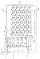
- Fig. 5 shows an active-matrix display device in accordance with an embodiment of the present invention.
- a transparent insulating board 302 which is made of glass and which has a laterally elongated rectangular shape are provided a plurality of gate lines 307 serving as scanning conductor lines and a plurality of source lines 308 serving as signal lines perpendicularly intersecting the gate lines 307.
- the gate lines 307 are arranged in the horizontal direction, while the source lines 308 are arranged in the vertical direction.
- pixels 303 In the areas surrounded by the gate lines 307 and the source lines 308 are provided pixels 303 in a matrix form. At the intersections between the gate lines 307 and the source lines 308 are provided thin film transistors 304 serving as switching elements. At a lengthwise end portion of the transparent insulating board 302 is provided a gate line drive element 305 extending in the widthwise direction, where the gate line drive element 305 is connected to an end of each of the gate lines 307. At a widthwise end portion of the transparent insulating board 302 is provided a source line drive element 306 extending in the lengthwise direction, where the source line drive element 306 is connected to an end of each of the source lines 308.
- the gate line drive element 305 and the source line drive element 306 are practically provided on the transparent insulating board pattern by the COG (Chip On Glass) connection method.
- the gate line drive element 305 is connected to a plurality of input terminal lines 310.
- the gate line drive element 305 sequentially scans the gate lines 307 in the vertical direction while the source line drive element 306 applies a video signal to a source line 308 to write the signal line by line to thereby make the active-matrix display device perform an image display operation.
- Portions of the transparent insulating board 302 except for the portions where the gate line drive element 305 and the source line drive element 306 are provided serve as a display section 301.
- interruption thin film transistors 309 serving as switching elements to make and break a connection between them.
- the gate electrodes of the interruption thin film transistors 309 are connected to an interruption signal input terminal 316 formed on the transparent insulating board 302 in a position slightly apart toward an end of the board 302 from the aforementioned input terminal lines 310, and an interruption control signal 313 is input from an external control circuit (not shown) via the interruption signal input terminal 316.
- FIG. 6 shows the waveforms of a video signal 311 supplied to the source lines 308, a scanning signal 312 given to the gate lines 307, and an interruption control signal 313 input to the interruption signal input terminal 316 for the interruption thin film transistor 309, respectively.
- Fig. 6 (d) shows the waveform of a certain signal inside the gate line drive element 305.
- the interruption thin film transistor 309 is provided to prevent the possible bad influence of an instantaneous voltage drop 315 attributed to the change in level from "H" to "L” of the video signal 311 supplied to the source lines 308 from being exerted on the gate line drive element 305.
- the interruption control signal 313 having the waveform shown in (c) is given to the interruption signal input terminal 316 for the interruption thin film transistors 309 temporarily in synchronization with the fall from "H" to "L” of the video signal 311 in the present embodiment. While the control signal 313 is given, the interruption thin film transistors 309 are off to open the connection between the gate lines 307 and the gate line drive element 305, i.e., temporarily electrically disconnect the gate lines 307 from the gate line drive element 305.
- the interruption thin film transistor 309 is on to connect the gate line drive element 305 with the gate lines 307.
- the instantaneous voltage drop 315 at the gate lines will be transmitted to the gate line drive element 305 and affect various signals (represented by the signal 314) therein so that a momentary change of voltage takes place to the signal 314 as shown in Fig. 9.
- the gate line drive element 305 neither malfunctions nor is subjected to total breakdown due to a voltage exceeding its endurance voltage. Furthermore, since no momentary change of voltage due to the instantaneous voltage drop takes place, a great voltage difference between the "on" voltage and the "off" voltage for the thin film transistor 304 is ensured within the range of the endurance voltage of the gate line drive element 305. The voltage difference is sufficient to easily improve the display quality.
- an active-matrix display device having the gate lines always electrically connected with the gate line drive element is formed by the COG connection method, a resistance combined with the connection resistance and the resistance of the patterned conductor lines on the display board will be exerted on the input terminal lines 310 of the gate line drive element 305 and enlarge the momentary change of voltage due to the instantaneous voltage drop 315.
- the gate lines 307 are designed to be electrically disconnected from the gate line drive element 305 when the instantaneous voltage drop 315 occurs, the instantaneous voltage drop 315 is not transmitted to the gate line drive element 305 and the voltage change of the signal 314 in the gate line drive element 305 as shown in Fig. 9 is avoided.
- Fig. 7 shows an active-matrix display device in accordance with another embodiment of the present invention.
- the present embodiment takes the measure of avoiding the condition where the thin film transistors 304 are not sufficiently turned off due to the possible instability of the electric potential at the gate lines 307 when the gate lines 307 are electrically disconnected from the gate line drive element 305 by the operation of the interruption thin film transistors 309.
- the following describes the detail of the construction. It should be noted that the construction of most of the parts is similar to that in Fig. 5, and therefore like components are denoted by the same reference numerals in Figs. 5 and 7 and no further description on those components is provided here.
- each gate line signal switching thin film transistor 317 is connected to a control signal input terminal 319 provided at a portion adjacent to the interruption signal input terminal 316 on the transparent insulating board 302, and a power switching control signal 320 (see Fig. 8 (e)) is input via the control signal input terminal 319 from an external circuit.
- each switching thin film transistor 317 is connected to the thin film transistor 304, while the drain electrode thereof is connected to an external power input terminal 318.
- the external power input terminal 318 is formed in a position slightly apart from the input terminal line 310 at the opposite side from the interruption signal input terminal 316 and control signal input terminal 319, and an OFF voltage signal 321 is input via the external power input terminal 318 from an external power source.
- the signal 320 is given to the gate electrode of the switching thin film transistor 317 at the time as shown in Fig. 8, i.e., when the video signal 311 falls from "H” to "L” and an interruption control signal 314 at an OFF level is input to the interruption thin film transistors 309.
- an OFF voltage 321 is given to the thin film transistors 304 via the external power input terminal 318 and the switching thin film transistors 317.
- an OFF voltage to sufficiently turn transistors off is supplied to the thin film transistors 304 when the gate lines 307 are made to be electrically disconnected from the gate line drive element 305 by the operation of the interruption thin film transistors 309. Therefore, the insufficient turning off of the thin film transistors 304 due to the unstable electric potential at the gate lines 307 can be securely prevented.
- the present invention can be also applied to the case where a TAB (Tape Automated Bonding) drive element is formed by the COF (Chip On Film) method or to the case where a drive element is formed on a glass board.
- TAB Pear Automated Bonding
- COF Chip On Film
- the thin film transistor to be used in the present invention is typically an insulated gate field effect transistor using amorphous silicon, polysilicon, Te, or the like as a semiconductor material.
- the active-matrix display device of the present invention can be applied not only to a monochrome liquid crystal display device but also to a color liquid crystal display device employing a color filter.
- the various signals inside the scanning conductor line drive element can be kept stable, and therefore the possible malfunction or breakdown of the element due to a voltage exceeding the endurance voltage of the scanning conductor line drive element can be securely prevented. Furthermore, the momentary change of voltage attributed to the instantaneous voltage drop does not takes place, and therefore a great voltage difference can be assured between the "on" voltage and the "off" voltage of the first switching element within the range of the endurance voltage of the gate line drive element.
- the present invention can provide a high-quality, high-reliability active-matrix display device.
- the active-matrix display device shown in Fig. 8 can further improve the reliability, because the first switching elements 304 are prevented from being insufficiently turned off due to the instability of the electric potential at the gate lines while the connection between the scanning conductor lines and the scanning conductor line drive element is undone.
Claims (4)
- Anzeigevorrichtung mit: einem Substrat (302); einer Vielzahl von Abrasterleiterbahnen (307), die auf dem Substrat angeordnet sind; einer Vielzahl von Signalleiterbahnen (308), die auf dem Substrat angeordnet sind und die Abrasterleiterbahnen schneiden; einer Vielzahl erster Schaltelemente (304), von denen ein erstes an jeder Schnittstelle zwischen einer Signalleiterbahn und einer Abrasterleiterbahn angeordnet ist; einem Abrasterleiterbahn-Ansteuerungselement (305) zum Ansteuern der Abrasterleiterbahnen; einem Signalleiterbahn-Ansteuerungselement (306) zum Ansteuern der Signalleiterbahnen; und einer Vielzahl zweiter Schaltelemente (309), wobei ein zweites Schaltelement zwischen jeder Abrasterleiterbahn und dem Abrasterleiterbahn-Ansteuerungselement angeordnet ist; dadurch gekennzeichnet, dass sie ferner eine zweite Schaltelement-Ansteuerungseinrichtung (316) zum Versetzen der zweiten Schaltelemente in einen offenen Zustand synchron mit einem Pegelabfall eines an die Signalleiterbahnen gelegten Videosignals (311) in einen offenen Zustand, um dadurch die Abrasterleiterbahnen (307) elektrisch vom Abrasterleiterbahn-Ansteuerungselement (305) zu trennen, aufweist.
- Anzeigevorrichtung nach Anspruch 1, bei der die zweite Schaltelement-Ansteuerungseinrichtung einen Unterbrechungssignalanschluss (316), der mit allen zweiten Schaltelementen verbunden ist, und eine Einrichtung zum Anlegen eines Unterbrechungssteuerungssignals (313) an den Unterbrechungssignalanschluss (316) synchron mit einem Pegelabfall des an die Signalleiterbahn gelegten Videosignals (311) aufweist.
- Anzeigevorrichtung nach Anspruch 1 oder 2, und ferner mit einem Externspannungs-Eingangsanschluss (318), der im Gebrauch mit einer externen Spannungsquelle mit einer zum Ausschalten der ersten Schaltelemente (304) ausreichenden AUS-Spannung verbunden ist; einer Vielzahl dritter Schaltelemente (317), von denen eines jeder Abrasterleiterbahn zugeordnet ist, um dieselbe selektiv mit dem Externspannungs-Eingangsanschluss zu verbinden; und einer dritten Schaltelement-Ansteuerungseinrichtung (319) zum Anlegen eines Umschaltsteuerungssignals (320) an die dritten Schaltelemente (317), wenn sich die zweiten Schaltelemente in einem offenen Zustand befinden, so dass dann, wenn sich die zweiten Schaltelemente in einem offenen Zustand befinden, die AUS-Spannung an die zugehörige Abrasterleiterbahn gelegt wird, um die der Abrasterleiterbahn zugeordneten ersten Schaltelemente ausreichend auszuschalten.
- Anzeigevorrichtung nach Anspruch 3, bei der die dritte Schaltelement-Ansteuerungseinrichtung einen mit allen dritten Schaltelementen (317) verbundenen Eingangsanschluss (319) und eine Einrichtung zum Anlegen des Umschaltsteuerungssignals (320) an den Eingangsanschluss aufweist.
Applications Claiming Priority (13)
| Application Number | Priority Date | Filing Date | Title |
|---|---|---|---|
| JP330718/92 | 1992-12-10 | ||
| JP33071892 | 1992-12-10 | ||
| JP33071892A JPH06175103A (ja) | 1992-12-10 | 1992-12-10 | アクティブマトリクス表示装置 |
| JP78/93 | 1993-01-04 | ||
| JP7893 | 1993-01-04 | ||
| JP7893 | 1993-01-04 | ||
| JP5213853A JP3053722B2 (ja) | 1993-01-04 | 1993-08-30 | 表示装置の実装構造およびフレキシブル基板の製造方法 |
| JP21385393 | 1993-08-30 | ||
| JP213853/93 | 1993-08-30 | ||
| JP28129693 | 1993-11-10 | ||
| JP5281296A JP3071622B2 (ja) | 1993-11-10 | 1993-11-10 | 表示装置およびその駆動方法およびその実装方法 |
| JP281296/93 | 1993-11-10 | ||
| EP93309942A EP0601869B1 (de) | 1992-12-10 | 1993-12-10 | Flache Anzeigevorrichtung und Verfahren zu ihrer Herstellung |
Related Parent Applications (1)
| Application Number | Title | Priority Date | Filing Date |
|---|---|---|---|
| EP93309942A Division EP0601869B1 (de) | 1992-12-10 | 1993-12-10 | Flache Anzeigevorrichtung und Verfahren zu ihrer Herstellung |
Publications (2)
| Publication Number | Publication Date |
|---|---|
| EP0843196A1 EP0843196A1 (de) | 1998-05-20 |
| EP0843196B1 true EP0843196B1 (de) | 2001-03-28 |
Family
ID=27453088
Family Applications (3)
| Application Number | Title | Priority Date | Filing Date |
|---|---|---|---|
| EP98123224A Expired - Lifetime EP0909975B1 (de) | 1992-12-10 | 1993-12-10 | Flache Anzeigevorrichtung, ihr Ansteuerungsverfahren und Verfahren zu ihrer Herstellung |
| EP98100270A Expired - Lifetime EP0843196B1 (de) | 1992-12-10 | 1993-12-10 | Flache Anzeigevorrichtung, ihr Ansteuerverfahren und Verfahren zu ihrer Herstellung |
| EP93309942A Expired - Lifetime EP0601869B1 (de) | 1992-12-10 | 1993-12-10 | Flache Anzeigevorrichtung und Verfahren zu ihrer Herstellung |
Family Applications Before (1)
| Application Number | Title | Priority Date | Filing Date |
|---|---|---|---|
| EP98123224A Expired - Lifetime EP0909975B1 (de) | 1992-12-10 | 1993-12-10 | Flache Anzeigevorrichtung, ihr Ansteuerungsverfahren und Verfahren zu ihrer Herstellung |
Family Applications After (1)
| Application Number | Title | Priority Date | Filing Date |
|---|---|---|---|
| EP93309942A Expired - Lifetime EP0601869B1 (de) | 1992-12-10 | 1993-12-10 | Flache Anzeigevorrichtung und Verfahren zu ihrer Herstellung |
Country Status (3)
| Country | Link |
|---|---|
| US (1) | US5585815A (de) |
| EP (3) | EP0909975B1 (de) |
| DE (3) | DE69332935T2 (de) |
Families Citing this family (28)
| Publication number | Priority date | Publication date | Assignee | Title |
|---|---|---|---|---|
| US6747627B1 (en) | 1994-04-22 | 2004-06-08 | Semiconductor Energy Laboratory Co., Ltd. | Redundancy shift register circuit for driver circuit in active matrix type liquid crystal display device |
| US6169530B1 (en) * | 1995-04-20 | 2001-01-02 | Canon Kabushiki Kaisha | Display apparatus and assembly of its driving circuit |
| US6683594B1 (en) | 1995-04-20 | 2004-01-27 | Canon Kabushiki Kaisha | Display apparatus and assembly of its driving circuit |
| KR100235589B1 (ko) * | 1997-01-08 | 1999-12-15 | 구본준 | 박막트랜지스터 액정표시장치의 구동방법 |
| KR100235590B1 (ko) * | 1997-01-08 | 1999-12-15 | 구본준 | 박막트랜지스터 액정표시장치의 구동방법 |
| KR100218375B1 (ko) * | 1997-05-31 | 1999-09-01 | 구본준 | 전하 재활용을 이용한 티에프티-엘씨디의 저전력 게이트드라이버회로 |
| US7304632B2 (en) * | 1997-05-13 | 2007-12-04 | Oki Electric Industry Co., Ltd. | Liquid-crystal display driving circuit and method |
| JPH1130975A (ja) * | 1997-05-13 | 1999-02-02 | Oki Electric Ind Co Ltd | 液晶表示装置の駆動回路及びその駆動方法 |
| US6262702B1 (en) * | 1997-10-31 | 2001-07-17 | Seiko Epson Corporation | Electro-optical device and electronic apparatus |
| US6965361B1 (en) * | 1998-06-16 | 2005-11-15 | Agilent Technologies, Inc. | Method of manufacture of active matrix addressed polymer LED display |
| TW580672B (en) * | 1999-03-15 | 2004-03-21 | Seiko Epson Corp | Liquid-crystal display device and method of driving the same |
| JP4926329B2 (ja) * | 2001-03-27 | 2012-05-09 | 株式会社半導体エネルギー研究所 | 半導体装置およびその作製方法、電気器具 |
| TW511047B (en) * | 2001-06-12 | 2002-11-21 | Prime View Int Co Ltd | Scan driving circuit and method for an active matrix liquid crystal display |
| JP2004163493A (ja) * | 2002-11-11 | 2004-06-10 | Sanyo Electric Co Ltd | 表示装置 |
| JP2006098880A (ja) * | 2004-09-30 | 2006-04-13 | Sanyo Electric Co Ltd | 液晶表示装置 |
| KR20060090076A (ko) * | 2005-02-07 | 2006-08-10 | 삼성전자주식회사 | 표시 장치와 이의 구동 방법 |
| JP2007179017A (ja) * | 2005-12-01 | 2007-07-12 | Seiko Instruments Inc | 画像表示装置、及び画像表示方法 |
| WO2007118332A1 (en) * | 2006-04-19 | 2007-10-25 | Ignis Innovation Inc. | Stable driving scheme for active matrix displays |
| JP2008116917A (ja) * | 2006-10-10 | 2008-05-22 | Seiko Epson Corp | ゲートドライバ、電気光学装置、電子機器及び駆動方法 |
| JP4775408B2 (ja) * | 2008-06-03 | 2011-09-21 | ソニー株式会社 | 表示装置、表示装置における配線のレイアウト方法および電子機器 |
| CN101719352B (zh) * | 2008-10-09 | 2012-07-25 | 北京京东方光电科技有限公司 | 液晶盒成盒后检测装置和方法 |
| US8823625B2 (en) * | 2010-10-18 | 2014-09-02 | Shenzhen China Star Optoelectronics Technology Co. Ltd. | LCD device capable of changing the scan order and driving method thereof |
| CN101996603B (zh) | 2010-10-18 | 2012-09-12 | 深圳市华星光电技术有限公司 | 液晶显示装置及其驱动方法 |
| CN103680437A (zh) * | 2013-11-11 | 2014-03-26 | 京东方科技集团股份有限公司 | 电流获取装置、驱动装置及方法、阵列基板及其制备方法 |
| WO2017038849A1 (ja) * | 2015-09-04 | 2017-03-09 | 国立研究開発法人科学技術振興機構 | コネクタ基板、センサーシステム及びウェアラブルなセンサーシステム |
| CN108665860B (zh) | 2017-03-30 | 2019-11-08 | 京东方科技集团股份有限公司 | 一种goa单元及其驱动方法、goa驱动电路、显示装置 |
| KR20200110489A (ko) * | 2019-03-13 | 2020-09-24 | 삼성디스플레이 주식회사 | 플렉시블 표시 장치와 그를 포함한 증강 현실 제공 장치 |
| JP7217650B2 (ja) * | 2019-03-18 | 2023-02-03 | 株式会社ジャパンディスプレイ | 表示装置 |
Citations (1)
| Publication number | Priority date | Publication date | Assignee | Title |
|---|---|---|---|---|
| US4816819A (en) * | 1984-11-26 | 1989-03-28 | Canon Kabushiki Kaisha | Display panel |
Family Cites Families (13)
| Publication number | Priority date | Publication date | Assignee | Title |
|---|---|---|---|---|
| JPS58137892A (ja) * | 1982-02-10 | 1983-08-16 | 株式会社東芝 | ディスプレイ装置 |
| JPH0668672B2 (ja) * | 1984-09-12 | 1994-08-31 | ソニー株式会社 | 液晶デイスプレイ装置 |
| JPS6180226A (ja) * | 1984-09-28 | 1986-04-23 | Toshiba Corp | アクテイブ・マトリツクス駆動装置 |
| GB2166899B (en) * | 1984-11-09 | 1987-12-16 | Hitachi Ltd | Liquid crystal display device |
| KR900009055B1 (ko) * | 1986-05-13 | 1990-12-17 | 상요덴기 가부시기가이샤 | 영상 표시 장치용 구동 회로 |
| JPS6388525A (ja) * | 1986-10-01 | 1988-04-19 | Hitachi Ltd | 走査回路 |
| JP2581796B2 (ja) * | 1988-04-25 | 1997-02-12 | 株式会社日立製作所 | 表示装置及び液晶表示装置 |
| DE69013239T2 (de) * | 1989-06-20 | 1995-05-04 | Sharp Kk | Matrixanzeigevorrichtung. |
| US5105288A (en) * | 1989-10-18 | 1992-04-14 | Matsushita Electronics Corporation | Liquid crystal display apparatus with the application of black level signal for suppressing light leakage |
| JP2969220B2 (ja) * | 1990-05-25 | 1999-11-02 | 京セラ株式会社 | 酸化物超電導体の製造方法 |
| JP3013433B2 (ja) * | 1990-11-08 | 2000-02-28 | セイコーエプソン株式会社 | 配線接続構造および電気光学装置 |
| JP2825985B2 (ja) * | 1991-02-21 | 1998-11-18 | アルプス電気株式会社 | Lcdモジュールの配線構造 |
| JP2587546B2 (ja) * | 1991-03-22 | 1997-03-05 | 株式会社ジーティシー | 走査回路 |
-
1993
- 1993-12-10 DE DE69332935T patent/DE69332935T2/de not_active Expired - Lifetime
- 1993-12-10 EP EP98123224A patent/EP0909975B1/de not_active Expired - Lifetime
- 1993-12-10 DE DE69330074T patent/DE69330074T2/de not_active Expired - Lifetime
- 1993-12-10 EP EP98100270A patent/EP0843196B1/de not_active Expired - Lifetime
- 1993-12-10 EP EP93309942A patent/EP0601869B1/de not_active Expired - Lifetime
- 1993-12-10 DE DE69326419T patent/DE69326419T2/de not_active Expired - Lifetime
-
1995
- 1995-05-10 US US08/437,977 patent/US5585815A/en not_active Expired - Lifetime
Patent Citations (1)
| Publication number | Priority date | Publication date | Assignee | Title |
|---|---|---|---|---|
| US4816819A (en) * | 1984-11-26 | 1989-03-28 | Canon Kabushiki Kaisha | Display panel |
Also Published As
| Publication number | Publication date |
|---|---|
| EP0909975A2 (de) | 1999-04-21 |
| DE69332935D1 (de) | 2003-06-05 |
| DE69330074T2 (de) | 2001-09-06 |
| DE69326419D1 (de) | 1999-10-21 |
| EP0601869B1 (de) | 1999-09-15 |
| DE69326419T2 (de) | 2000-02-17 |
| EP0843196A1 (de) | 1998-05-20 |
| EP0601869A2 (de) | 1994-06-15 |
| EP0601869A3 (de) | 1995-05-10 |
| EP0909975A3 (de) | 1999-05-06 |
| DE69330074D1 (de) | 2001-05-03 |
| DE69332935T2 (de) | 2004-02-26 |
| EP0909975B1 (de) | 2003-05-02 |
| US5585815A (en) | 1996-12-17 |
Similar Documents
| Publication | Publication Date | Title |
|---|---|---|
| EP0843196B1 (de) | Flache Anzeigevorrichtung, ihr Ansteuerverfahren und Verfahren zu ihrer Herstellung | |
| US7522145B2 (en) | Liquid crystal display apparatus | |
| US5657139A (en) | Array substrate for a flat-display device including surge protection circuits and short circuit line or lines | |
| US5828429A (en) | Electro-optical device and method of driving with voltage supply lines parallel to gate lines and two transistors per pixel | |
| US7733312B2 (en) | Liquid crystal display with a structure for reducing corrosion of display signal lines | |
| US7071928B2 (en) | Liquid crystal display device having quad type color filters | |
| KR0175723B1 (ko) | 액티브 매트릭스 표시장치 | |
| CN101093846A (zh) | 布线结构和显示装置 | |
| JP2002006331A (ja) | 液晶表示装置 | |
| EP1049956B1 (de) | Aktivmatrix-flüssigkristall-anzeigevorrichtungen | |
| KR100286489B1 (ko) | 액티브 매트릭스형 표시장치 | |
| JPH07311392A (ja) | 液晶表示装置 | |
| US20020105508A1 (en) | Display device | |
| KR100392603B1 (ko) | 액정표시장치용 구동 아이씨 연결부 | |
| US6603455B1 (en) | Display panel drive circuit and display panel | |
| KR100990315B1 (ko) | 액정표시장치 | |
| JP3272296B2 (ja) | 液晶表示装置 | |
| KR101021747B1 (ko) | 액정표시장치 | |
| KR20050086901A (ko) | 능동 매트릭스 디스플레이 장치 | |
| KR20040055188A (ko) | 박막트랜지스터 기판과 이를 이용한 액정표시장치 | |
| JP3311835B2 (ja) | 表示装置用駆動回路およびそれを用いた液晶表示装置 | |
| KR100534377B1 (ko) | 액정 표시 장치 및 그 제조 방법 | |
| KR100859472B1 (ko) | 액정 표시장치 | |
| KR19990024712A (ko) | 액정표시장치 하판 글래스의 배선구조 | |
| JPH0316028B2 (de) |
Legal Events
| Date | Code | Title | Description |
|---|---|---|---|
| PUAI | Public reference made under article 153(3) epc to a published international application that has entered the european phase |
Free format text: ORIGINAL CODE: 0009012 |
|
| 17P | Request for examination filed |
Effective date: 19980129 |
|
| AC | Divisional application: reference to earlier application |
Ref document number: 601869 Country of ref document: EP |
|
| AK | Designated contracting states |
Kind code of ref document: A1 Designated state(s): DE GB |
|
| RIN1 | Information on inventor provided before grant (corrected) |
Inventor name: YAMAMOTO, YUJI Inventor name: AKIYAMA, HIDEMI Inventor name: SHIMOKAWA, HIROSHI Inventor name: TAGUSA, YASUNOBU Inventor name: INADA, KIYOSHI Inventor name: NAKASHIMA, TAKASHI |
|
| 17Q | First examination report despatched |
Effective date: 19990322 |
|
| GRAG | Despatch of communication of intention to grant |
Free format text: ORIGINAL CODE: EPIDOS AGRA |
|
| GRAG | Despatch of communication of intention to grant |
Free format text: ORIGINAL CODE: EPIDOS AGRA |
|
| GRAG | Despatch of communication of intention to grant |
Free format text: ORIGINAL CODE: EPIDOS AGRA |
|
| GRAH | Despatch of communication of intention to grant a patent |
Free format text: ORIGINAL CODE: EPIDOS IGRA |
|
| GRAH | Despatch of communication of intention to grant a patent |
Free format text: ORIGINAL CODE: EPIDOS IGRA |
|
| GRAA | (expected) grant |
Free format text: ORIGINAL CODE: 0009210 |
|
| AC | Divisional application: reference to earlier application |
Ref document number: 601869 Country of ref document: EP |
|
| AK | Designated contracting states |
Kind code of ref document: B1 Designated state(s): DE GB |
|
| REF | Corresponds to: |
Ref document number: 69330074 Country of ref document: DE Date of ref document: 20010503 |
|
| EN | Fr: translation not filed | ||
| REG | Reference to a national code |
Ref country code: GB Ref legal event code: IF02 |
|
| PLBE | No opposition filed within time limit |
Free format text: ORIGINAL CODE: 0009261 |
|
| STAA | Information on the status of an ep patent application or granted ep patent |
Free format text: STATUS: NO OPPOSITION FILED WITHIN TIME LIMIT |
|
| 26N | No opposition filed | ||
| PGFP | Annual fee paid to national office [announced via postgrant information from national office to epo] |
Ref country code: DE Payment date: 20121205 Year of fee payment: 20 |
|
| PGFP | Annual fee paid to national office [announced via postgrant information from national office to epo] |
Ref country code: GB Payment date: 20121205 Year of fee payment: 20 |
|
| REG | Reference to a national code |
Ref country code: DE Ref legal event code: R071 Ref document number: 69330074 Country of ref document: DE |
|
| REG | Reference to a national code |
Ref country code: GB Ref legal event code: PE20 Expiry date: 20131209 |
|
| PG25 | Lapsed in a contracting state [announced via postgrant information from national office to epo] |
Ref country code: DE Free format text: LAPSE BECAUSE OF EXPIRATION OF PROTECTION Effective date: 20131211 Ref country code: GB Free format text: LAPSE BECAUSE OF EXPIRATION OF PROTECTION Effective date: 20131209 |