EP0833451A2 - Circuit comportant des blocs combinatoires avec registres intermédiaires - Google Patents
Circuit comportant des blocs combinatoires avec registres intermédiaires Download PDFInfo
- Publication number
- EP0833451A2 EP0833451A2 EP97115362A EP97115362A EP0833451A2 EP 0833451 A2 EP0833451 A2 EP 0833451A2 EP 97115362 A EP97115362 A EP 97115362A EP 97115362 A EP97115362 A EP 97115362A EP 0833451 A2 EP0833451 A2 EP 0833451A2
- Authority
- EP
- European Patent Office
- Prior art keywords
- output
- input
- register
- kbl
- circuit
- Prior art date
- Legal status (The legal status is an assumption and is not a legal conclusion. Google has not performed a legal analysis and makes no representation as to the accuracy of the status listed.)
- Granted
Links
Images


Classifications
-
- H—ELECTRICITY
- H03—ELECTRONIC CIRCUITRY
- H03K—PULSE TECHNIQUE
- H03K19/00—Logic circuits, i.e. having at least two inputs acting on one output; Inverting circuits
- H03K19/01—Modifications for accelerating switching
- H03K19/017—Modifications for accelerating switching in field-effect transistor circuits
- H03K19/01728—Modifications for accelerating switching in field-effect transistor circuits in synchronous circuits, i.e. by using clock signals
Definitions
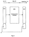
- the runtime of a combinatorial circuit KBL is in this regard designed that always the last possible signal value changes determine the runtime at their outputs. Here it is assumed that these cases are always in operation enter.
- the object of the invention is to take advantage of the above-mentioned effect and to tap values at the output of a combinatorial circuit depending on the event. This object is achieved according to the features of patent claim 1.
- registers will always be a clocked memory element referred to, regardless of whether it is only one Execution that only stores one bit (this is also called FilpFlop) or save several bits can.
- a register not only denotes a storage element, take an input value but also additionally or alternatively set a value, reset (this is called JK-FlipFlop) or save conditionally (this is called FlipFlop / Register with Enable) can.
- a register can have an additional one have asynchronous set or reset input.
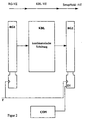
- Figure 3 illustrates the invention.
- the input values E_RG1 and output values A_RG1 from the input register RG1 (at least partially) compared in a comparison unit COM. It can be used to determine whether and where after the next clock edge of the clock signal T a signal value change will occur at the exit.
- the control circuit generates CON1 a signal R with which the loading of the combinatorial Circuit KBL subsequent output register RG2 is controlled depending on signal value changes.
- the signal R from the control circuit CON1 can be used to indicate when or after how many cycles a new value to the input register RG1 can be created.
- Figure 4 shows an application example of the above Invention on an adder ADD between an input register RG1 and an output register RG2 arranged is.
- the input register RG1 has two four-byte inputs OP1, OP2 and a four byte output AG.
- the adder ADD is pure combinatorial structure.
- This "1" is then delayed on the one hand in a circuit DFF, around the enable input EN of the output register RG2 to set to "1", so that with the next clock signal T the value of the output of the adder ADD in the output register RG2 can be saved.
- this value can be as Flag R are output, so that depending on the value on Input of the input register RG1 held another clock can be. In this case, the output of the NOR operation a bar later the value "1" appear, and that Result clocked into register RG2 one clock later will.
Landscapes
- Physics & Mathematics (AREA)
- Engineering & Computer Science (AREA)
- Computer Hardware Design (AREA)
- Computing Systems (AREA)
- General Engineering & Computer Science (AREA)
- Mathematical Physics (AREA)
- Logic Circuits (AREA)
- Executing Machine-Instructions (AREA)
- Manipulation Of Pulses (AREA)
Applications Claiming Priority (2)
| Application Number | Priority Date | Filing Date | Title |
|---|---|---|---|
| DE19639937 | 1996-09-27 | ||
| DE19639937A DE19639937C1 (de) | 1996-09-27 | 1996-09-27 | Schaltungsanordnung mit zwischen Registern angeordneten kombinatorischen Blöcken |
Publications (3)
| Publication Number | Publication Date |
|---|---|
| EP0833451A2 true EP0833451A2 (fr) | 1998-04-01 |
| EP0833451A3 EP0833451A3 (fr) | 1999-10-20 |
| EP0833451B1 EP0833451B1 (fr) | 2004-08-04 |
Family
ID=7807190
Family Applications (1)
| Application Number | Title | Priority Date | Filing Date |
|---|---|---|---|
| EP97115362A Expired - Lifetime EP0833451B1 (fr) | 1996-09-27 | 1997-09-04 | Circuit comportant des blocs combinatoires entres des registres |
Country Status (6)
| Country | Link |
|---|---|
| US (1) | US5999086A (fr) |
| EP (1) | EP0833451B1 (fr) |
| JP (1) | JP3626336B2 (fr) |
| KR (1) | KR19980024989A (fr) |
| DE (2) | DE19639937C1 (fr) |
| TW (1) | TW417356B (fr) |
Families Citing this family (20)
| Publication number | Priority date | Publication date | Assignee | Title |
|---|---|---|---|---|
| US6498817B1 (en) * | 1998-09-30 | 2002-12-24 | Koninklijke Philips Electronics N.V. | Circuit for processing data signals |
| AU9684601A (en) | 2000-10-12 | 2002-04-22 | Univ Rochester | Compositions that inhibit proliferation of cancer cells |
| JP2002198488A (ja) * | 2000-12-25 | 2002-07-12 | Mitsubishi Electric Corp | 半導体集積回路装置および設計方法 |
| US7811992B2 (en) | 2002-02-06 | 2010-10-12 | Stasys Technologies, Inc. | Anti-infarction molecules |
| EP2116604A1 (fr) | 2002-08-05 | 2009-11-11 | University of Rochester | Protéines chimères à domaine de transduction protéique/domaine désaminase, composés associés et utilisations correspondantes |
| EP1874950B1 (fr) | 2005-04-05 | 2015-06-03 | Corning Incorporated | Biocapteurs sans étiquette |
| EP2371843B1 (fr) | 2005-05-19 | 2014-09-17 | THE GOVERNMENT OF THE UNITED STATES OF AMERICA, as represented by the Secretary, Department of Health and Human Services | Épitopes fonctionnels d'antigène psa A de streptococcus pneumoniae et leurs utilisations |
| EP2395076A1 (fr) | 2005-10-14 | 2011-12-14 | MUSC Foundation For Research Development | Ciblage du PAX2 pour l'induction de l'immunité à la tumeur à médiation DEFB1 et le traitement contre le cancer |
| US8080534B2 (en) | 2005-10-14 | 2011-12-20 | Phigenix, Inc | Targeting PAX2 for the treatment of breast cancer |
| EP3034083B1 (fr) | 2006-09-21 | 2020-12-09 | University of Rochester | Oligonucléotides antisens pour le traitement de la dystrophie myotonique |
| EP2104516B1 (fr) | 2006-11-01 | 2015-01-07 | University of Rochester | Méthodes et compositions se rapportant à la structure et à la fonction de apobec3g |
| CA2677665C (fr) | 2007-02-08 | 2019-11-05 | University Of Utah Research Foundation | Procedes et compositions apparentes a l'inhibition d'une entree virale |
| CA2734322A1 (fr) | 2008-08-15 | 2010-02-18 | Georgetown University | Canaux sodiques, maladie, et dosages et compositions apparentees |
| US20120070443A1 (en) | 2008-12-02 | 2012-03-22 | University Of Utah Research Foundation | Pde1 as a target therapeutic in heart disease |
| WO2011022502A1 (fr) | 2009-08-18 | 2011-02-24 | Georgetown University | Compositions d'acide boronique et procédés se rapportant au cancer |
| US20110081293A1 (en) | 2009-10-07 | 2011-04-07 | Sanford-Burnham Medical Research Institute | Methods and compositions related to clot-binding lipid compounds |
| WO2011075725A1 (fr) | 2009-12-18 | 2011-06-23 | Sanford-Burnham Medical Research Institute | Méthodes et compositions associées aux composés de liaison aux caillots |
| JP6205345B2 (ja) | 2011-03-28 | 2017-09-27 | ユニヴァーシティー オブ ユタ リサーチ ファウンデーション | ウイルス侵入の阻害に関する方法および組成物 |
| US12025615B2 (en) | 2017-09-15 | 2024-07-02 | Arizona Board Of Regents On Behalf Of Arizona State University | Methods of classifying response to immunotherapy for cancer |
| EP4038222A4 (fr) | 2019-10-02 | 2023-10-18 | Arizona Board of Regents on behalf of Arizona State University | Procédés et compositions pour identifier des néo-antigènes destinés à être utilisés dans le traitement et la prévention du cancer |
Family Cites Families (5)
| Publication number | Priority date | Publication date | Assignee | Title |
|---|---|---|---|---|
| US4039858A (en) * | 1976-04-05 | 1977-08-02 | Rca Corporation | Transition detector |
| US4706216A (en) * | 1985-02-27 | 1987-11-10 | Xilinx, Inc. | Configurable logic element |
| US5055718A (en) * | 1990-05-11 | 1991-10-08 | Actel Corporation | Logic module with configurable combinational and sequential blocks |
| EP0703530A3 (fr) * | 1994-09-21 | 1996-08-14 | Texas Instruments Inc | Détection de transitions logiques dans un système de traitement de données |
| JPH08241296A (ja) * | 1995-03-06 | 1996-09-17 | Mitsubishi Electric Corp | 半導体集積回路 |
-
1996
- 1996-09-27 DE DE19639937A patent/DE19639937C1/de not_active Expired - Fee Related
-
1997
- 1997-09-02 TW TW086112621A patent/TW417356B/zh not_active IP Right Cessation
- 1997-09-04 DE DE59711822T patent/DE59711822D1/de not_active Expired - Lifetime
- 1997-09-04 EP EP97115362A patent/EP0833451B1/fr not_active Expired - Lifetime
- 1997-09-24 JP JP27639597A patent/JP3626336B2/ja not_active Expired - Fee Related
- 1997-09-26 KR KR1019970048907A patent/KR19980024989A/ko not_active Ceased
- 1997-09-26 US US08/937,992 patent/US5999086A/en not_active Expired - Lifetime
Also Published As
| Publication number | Publication date |
|---|---|
| JP3626336B2 (ja) | 2005-03-09 |
| EP0833451A3 (fr) | 1999-10-20 |
| DE19639937C1 (de) | 1998-03-12 |
| US5999086A (en) | 1999-12-07 |
| JPH10124170A (ja) | 1998-05-15 |
| TW417356B (en) | 2001-01-01 |
| KR19980024989A (ko) | 1998-07-06 |
| DE59711822D1 (de) | 2004-09-09 |
| EP0833451B1 (fr) | 2004-08-04 |
Similar Documents
| Publication | Publication Date | Title |
|---|---|---|
| DE19639937C1 (de) | Schaltungsanordnung mit zwischen Registern angeordneten kombinatorischen Blöcken | |
| DE69325321T2 (de) | Unterbrechungsvorrichtung für allgemeines Ein-/Ausgangstor | |
| EP0687363B1 (fr) | Procede de controle d'appareils electroniques de commande | |
| DE69229324T2 (de) | Arithmetik-Logik-Einheit | |
| DE3228405A1 (de) | Emulator zur erzeugung einer folge von steuersignalen | |
| DE3587446T2 (de) | Signalverarbeitungsprozessor und hierarchische Multiverarbeitungstruktur mit mindestens einem solchen Prozessor. | |
| DE3307194C2 (fr) | ||
| DE3700800C2 (de) | Einrichtung zur Erzeugung eines Unterbrechungspunktes in einem Mikroprozessor | |
| CH657487A5 (de) | Funktionsgenerator zur erzeugung einer anzahl von sich wiederholenden digitalen wellenformen. | |
| DE2747304A1 (de) | Einrichtung zur mikrobefehlssteuerung | |
| DE69500544T2 (de) | Mikrocomputer mit integrierter Haltepunktanordnung zur Erkennung von zusammengesetzten Ereignissen | |
| EP0829803B1 (fr) | Processeur de traitement de signal numérique et méthode pour effectuer une multiplication dans un tel processeur | |
| DE19639935C1 (de) | Schaltungsanordnung mit zwischen Registern angeordneten kombinatorischen Blöcken | |
| DE2622140C3 (de) | Einrichtung zur Steuerung manueller Operationen | |
| DE102005020656A1 (de) | Flankenerfassungsschaltung für Leistungszähler | |
| EP0433315A1 (fr) | Circuits d'addition ou de soustraction d'operandes codes selon un code bcd ou dual | |
| DE69220522T2 (de) | Bidirektionaler Boundary-Scan-Schaltkreis | |
| EP0051154A1 (fr) | Procédé et dispositif pour la combinaison d'opérandes de longueur variable dans des systèmes de traitement de données | |
| DE10254653B4 (de) | Vorrichtung zur Steuerung der Verarbeitung von Datenwörtern eines Datenstroms | |
| DE3726659C2 (de) | Schaltungsanordnung zur Erweiterung der Anschlußmöglichkeiten für mit einer zentralen Steuereinrichtung zusammenarbeitende periphere Einheiten | |
| DE19910620C2 (de) | Vorrichtung zur Durchführung von Rechenvorgängen | |
| DE69227744T2 (de) | Teilmultiplikatorselektor für Multiplikationsschaltung | |
| DE2922234C2 (de) | Verfahren und Schaltungsanordnung zur Bereitstellung von logischen Verknüpfungsergebnissen in datenverarbeitenden Einrichtungen | |
| DE4312090C2 (de) | Digitalprozessor | |
| EP0195284A2 (fr) | Dispositif de comptage du nombre de bits 1/0 contenus dans un mot binaire de n-bits |
Legal Events
| Date | Code | Title | Description |
|---|---|---|---|
| PUAI | Public reference made under article 153(3) epc to a published international application that has entered the european phase |
Free format text: ORIGINAL CODE: 0009012 |
|
| AK | Designated contracting states |
Kind code of ref document: A2 Designated state(s): DE FR GB IT |
|
| PUAL | Search report despatched |
Free format text: ORIGINAL CODE: 0009013 |
|
| RIC1 | Information provided on ipc code assigned before grant |
Free format text: 6H 03K 19/096 A, 6H 03K 19/017 B, 6G 06F 9/38 B |
|
| AK | Designated contracting states |
Kind code of ref document: A3 Designated state(s): AT BE CH DE DK ES FI FR GB GR IE IT LI LU MC NL PT SE |
|
| 17P | Request for examination filed |
Effective date: 19991118 |
|
| AKX | Designation fees paid |
Free format text: DE FR GB IT |
|
| RAP1 | Party data changed (applicant data changed or rights of an application transferred) |
Owner name: INFINEON TECHNOLOGIES AG |
|
| GRAP | Despatch of communication of intention to grant a patent |
Free format text: ORIGINAL CODE: EPIDOSNIGR1 |
|
| RIC1 | Information provided on ipc code assigned before grant |
Ipc: 7G 06F 9/38 B Ipc: 7H 03K 19/017 B Ipc: 7H 03K 19/096 A |
|
| RTI1 | Title (correction) |
Free format text: CIRCUIT COMPRISING COMBINATORY LOGIC BLOCKS BETWEEN REGISTERS |
|
| GRAS | Grant fee paid |
Free format text: ORIGINAL CODE: EPIDOSNIGR3 |
|
| GRAA | (expected) grant |
Free format text: ORIGINAL CODE: 0009210 |
|
| AK | Designated contracting states |
Kind code of ref document: B1 Designated state(s): DE FR GB IT |
|
| PG25 | Lapsed in a contracting state [announced via postgrant information from national office to epo] |
Ref country code: IT Free format text: LAPSE BECAUSE OF FAILURE TO SUBMIT A TRANSLATION OF THE DESCRIPTION OR TO PAY THE FEE WITHIN THE PRESCRIBED TIME-LIMIT;WARNING: LAPSES OF ITALIAN PATENTS WITH EFFECTIVE DATE BEFORE 2007 MAY HAVE OCCURRED AT ANY TIME BEFORE 2007. THE CORRECT EFFECTIVE DATE MAY BE DIFFERENT FROM THE ONE RECORDED. Effective date: 20040804 Ref country code: GB Free format text: LAPSE BECAUSE OF FAILURE TO SUBMIT A TRANSLATION OF THE DESCRIPTION OR TO PAY THE FEE WITHIN THE PRESCRIBED TIME-LIMIT Effective date: 20040804 Ref country code: FR Free format text: LAPSE BECAUSE OF FAILURE TO SUBMIT A TRANSLATION OF THE DESCRIPTION OR TO PAY THE FEE WITHIN THE PRESCRIBED TIME-LIMIT Effective date: 20040804 |
|
| REG | Reference to a national code |
Ref country code: GB Ref legal event code: FG4D Free format text: NOT ENGLISH |
|
| REF | Corresponds to: |
Ref document number: 59711822 Country of ref document: DE Date of ref document: 20040909 Kind code of ref document: P |
|
| GBV | Gb: ep patent (uk) treated as always having been void in accordance with gb section 77(7)/1977 [no translation filed] |
Effective date: 20040804 |
|
| PLBE | No opposition filed within time limit |
Free format text: ORIGINAL CODE: 0009261 |
|
| STAA | Information on the status of an ep patent application or granted ep patent |
Free format text: STATUS: NO OPPOSITION FILED WITHIN TIME LIMIT |
|
| 26N | No opposition filed |
Effective date: 20050506 |
|
| EN | Fr: translation not filed | ||
| PGFP | Annual fee paid to national office [announced via postgrant information from national office to epo] |
Ref country code: DE Payment date: 20151119 Year of fee payment: 19 |
|
| REG | Reference to a national code |
Ref country code: DE Ref legal event code: R119 Ref document number: 59711822 Country of ref document: DE |
|
| PG25 | Lapsed in a contracting state [announced via postgrant information from national office to epo] |
Ref country code: DE Free format text: LAPSE BECAUSE OF NON-PAYMENT OF DUE FEES Effective date: 20170401 |