EP0833442B1 - Rausch- und Impedanzangepasste integrierte Hochfrequenzschaltkreise - Google Patents
Rausch- und Impedanzangepasste integrierte Hochfrequenzschaltkreise Download PDFInfo
- Publication number
- EP0833442B1 EP0833442B1 EP97307266A EP97307266A EP0833442B1 EP 0833442 B1 EP0833442 B1 EP 0833442B1 EP 97307266 A EP97307266 A EP 97307266A EP 97307266 A EP97307266 A EP 97307266A EP 0833442 B1 EP0833442 B1 EP 0833442B1
- Authority
- EP
- European Patent Office
- Prior art keywords
- noise
- transistor
- impedance
- input
- transistors
- Prior art date
- Legal status (The legal status is an assumption and is not a legal conclusion. Google has not performed a legal analysis and makes no representation as to the accuracy of the status listed.)
- Expired - Lifetime
Links
Images


Classifications
-
- H—ELECTRICITY
- H03—ELECTRONIC CIRCUITRY
- H03F—AMPLIFIERS
- H03F1/00—Details of amplifiers with only discharge tubes, only semiconductor devices or only unspecified devices as amplifying elements
- H03F1/08—Modifications of amplifiers to reduce detrimental influences of internal impedances of amplifying elements
- H03F1/22—Modifications of amplifiers to reduce detrimental influences of internal impedances of amplifying elements by use of cascode coupling, i.e. earthed cathode or emitter stage followed by earthed grid or base stage respectively
-
- H—ELECTRICITY
- H03—ELECTRONIC CIRCUITRY
- H03F—AMPLIFIERS
- H03F1/00—Details of amplifiers with only discharge tubes, only semiconductor devices or only unspecified devices as amplifying elements
- H03F1/26—Modifications of amplifiers to reduce influence of noise generated by amplifying elements
-
- H—ELECTRICITY
- H03—ELECTRONIC CIRCUITRY
- H03F—AMPLIFIERS
- H03F1/00—Details of amplifiers with only discharge tubes, only semiconductor devices or only unspecified devices as amplifying elements
- H03F1/56—Modifications of input or output impedances, not otherwise provided for
- H03F1/565—Modifications of input or output impedances, not otherwise provided for using inductive elements
-
- H—ELECTRICITY
- H03—ELECTRONIC CIRCUITRY
- H03F—AMPLIFIERS
- H03F3/00—Amplifiers with only discharge tubes or only semiconductor devices as amplifying elements
- H03F3/189—High-frequency amplifiers, e.g. radio frequency amplifiers
-
- H—ELECTRICITY
- H03—ELECTRONIC CIRCUITRY
- H03F—AMPLIFIERS
- H03F2200/00—Indexing scheme relating to amplifiers
- H03F2200/294—Indexing scheme relating to amplifiers the amplifier being a low noise amplifier [LNA]
-
- H—ELECTRICITY
- H03—ELECTRONIC CIRCUITRY
- H03F—AMPLIFIERS
- H03F2200/00—Indexing scheme relating to amplifiers
- H03F2200/372—Noise reduction and elimination in amplifier
-
- H—ELECTRICITY
- H03—ELECTRONIC CIRCUITRY
- H03F—AMPLIFIERS
- H03F2200/00—Indexing scheme relating to amplifiers
- H03F2200/489—A coil being added in the source circuit of a common source stage, e.g. as degeneration means
-
- H—ELECTRICITY
- H03—ELECTRONIC CIRCUITRY
- H03F—AMPLIFIERS
- H03F2200/00—Indexing scheme relating to amplifiers
- H03F2200/492—A coil being added in the source circuit of a transistor amplifier stage as degenerating element
Definitions
- This invention relates to high frequency noise and impedance matched integrated circuits and a methodology for circuit design, with particular application to silicon integrated circuits using integrated inductors for RF circuit applications.
- Recent developments in broadband multimedia communications systems are based on wireless asynchronous transfer mode (ATM) transmission in the 5GHz band.
- ATM wireless asynchronous transfer mode
- GaAs circuits remain several times more expensive than silicon circuits, the feasibility of using lower cost silicon based technology in this frequency band has been limited, due to significantly higher substrate and interconnect losses in silicon relative to GaAs.
- silicon technology has suffered from a lack of high Q inductors. More recently, improved inductor performance has been obtained using microstrip transmission line inductors.
- a passive network is designed around a given transistor in order to achieve noise matching and/or impedance matching.
- the passive network itself contributes losses and degrades the noise figure, as discussed by F. McGrath et al, in "A 1.9GHz GaAs Chip set for the personal handyphone system", IEEE Trans. MTT Vol. 43, pp. 1733-1744, 1995 and by A. Brunel, et al. in "A Downconverter for use in a dual mode AMPS/CDMA chip set", in Microwave J., pp. 20-42, February 1996.
- the losses in the passive network increase as the network become more complicated, and a significant area of an integrated circuit may be taken up by the matching network.
- the noise figure or input impedance matching are sub-optimal, or the passive matching circuit is excessively complex, occupying a large semiconductor area.
- GaAs circuits are at least a factor of two more expensive than silicon circuits. Consequently, if matching losses were reduced for silicon substrates to allow for design of high performance wireless circuits, these circuits could be fabricated in silicon with significant cost savings relative to similar GaAs circuits.
- the present invention seeks to provide improved noise and impedance matching for monolithic integrated circuits, particularly for silicon integrated circuits for high frequency applications in RF and wireless technology, and a design methodology for integrated circuits, which overcomes or avoids the above mentioned limitations.
- the invention provides an integrated circuit as defined in claim 1 and a method for providing a noise and impedance matched double balanced mixer or low noise differential amplifier as claimed in claim 7.
- an integrated circuit including an integrated transistor-inductor structure, the structure comprising:
- the noise and impedance matched integrated circuit structure comprising an optimised integrated-transistor-inductor structure provides improved performance at high frequencies suitable for RF and wireless circuit applications such as telecommunications.
- the characteristic impedance of the system Z 0 is 50 ⁇ .
- Z 0 may be increased from the typical 50 ⁇ , if required, in order to improve performance further.
- the integrated circuit comprises a bipolar transistor comprising an emitter, base and collector, coupled in common emitter configuration
- the length l E of the emitter is optimized to provide noise matching of the transistor
- the first inductor is an emitter coupled inductor LE for matching the real part of the input impedance Z 0
- the second inductor is a base coupled inductor L B for matching the imaginary part of the input impedance and noise reactance to 0 ⁇ .
- the width w G of the gate is optimized to provide noise matching of the transistor
- the first inductor is a source coupled inductor L E for matching the real part of the input impedance Z 0
- the second inductor is a gate coupled inductor L B for matching the imaginary part of the input impedance and noise reactance to 0 ⁇ .
- a second transistor Q2 is added for input/output buffering, the second transistor being coupled to the first transistor in cascode configuration, and size ratio of Q1 to Q2 being determined by the ratio of the peak f T current density and the minimum noise current density.
- an integrated circuit including an integrated transistor-inductor structure, the structure comprising:
- the emitter length l E2 of the second transistor is selected to provide that it is biased at the current density at which its cutoff frequency reaches a maximum for maximizing gain and frequency of operation.
- the size ratio, i.e. the ratio of the emitter lengths, of the first and second transistors is determined by the ratio of the peak fT current density to the minimum noise current density.
- the design of the transistor-inductor structure is based on a novel approach to design methodology in which the size of the transistor is designed first so that real part of the optimum noise impedance of the transistor is noise matched to the characteristic impedance of the system Z 0 , typically 50 ⁇ , at the desired frequency and collector current density. Since the transistor is an active device, noise matching is achieved without losses and without noise figure degradation. The task of noise matching of the transistor is thus removed from the passive network. Losses in the passive network around the transistor are reduced, and the resulting matching network is therefore simpler, and less lossy than in current known circuit designs.
- a minimal passive network comprising only two lossless inductors is designed to provide impedance matching with the lowest possible degradation of the overall noise figure.
- the simplified matching network reduces components and saves area, contributing to significant cost reduction.
- the noise and impedance matched transistor-inductor structure may be used to build integrated circuits such as low noise amplifiers and mixer circuits with significantly improved performance at high frequencies. Performance of noise and impedance matched silicon transistor-inductor devices has been obtained which is comparable to that of GaAs at frequencies in the 1 to 12 GHz range.
- the noise matched transistor-inductor structure may provide a circuit operable as a low noise amplifier, comprising: means for supplying a first input signal coupled to the first transistor base through the second inductor L B2; the transistor emitter coupled to an emitter degeneration means comprising the first inductor L E; and output means coupled to the collector of the first transistor for generating an output signal.
- the transistor-inductor structure may be used to provide a circuit operable as a mixer, comprising: means for supplying an first input (RF) signal coupled to the first transistor base through the second inductor L B ; a second base inductor coupled to the base of the second transistor and means for supplying a second input (LO) signal coupled to the second transistor through the second base inductor; the transistor emitter coupled to an emitter degeneration means comprising the first inductor L E, for generating an output (IF) signal at output means coupled to the collector of the first transistor.
- Each transistor may, for example, be a bipolar transistor selected from the group consisting bipolar junction transistors (BJTs) or heterojunction bipolar transistors (HBTs).
- the transistors may be field effect transistors, i.e. silicon MOSFETs or MESFETs, JFETs, and HEMT transistors.
- the noise and impedance matched circuits may be implemented, for example, in silicon, silicon germanium, or a III-V compound semiconductor.
- the simple and compact integrated transistor-inductor structure is used to demonstrate the feasibility of fabricating a cost effective, high performance, high speed silicon integrated circuit, which is simultaneously noise and impedance matched.
- a silicon integrated circuit comprising a integrated transistor-inductor structure for operation as a double balanced mixer, comprising:
- the size ratio of the transistors in the mixing quad and the input pair is based on ratio of the peak f T current density and the minimum noise current density.
- the circuit includes an LO reject filter comprising an series LC filter coupled between the differential IF outputs, and a parallel LC resonator tuned on the second RF harmonic as an AC current source coupled in the emitter of the input pair.
- a silicon integrated circuit comprising a transistor-inductor structure for operation as a low noise differential amplifier, comprising:
- the emitter lengths of the first and second pairs of transistors are characterized by being twice as large as the corresponding emitter lengths in the corresponding single ended circuit.
- the integrated transistor-inductor structure may be used to advantage in providing various input impedance and noise matched low noise amplifier circuit and a mixer circuit of simple and compact design.
- the circuits may be implemented in silicon, and provide high frequency performance more generally found only in GaAs circuits.
- These structures may be fabricated by known silicon process technology, and implemented in either high speed silicon bipolar or silicon MOSFET technologies.
- Other high speed silicon based devices, for example SiGe bipolar transistors may alternatively be used.
- monolithic silicon low noise amplifier and a mixer circuits operable at 5.8 GHz are demonstrated to be feasible with performance characteristics previously reported only for GaAs based circuits.
- This improved performance at a record high frequency for a silicon based circuit is dependent on several factors.
- the unconventional design methodology presented herein in which the transistor emitter length is treated as a design variable. Initially, the transistor emitter length is optimised to obtain noise matching, which then allows a very much simplified matching network.
- the use of a high performance silicon bipolar technology takes advantage of recent improvements in inductors and microstrip transmission lines using multilevel metallization schemes. The latter benefit from use of first level metal as ground planes to reduce substrate losses.
- the structure is also beneficial in avoiding the trade-off in noise and input impedance matching in designing GaAs and other III-V compound semiconductors to obtain optimal performance.
- Another example provides a method for providing a noise and impedance matched integrated circuit comprising an integrated transistor-inductor structure, comprising:
- the design is achieved in two stages, I) the noise matched transistor design stage, which optimises noise matching at a selected frequency, and II) the circuit design stage in which simultaneous impedance and noise matching is pursued.
- the transistor has a characteristic dimension, the characteristic dimension being an emitter length l E for a bipolar transistor and a gate width w g for field effect transistor, which is designed to provide that the real part of its optimum noise impedance is equal to the characteristic impedance of the system, Z 0 .
- Designing a minimal passive impedance matching circuit comprises determining the inductance of an emitter inductor L E to match the real part of the input impedance to Z 0 , and then, determining the inductance of a base inductor L B to simultaneously match the imaginary part of the input impedance and the noise impedance to 0 ⁇ .
- This design approach is unique in treating the transistor geometry as a design variable.
- a characteristic dimension of the transistor i.e. the emitter length of a bipolar transistor, or the gate width of a field effect transistor is optimised to achieve noise matching of the transistor.
- the design methodology allows for simultaneous optimization of both the transistor parameters and the passive matching network component parameters.
- the optimal noise current density is determined by using F MIN vs. log(I C ) curves.
- the design is carried out using a commercially available design tool such as HSPICETM.
- the scalable models provide analytical equations for determination of the noise and impedance parameters of the transistors and passive components using a standard design tool. These equations were used to develop customised input decks for HSPICE to derive the required design parameters. Sample input decks developed for HSPICE for either bipolar transistors or MOSFETs are included in Appendices A and B, respectively. Alternatively appropriately customised decks to solve the equations may be created for other design tools. Thus optimized performance is readily obtainable with commercially available or custom design tools.
- optimized noise and impedance matching of an integrated circuit is achieved in a integrated circuit of simple design by a two stage design approach providing a noise optimized transistor and a minimal inductor network for impedance matching.
- Part of a monolithic silicon integrated circuit 10 comprising an integrated transistor-inductor structure 12 according to a first example is shown schematically in Figure 1, and comprises a first transistor 14, which is a common emitter bipolar transistor Q 1 for low noise amplification, and a second transistor 16, which is a common base transistor Q 2 for input/output buffering, the two transistors being coupled in cascode configuration; a first inductor 18 L E is coupled to the emitter 20 of the first transistor Q 1 ; and, a second inductor 22 L B coupled to the base 24 of the first transistor Q 1.
- Noise and impedance matching of the transistor-inductor structure is achieved by designing the transistor 14 having an specific geometry, and in particular a specific emitter length l E , which provides that the real part of its optimum noise impedance at the desired frequency of operation and collector current density is equal to the characteristic impedance Z 0 of the system, i.e. the integrated circuit.
- design of the matching network is reduced to adding a very simple passive matching network using only two inductors.
- the first inductor 18, L E provides matching of the real part of the input impedance, and the second inductor 22, L B cancels out the noise reactance and input impedance reactance of the structure.
- the size ratio of the emitter lengths of the first and second transistors is determined by the ratio of the f T current density to the minimum noise current density. In the circuit represented in Figure 1, the ratio is 8 to 1, which is technology dependent.
- an integrated transistor-inductor structure comprising a transistor Q1 having an emitter length l E designed to provide noise matching at a desired operating frequency, and a simplified matching network of two inductors L E and L B of the appropriate values to provides impedance matching of the circuit, provides a simultaneously noise and impedance matched circuit.
- This structure is particularly advantageous in optimising performance of silicon based circuits for wireless and RF applications.
- the design of the transistor-inductor structure is based on a design methodology, i.e. a method of designing an integrated circuit, which will be described in detail in the following section, and in which the geometry of the transistor is determined by design, i.e. considered to be a variable rather than fixed design parameter. That is, the emitter length of a bipolar transistor, or correspondingly, the gate width of a field effect transistor (FET), is adjusted so that the transistor is noise matched to the characteristic impedance of the system, typically 50 ⁇ , at the desired operating frequency, thereby minimizing the losses in the passive network around the transistor. Since the transistor is an active device, noise matching is achieved without losses and without noise figure degradation. The task of noise matching is thus removed from the passive network. The resulting matching network is therefore simpler, and less lossy than in presently known circuit designs.
- a design methodology i.e. a method of designing an integrated circuit, which will be described in detail in the following section, and in which the geometry of the transistor is determined by design, i.e. considered
- a minimal passive network comprising two lossless integrated inductors is designed to provide impedance matching with the lowest possible degradation of the overall noise figure.
- the minimal matching network reduces components and saves area, and therefore contributes to significant cost reduction.
- the noise resistance and the optimum noise admitttance scale as l E and l E -1 , respectively.
- F MIN of the transistor is invariant to changes in emitter length provided that the length to width ratio l E /w E of the emitter stripe is greater than 10.
- All noise parameters are non-linear functions of emitter width, w E through the I C (r E + r B ) term.
- the ability to predict the impact of the statistical emitter width and length variations on the noise parameters depends on the availability of a physically based, scalable compact model.
- l E1, J Q1, L E and L B For the combination of the first transistor and the two inductors, a unique combination of l E1, J Q1, L E and L B is determined that leads to a structure with minimum noise figure F MIN and ideal input impedance match. While the second transistor is optional and may be omitted, for practical purposes the second transistor is included in order to maximize the power gain and the frequency of operation.
- the size of the second transistor Q2 is selected such that it is biased at the current density at which its cut-off frequency reaches a maximum. The size ratio of Q1 to Q2 depends on the ratio of the peak f T current density to the minimum noise current density.
- the design of a noise and impedance matched circuit is achieved in two stages, I) the noise matched transistor design stage and II) the circuit design stage in which simultaneous impedance and noise matching is pursued.
- the first stage of the design process involves finding the optimal noise current density, from an analytic equation as set out below, using a commercial design tool, i.e. HSPICE.
- the noise parameter equations set out in the references, in analytical format were entered in an HSPICE simulator input deck to compute simultaneously the minimum noise figure F MIN , the cut-off frequency f T , maximum oscillation frequency f MAX , noise resistance R n , and optimum source admittance Y SOP as functions of the transistor collector current I C for a bipolar transistor, (or correspondingly, as functions of transistor drain current I D when a MOSFET transistor is to be considered).
- Corresponding sample HSPICE decks for a bipolar and MOSFET transistor are given in the appendices A and B respectively.
- the optimal noise current density J Q1 is obtained from equation (1) using an HSPICE deck, as represented in Figure 4, which shows graphically the dependence of F MIN , f T and f max on the collector current. From this data, the optimal noise current density J Q1 is determined for the desired operating frequency. Since R sop is a function of l E , the emitter length, this parameter is adjusted so that the optimum source resistance R SOP equals the characteristic impedance of the system Z 0 (50 ⁇ ) at the minimum noise current density and at frequency f, as expressed in equation (2), which is represented graphically in Figure 5.
- the transistor size, specifically l E and bias current are determined.
- the optimum noise impedance of the transistor at the end of the first stage is shown plotted on a Smith chart in Figure 6.
- an emitter inductor L E is added to match the real part of the input impedance to Z 0 as shown in Figure 7, and defined by equation (3) as a function of the frequency f T .
- L E does not change the value of R SOP but it does affect the source reactance X SOP which is defined by equation (4).
- simultaneous noise and input impedance matching is obtained by connecting an inductor L B in the base of the transistor Q1 as shown in Figure 8. This inductor cancels out the reactance due to the input capacitance, C in , of the device, and at the same time, it transforms the optimum noise reactance of the amplifier to 0 ⁇ .
- L B is defined by equation (5).
- this design methodology ensures that the real part of the optimum noise impedance of the transistor is equal to the characteristic impedance Z 0 at desired frequency and collector current density.
- Optimal noise and input impedance matching is achieved with the simplest matching network.
- a suitable matching network in the collector may be added to maximize the power gain.
- the scaleable model allows for the transistor size to be uniquely dimensioned in order to achieve optimal noise matching. The optimal transistor size and bias current decrease with increasing frequency.
- test structures with emitter inductors only, and with both base and emitter inductors were fabricated in a proprietary Northern Telecom silicon bipolar process (NT25) at 1.9, 2.4 and 5.8 GHz.
- NT25 Northern Telecom silicon bipolar process
- test structures were fabricated with various emitter widths, lengths, and single and multistripe geometries. Agreement between measured parameters and Spice Gummel Poon modelled parameters were well within the typical on wafer noise measurement error.
- Part 40 of a monolithic silicon integrated circuit operable as a differential amplifier according to a first embodiment of the present invention is shown schematically in Figure 2.
- This circuit is the differential equivalent of the single ended amplifier structure 10 shown in Figure 1.
- the circuit 40 comprises an input pair 42 and 44 of common emitter bipolar transistors Q1 and Q2 for low noise amplification, and an output pair 46 and 48 of common base bipolar transistors Q3 and Q4 for input/output buffering, the two pairs being coupled in cascode configuration.
- Inputs for supplying differential RF signals RF N and RF P are coupled to the bases of the input pair Q1 and Q2, and differential output signals OUT P and OUT N generated at outputs coupled to the collectors of output pair Q3 and Q4.
- Matching of the real part of the noise impedance of the input pair of transistors Q1 and Q2 is achieved as described for the single ended structure of the first embodiment, by design of the transistors Q1 and Q2 with appropriate an emitter length to make the real part of its optimum noise impedance at the desired frequency of operation and collector current density equal to the characteristic impedance Z 0 .
- Emitter inductors 50 and 52 provide matching of the real part of the input impedance and base inductors 54 and 56, L B and L B ', cancel out the noise reactance and input impedance reactance of the structure, as described for the structure of the first example, to complete noise and impedance matching.
- the ratio of the sizes of the first and second pairs of transistors i.e.
- emitter lengths of the Q1 and Q2, relative to the emitter lengths of Q3 and Q4, is by the ratio of the peak f T current density to the minimum noise current density, as determined for the single ended amplifier.
- the emitter lengths of Q3 and Q4 are 1/8 of the emitter length l E D of the input pair Q1 and Q2, or as shown in Figure 2, as l E /4 where l E is the emitter length of the input transistor of the corresponding single ended circuit shown in Figure 1.
- Part of a monolithic silicon integrated circuit 100 operable as a mixer circuit and comprising an integrated transistor-inductor structure 110 according to a second example is shown schematically in Figure 3, and comprises a first transistor 112, which is a common emitter bipolar transistor Q1 for low noise amplification, and a second transistor 114, which is a common base transistor Q 2 for mixing, the two transistors being coupled in cascode configuration; a first inductor 116 L E is coupled to the emitter 118 of the first transistor Q1; and, a second inductor 120 L B coupled to the base 122 of the first transistor Q1.
- noise and input impedance matching of the transistor-inductor structure is achieved by designing the transistor 112 having an specific geometry, and in particular a specific emitter length l E , which provides that the real part of its optimum noise impedance at the desired frequency of operation and collector current density is equal to the characteristic impedance Z 0 of the system, i.e. the integrated circuit.
- the first inductor L E provides matching of the real part of the input impedance
- the second inductor L B cancels out the noise reactance and input impedance reactance of the structure.
- the size ratio of the transistor Q1 and Q2, i.e. the ratio of the emitter lengths of the first and second transistors, is determined by the ratio of the peak f T current density to the minimum noise current. In this example the emitter length ratio was 8:1, which is technology dependent.
- two silicon integrated circuits were designed, a double balanced mixer and a low noise amplifier, for application in a 5.8 GHz down-converter.
- the two circuits were designed to be simultaneously noise and impedance matched at the RF input, and were fabricated in a proprietary Northern Telecom 25GHz silicon bipolar process technology (NT25) using implanted base, double polysilicon transistors, inductors, and microstrip transmission lines.
- NT25 Northern Telecom 25GHz silicon bipolar process technology
- the three layer metallization with 2 ⁇ m thick aluminum top metal layer allows for the fabrication of inductors with Q's in the 6-10 range, and of metal 1 grounded microstrip lines with Qs of 6, at 26 GHz.
- F MIN is typically 2 dB at 5.8GHz and BV CE0 and BV CB0 are 4.2V and 15V respectively.
- FIG. 9 A schematic of the core of a silicon double balanced mixer circuit according to a second embodiment of the present invention is shown in Figure 9.
- the circuit is a development based on a CDMA GaAs MESFET mixer architecture described in the Brunel reference, which is is a modified Gilbert cell mixer incorporating an inductor/capacitor/resistor matching network.
- the circuit shown in Figure 9 differs in incorporating the noise and impedance matched transistor-inductor structure, which simplifies the matching network, as described above, and allows for implementation in silicon with performance comparable to GaAs at 5.8GHz.
- the mixer comprises an input pair of common emitter transistors Q1 and Q2, each coupled to respective common source differential pairs Q3,Q4 and Q5, Q6 which form a mixing quad.
- An RF IN signal is coupled to the base of the transistor Q1, and the base of the transistor Q2 is AC grounded.
- Differential LO inputs are coupled to the bases of differential pairs of the mixing quad to generate differential IF output signals at outputs coupled to collectors of the pairs the mixing quad.
- the emitter lengths of Q1 and Q2 are designed to provide matching of the real part of the noise impedance, and first and second inductors provide a passive matching network, as described above.
- the emitter inductors L E and L E ' provide matching of the real part of the input impedance to Z 0
- the base inductor L B provides for cancelling the imaginary part of the input impedance and the noise reactance. Since one of the RF inputs is AC grounded, a single base inductor L B only is required.
- the mixer also features an LO reject, series LC filter between the differential IF outputs, and a parallel LC resonator, tuned on the second RF harmonic, as an AC current source in the emitter of the input pair.
- Inductors L E and L E ' replace conventional resistors for emitter degeneration.
- the inductors alleviated to a large degree the trade off between IIP3 and the noise figure.
- Z 0 can usually be increased from the typical 50 ⁇ , if required, in order to further improve IIP3.
- a silicon low noise amplifier (LNA) circuit according to a third example is shown in Figure 10, and has an architecture similar to that usually implemented in GaAs circuits.
- the circuit differs in that it incorporates the simultaneously noise and impedance matched transistor-inductor structure comprising bipolar transistor Q1, and inductors L E and L B , as described in the first embodiment, and is implemented in silicon for operation at 5.8 Ghz.
- the first transistor Q 1 is a 2x0.5*20 m 2 bipolar device, biased at a minimum noise current of 2.2mA.
- This is different from the mixer circuit of the second embodiment, which is fully differential. It can be demonstrated that the minimum noise figure of a differential stage is identical to that of the half circuit and that the optimum noise impedance is two times larger.
- the size of each of the transistors in the input pair of the double balanced mixer of Figure 9 is 4x0.5*20 ⁇ m 2 and bias current is 4 mA, roughly twice those of the LNA ( Figure 10). Both circuits are noise and input impedance matched to 50 ⁇ .
- the size of the transistors in the mixing quad was chosen 8 times smaller than that of the input pair, as indicated in the basic transistor-inductor structure shown in Figure 1.
- the size ratio corresponds to the ratio of the peak f T current density and the minimum noise current density.
- a similar approach is used for common base transistor Q2 in the LNA to increase gain by 1 to 2 dB.
- FIG. 14 and 15 Schematic layouts of the integrated circuits for the LNA and double balanced mixer circuits are shown in Figures 14 and 15. Corresponding photomicrographs of the actual integrated circuit layouts, on a reduced scale, are shown in Figures 14A and 15A. 50 ⁇ microstrip transmission lines with metal 1 ground planes were used at the local oscillator inputs, in order to minimize substrate losses and to provide a controlled and dispersion free transmission medium.
- the measured performance of the LNA and double balanced mixer are summarized in Table 1 for operation at 5.8 GHz.
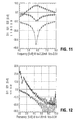
- the gain and input return loss of the LNA mixer are shown in Figure 11 and 12 respectively.
- the noise figure for the 5.8 GHz LNA is plotted vs. frequency in Figure 13.
- the conversion gain of the mixer was measured with a noise figure meter and was confirmed with S parameter measurements with the mixer biased as an amplifier with dc LO inputs only.
- mixer and LNA circuits were based on silicon bipolar transistors.
- these circuits may be implemented using silicon MOSFET transistors.
- the scalable model for bipolar transistors mentioned above is adaptable to silicon MOSFETs.
- the scalable MISNAN model developed by Northern Telecom Limited is employed.
- the LNA and mixer circuits described herein are the first fully integrated silicon based mixer and low noise amplifier circuits which have been demonstrated to be operable at 5.8Ghz, with performance which has previously only been achieved using GaAs based circuits. Moreover, the circuits occupy a record small area for a LNA and a mixer circuit, and provide a factor of at least two in cost reduction relative to a comparable GaAs implementation delivering similar performance.
- the noise and impedance matched inductor-transistor structure may also be used for other RF and wireless circuits.
- RF radio frequency
- MMICs microwave monolithic integrated circuits
- test results showed improved performance when the scalable model was applied to the design of silicon based Darlington amplifiers having 16dB gain, 7.1GHz bandwidth and 8dB gain 12.6 GHz bandwidth, the layouts of which are shown schematically in Figures 16 and 17.
- Corresponding photomicrographs of the chip layout on a reduced scale are shown in Figures 16A and 17A. These circuits would have potential applications in broadband optical fiber transmission at 10 Gb/s and 17.5 Gb/s respectively.
- the size of the output transistor was selected to meet the output compression point specification whereas the input transistor length was optimized to reduce the group delay ripple within the 3 dB bandwidth by adjusting the Q of the resonant circuit associated with the negative resistance of the emitter-follower.
- the gain input return loss and group delay are plotted in Figures 18 and 19 as functions of frequency for the 12.6 GHz bandwidth Darlington amplifier.
- the noise figure of the 7.1 GHz Darlington amplifier is 5.7 dB at 2 GHz increasing to 8.17 dB at 7 GHz.
- the 12.6 GHz Darlington amplifier has a noise figure of 7.1 dB and 12.5 dB at 2 GHz and 12 GHz respectively.
- Gain and bandwidth variation across the wafer for the 8 dB gain amplifier was better than 0.8 dB and 1GHz respectively.
- the design methodology for the noise and input impedance matched transistor-inductor structure is based on two key features.
- the transistor geometry is treated as a design variable to achieve matching of the real part of the noise impedance of the transistor to the characteristic impedance at the desired frequency, i.e. by adjusting the emitter length or gate width.
- This approach is in contrast to conventional designs in which the transistor dimensions (size) are treated as fixed parameters.
- the transistor size is selected initially to suit the application.
- a minimal passive network is then designed around the noise matched transistor. Again, this contrasts with the conventional approach in which a relative complex passive network is required to provide noise and impedance matching.
- a conventional matching network is therefore considerably more lossy and occupies a much larger area than the relatively simple matching network resulting from the methodology described herein.
- Circuit performance is optimized using fewer components, and the integrated circuit chip area is reduced, both factors being significant cost drivers in integrated circuit manufacturing.
- the transistor size for optimal noise match depends on operating frequency and bias current density, whether the circuit is implemented in silicon bipolar technology, i.e. either bipolar junction transistors (BJTs) or Heterojunction bipolar transistors (HBTs); or field effect transistors, MOSFET, MESFET, JFET, HEMT. Sample HSPICE input decks for both bipolar and MOSFET transistors may be adapted for these transistors.
- the design methodology is particularly applicable to optimising noise and input impedance to reduce losses significantly, and obtain optimal performance in integrated circuits designed in silicon or using heterostructures such as silicon-germanium. Nevertheless, the methodology is also useful in overcoming the trade-off in noise and input impedance matching to improve performance in HBTs, using GaAs, InP and other compound semiconductor integrated circuits.
Landscapes
- Engineering & Computer Science (AREA)
- Power Engineering (AREA)
- Amplifiers (AREA)
- Microwave Amplifiers (AREA)
Claims (7)
- Integrierte Schaltung, die für einen Betrieb entweder als Doppelgegentaktmischer oder als rauscharmer Differenzverstärker ausgebildet ist, wobei die integrierte Schaltung folgendes umfaßt:ein Eingangspaar von in Emitterschaltung betriebenen Transistoren Q1, Q2, wobei jeder Transistor des Eingangspaares Q1, Q2 geometrische Abmessungen aufweist, die eine charakteristische Abmessung umfassen, wobei die charakteristische Abmessung entweder eine Emitterlänge lE für einen bipolaren Transistor und eine Gate-Breite wg für einen Feldeffekttransistoren ist, wobei die charakteristische Abmessung beider Transistoren Q1, Q2 des Eingangspaares so ausgewählt ist, daß erreicht wird, daß der Realteil der optimalen Rauschimpedanz der Transistoren bei einer ausgewählten Betriebsfrequenz und Vorstromdichte gleich der charakteristischen Impedanz z0 der integrierten Schaltung ist, wodurch sich eine Rauschanpassung der Transistoren des Eingangspaares bei der ausgewählten Betriebsfrequenz und Vorstromdichte ergibt; undein passives Anpassungsnetzwerk, das aus Emitter-Induktivitäten LE, LE', die mit den Emittern der Transistoren Q1, Q2 des Eingangspaares gekoppelt sind, um den Realteil der Transistor-Eingangsimpedanzen an die charakteristische Impedanz z0 anzupassen, und entweder einer Basisinduktivität LB, die mit der Basis eines Transistors des Eingangspaares Q1, Q2 gekoppelt ist, oder einem Paar von Basisinduktivitäten LB, LB' besteht, die mit den jeweiligen Basen der Transistoren Q1, Q2 des Eingangspaares gekoppelt sind, um den jeweiligen Imaginärteil der Eingangsimpedanz und der Rauschimpedanz zu kompensieren, wodurch sich eine gleichzeitige Rausch- und Eingangsimpedanz-Anpassung ergibt.
- Integrierte Schaltung nach Anspruch 1, bei der die charakteristische Impedanz z0 gleich 50Ω ist.
- Integrierte Schaltung (10) nach einem der vorhergehenden Ansprüche, die in Silizium realisiert ist.
- Integrierte Schaltung (10) nach einem der vorhergehenden Ansprüche, die in Silizium-Germanium realisiert ist.
- Integrierte Schaltung (10) nach einem der vorhergehenden Ansprüche, die in einem III-V-Verbindungshalbleiter realisiert ist.
- Integrierte Schaltung (10) nach einem vorhergehenden Anspruch, die in GaAS realisiert ist.
- Verfahren zur Schaffung einer integrierten Schaltung, die für einen Betrieb entweder als ein Doppelgegentaktmischer oder als ein rauscharmer Differenzverstärker angeordnet ist, wobei das Verfahren folgendes umfaßt:Schaffung eines Eingangspaares von in Emitterschaltung betriebenen Transistoren Q1, Q2, wobei jeder der Transistoren des Eingangspaares Q1, Q2 geometrische Abmessungen aufweist, die eine charakteristische Abmessung umfassen, wobei die charakteristische Abmessung eine Emitterlänge lE für einen bipolaren Transistor und eine Gate-Breite wg für einen Feldeffekttransistor ist, wobei die charakteristische Abmessung beider Transistoren Q1, Q2 des Eingangspaares so ausgewählt ist, daß erreicht wird, daß der Realteil der optimalen Rauschimpedanz der Transistoren bei einer ausgewählten Betriebsfrequenz und Vorstromdichte gleich der charakteristischen Impedanz z0 der integrierten Schaltung ist, wodurch eine Rauschanpassung der Transistoren des Eingangspaares bei der ausgewählten Betriebsfrequenz und Vorstromdichte erreicht wird; undSchaffung eines passiven Anpassungsnetzwerkes, das aus Emitter-Induktivitäten LE, LE', die mit den Emittem der Transistoren Q1, Q2 des Eingangspaares gekoppelt sind, um den Realteil der Transistor-Eingangsimpedanzen und die charakteristische Impedanz z0 anzupassen, und entweder eine Basis-Induktivität LB, die mit der Basis eines Transistors des Eingangspaares Q1, Q2 gekoppelt ist, oder einem Paar von Basisinduktivitäten LB, LB' besteht, die mit den jeweiligen Basen der Transistoren Q1, Q2 des Eingangspaares gekoppelt sind, um den jeweiligen Imaginärteil der Eingangsimpedanz und der Rauschimpedanz zu kompensieren, wodurch eine gleichzeitige Rausch- und Eingangsimpedanz-Anpassung erzielt wird.
Applications Claiming Priority (2)
| Application Number | Priority Date | Filing Date | Title |
|---|---|---|---|
| US727367 | 1996-09-27 | ||
| US08/727,367 US5789799A (en) | 1996-09-27 | 1996-09-27 | High frequency noise and impedance matched integrated circuits |
Publications (2)
| Publication Number | Publication Date |
|---|---|
| EP0833442A1 EP0833442A1 (de) | 1998-04-01 |
| EP0833442B1 true EP0833442B1 (de) | 2002-11-13 |
Family
ID=24922366
Family Applications (1)
| Application Number | Title | Priority Date | Filing Date |
|---|---|---|---|
| EP97307266A Expired - Lifetime EP0833442B1 (de) | 1996-09-27 | 1997-09-18 | Rausch- und Impedanzangepasste integrierte Hochfrequenzschaltkreise |
Country Status (4)
| Country | Link |
|---|---|
| US (2) | US5789799A (de) |
| EP (1) | EP0833442B1 (de) |
| JP (1) | JPH10126174A (de) |
| DE (1) | DE69717047T2 (de) |
Families Citing this family (58)
| Publication number | Priority date | Publication date | Assignee | Title |
|---|---|---|---|---|
| US6122497A (en) * | 1997-08-21 | 2000-09-19 | Analog Devices, Inc. | RF mixer with inductive degeneration |
| US6269277B1 (en) * | 1998-07-27 | 2001-07-31 | The Leland Stanford Junior University Board Of Trustees | System and method for designing integrated circuits |
| DE69834499T2 (de) | 1998-12-22 | 2007-04-19 | Stmicroelectronics S.R.L., Agrate Brianza | Rauscharme Verstärkerstufe mit Anpassungsschaltung |
| US7072636B2 (en) * | 1999-03-25 | 2006-07-04 | Zenith Electronics Corporation | Printed circuit doubly balanced mixer for upconverter |
| US6367053B1 (en) * | 1999-04-01 | 2002-04-02 | Agere Systems Guardian Corp. | Method and apparatus for modeling electromagnetic interactions in electrical circuit metalizations to simulate their electrical characteristics |
| US20040149214A1 (en) * | 1999-06-02 | 2004-08-05 | Tokyo Electron Limited | Vacuum processing apparatus |
| JP4797218B2 (ja) * | 1999-09-20 | 2011-10-19 | パナソニック株式会社 | 飽和出力可変アンプ |
| US6229395B1 (en) * | 1999-10-01 | 2001-05-08 | Rf Micro Devices, Inc. | Differential transconductance amplifier |
| US7113744B1 (en) | 1999-10-21 | 2006-09-26 | Broadcom Corporation | Adaptive radio transceiver with a power amplifier |
| US7299459B1 (en) | 2000-01-19 | 2007-11-20 | Sabio Labs, Inc. | Parser for signomial and geometric programs |
| JP4319339B2 (ja) * | 2000-08-30 | 2009-08-26 | 株式会社ルネサステクノロジ | 半導体装置 |
| US6504433B1 (en) * | 2000-09-15 | 2003-01-07 | Atheros Communications, Inc. | CMOS transceiver having an integrated power amplifier |
| CA2361298C (en) * | 2000-11-08 | 2004-10-12 | Research In Motion Limited | Impedance matching low noise amplifier having a bypass switch |
| GB2374477B (en) * | 2001-04-09 | 2004-11-24 | Ericsson Telefon Ab L M | Low noise amplifiers |
| US7065727B2 (en) * | 2001-04-25 | 2006-06-20 | Barcelona Design, Inc. | Optimal simultaneous design and floorplanning of integrated circuit |
| US6661039B1 (en) | 2001-05-18 | 2003-12-09 | Lucent Technologies Inc. | Velocity-cooled hot-electron bolometric mixer/detector |
| DE10132800C1 (de) | 2001-07-06 | 2003-01-30 | Infineon Technologies Ag | Rauscharme Verstärkerschaltung |
| US6985698B2 (en) * | 2001-11-14 | 2006-01-10 | Koninklijke Philips Electronics N.V. | Impedeance matching circuit for a multi-band radio frequency device |
| US6954921B2 (en) * | 2002-03-05 | 2005-10-11 | Barcelona Design, Inc. | Method and apparatus for automatic analog/mixed signal system design using geometric programming |
| US20030191611A1 (en) * | 2002-04-05 | 2003-10-09 | Hershenson Maria Del Mar | Behavioral circuit modeling for geometric programming |
| US6909330B2 (en) | 2002-04-07 | 2005-06-21 | Barcelona Design, Inc. | Automatic phase lock loop design using geometric programming |
| WO2003088102A2 (en) * | 2002-04-10 | 2003-10-23 | Barcelona Design, Inc. | Method and apparatus for efficient semiconductor process evaluation |
| US6680496B1 (en) * | 2002-07-08 | 2004-01-20 | Amberwave Systems Corp. | Back-biasing to populate strained layer quantum wells |
| EP1538673A4 (de) | 2002-09-09 | 2009-07-15 | Sanyo Electric Co | Schutzeinrichtung |
| JP4535668B2 (ja) * | 2002-09-09 | 2010-09-01 | 三洋電機株式会社 | 半導体装置 |
| JP3998553B2 (ja) | 2002-09-30 | 2007-10-31 | Necエレクトロニクス株式会社 | 差動出力回路,及びそれを用いた回路 |
| JP4236442B2 (ja) * | 2002-10-17 | 2009-03-11 | 三洋電機株式会社 | スイッチ回路装置 |
| JP2004260139A (ja) * | 2003-02-06 | 2004-09-16 | Sanyo Electric Co Ltd | 半導体装置 |
| JP3653087B2 (ja) * | 2003-07-04 | 2005-05-25 | 三菱重工業株式会社 | Dc/dcコンバータ |
| SE526360C2 (sv) | 2004-01-09 | 2005-08-30 | Infineon Technologies Ag | Monolitiskt integrerad krets |
| US7023272B2 (en) | 2004-04-19 | 2006-04-04 | Texas Instruments Incorporated | Multi-band low noise amplifier system |
| KR20070043988A (ko) * | 2004-07-06 | 2007-04-26 | 텔레폰악티에볼라겟엘엠에릭슨(펍) | 입력 신호를 주파수 변환하는 무선 수신기 프론트엔드 및방법 |
| JP4939749B2 (ja) * | 2004-12-22 | 2012-05-30 | オンセミコンダクター・トレーディング・リミテッド | 化合物半導体スイッチ回路装置 |
| JP4939750B2 (ja) * | 2004-12-22 | 2012-05-30 | オンセミコンダクター・トレーディング・リミテッド | 化合物半導体スイッチ回路装置 |
| DE102004062135B4 (de) | 2004-12-23 | 2010-09-23 | Atmel Automotive Gmbh | Verstärkerschaltung |
| WO2006085239A1 (en) * | 2005-02-09 | 2006-08-17 | Nxp B.V. | Receiver comprising an amplifier |
| US20060190229A1 (en) * | 2005-02-23 | 2006-08-24 | International Business Machines Corporation | Method of modeling a portion of an electrical circuit using a pole-zero approximation of an s-parameter transfer function of the circuit portion |
| CN101156316B (zh) * | 2005-04-08 | 2011-09-07 | 松下电器产业株式会社 | 高频放大器以及收发系统 |
| US8145155B2 (en) | 2005-09-06 | 2012-03-27 | Mediatek, Inc. | Passive mixer and high Q RF filter using a passive mixer |
| US7912429B2 (en) * | 2005-09-06 | 2011-03-22 | Mediatek, Inc. | LO 2LO upconverter for an in-phase/quadrature-phase (I/Q) modulator |
| US7301403B2 (en) * | 2005-09-10 | 2007-11-27 | Comlent Technology, Inc. | Low noise amplifier with switch gain control |
| JP2007174442A (ja) * | 2005-12-23 | 2007-07-05 | Toyota Central Res & Dev Lab Inc | 差動増幅器 |
| KR100747657B1 (ko) * | 2006-10-26 | 2007-08-08 | 삼성전자주식회사 | 매크로 및 마이크로 주파수 튜닝이 가능한 반도체 소자 및이를 갖는 안테나와 주파수 튜닝 회로 |
| US20080113644A1 (en) * | 2006-11-14 | 2008-05-15 | Saverio Trotta | Low Noise Mixer |
| US8649753B2 (en) | 2007-09-28 | 2014-02-11 | Broadcom Corporation | Method and system for using a microstrip to switch circuits in CMOS applications |
| US8020128B2 (en) | 2009-06-29 | 2011-09-13 | International Business Machines Corporation | Scaling of bipolar transistors |
| JP5267407B2 (ja) * | 2009-10-02 | 2013-08-21 | 富士通株式会社 | 増幅回路及び通信装置 |
| JP5387361B2 (ja) * | 2009-11-25 | 2014-01-15 | 日本電気株式会社 | 電力増幅器及びその製造方法 |
| JP5411683B2 (ja) * | 2009-12-14 | 2014-02-12 | 東京エレクトロン株式会社 | インピーダンス整合装置 |
| US8310309B2 (en) * | 2010-05-03 | 2012-11-13 | Qualcomm, Incorporated | Noise-canceling for differential amplifiers requiring no external matching |
| JP5206828B2 (ja) * | 2011-03-14 | 2013-06-12 | 日本電気株式会社 | 信号処理回路および信号処理方法 |
| US20120300959A1 (en) * | 2011-05-26 | 2012-11-29 | Leonard Marshall | Ribbon microphone with usb output |
| JP5571732B2 (ja) * | 2012-04-17 | 2014-08-13 | 日本電信電話株式会社 | 差動増幅器 |
| JP2013229688A (ja) * | 2012-04-24 | 2013-11-07 | Sharp Corp | 低雑音増幅器 |
| US20160147934A1 (en) * | 2013-06-21 | 2016-05-26 | California Institute Of Technology | Determination of electronic circuit robustness |
| US20150056940A1 (en) * | 2013-08-23 | 2015-02-26 | Qualcomm Incorporated | Harmonic trap for common gate amplifier |
| JP2022011971A (ja) | 2020-06-30 | 2022-01-17 | 株式会社村田製作所 | 高周波モジュール及び通信装置 |
| CN113296396B (zh) * | 2021-05-26 | 2022-06-03 | 广东电网有限责任公司 | 一种高频噪声功率增益的自动跟踪系统及方法 |
Family Cites Families (14)
| Publication number | Priority date | Publication date | Assignee | Title |
|---|---|---|---|---|
| US4213141A (en) * | 1978-05-12 | 1980-07-15 | Solid State Scientific Inc. | Hybrid transistor |
| US4390851A (en) * | 1980-11-25 | 1983-06-28 | Rockwell International Corporation | Monolithic microwave amplifier having active impedance matching |
| US4843440A (en) * | 1981-12-04 | 1989-06-27 | United States Of America As Represented By The Administrator Of The National Aeronautics & Space Administration | Microwave field effect transistor |
| US4525678A (en) * | 1982-07-06 | 1985-06-25 | Texas Instruments Incorporated | Monolithic low noise common-gate amplifier |
| US4658220A (en) * | 1985-09-06 | 1987-04-14 | Texas Instruments Incorporated | Dual-gate, field-effect transistor low noise amplifier |
| US4929986A (en) * | 1987-09-25 | 1990-05-29 | The United States Of America As Represented By The Secretary Of The Navy | High power diamond traveling wave amplifier |
| US5352994A (en) * | 1987-10-06 | 1994-10-04 | The Board Of Trustees Of The Leland Stanford Junior University | Gallium arsenide monolithically integrated nonlinear transmission line impedance transformer |
| US4890069A (en) * | 1988-02-29 | 1989-12-26 | Motorola Inc. | Gallium arsenide power monolithic microwave integrated circuit |
| JPH02170602A (ja) * | 1988-12-22 | 1990-07-02 | Sumitomo Electric Ind Ltd | マイクロ波集積回路 |
| US4928314A (en) * | 1989-01-27 | 1990-05-22 | Motorola, Inc. | Heterodyne stage having precise closed-loop control of the amplitude of the injection signal thereof |
| US4980810A (en) * | 1989-05-25 | 1990-12-25 | Hughes Aircraft Company | VHF DC-DC power supply operating at frequencies greater than 50 MHz |
| US5341114A (en) * | 1990-11-02 | 1994-08-23 | Ail Systems, Inc. | Integrated limiter and amplifying devices |
| US5164682A (en) * | 1991-07-24 | 1992-11-17 | Taralp Guener | Two-port wideband bipolar transistor amplifiers |
| US5398004A (en) * | 1994-02-09 | 1995-03-14 | Trw Inc. | HBT direct-coupled low noise wideband microwave amplifier |
-
1996
- 1996-09-27 US US08/727,367 patent/US5789799A/en not_active Expired - Lifetime
-
1997
- 1997-09-18 DE DE69717047T patent/DE69717047T2/de not_active Expired - Fee Related
- 1997-09-18 EP EP97307266A patent/EP0833442B1/de not_active Expired - Lifetime
- 1997-09-29 JP JP9264640A patent/JPH10126174A/ja active Pending
-
1998
- 1998-05-29 US US09/086,798 patent/US6002860A/en not_active Expired - Lifetime
Also Published As
| Publication number | Publication date |
|---|---|
| US5789799A (en) | 1998-08-04 |
| US6002860A (en) | 1999-12-14 |
| DE69717047D1 (de) | 2002-12-19 |
| DE69717047T2 (de) | 2003-03-13 |
| EP0833442A1 (de) | 1998-04-01 |
| JPH10126174A (ja) | 1998-05-15 |
Similar Documents
| Publication | Publication Date | Title |
|---|---|---|
| EP0833442B1 (de) | Rausch- und Impedanzangepasste integrierte Hochfrequenzschaltkreise | |
| Hu et al. | A seven-octave broadband LNA MMIC using bandwidth extension techniques and improved active load | |
| Zhang et al. | 3.2-mW ultra-low-power 173–207-GHz amplifier with 130-nm SiGe HBTs operating in saturation | |
| Kobayashi et al. | Ultra-low dc power GaAs HBT S-and C-band low noise amplifiers for portable wireless applications | |
| US20090212868A1 (en) | Low power comsumption, low noise and high power gain distributed amplifers for communication systems | |
| US20120242410A1 (en) | Bipolar stacked transistor architecture | |
| Shivan et al. | Performance analysis of a low-noise, highly linear distributed amplifier in 500-nm InP/InGaAs DHBT technology | |
| Hanae et al. | 2.3–21 GHz broadband and high linearity distributed low noise amplifier | |
| Stärke et al. | A 24.7 dB low noise amplifier with variable gain and tunable matching in 130 nm SiGe at 200 GHz | |
| Manku | Microwave CMOS-devices and circuits | |
| Pascht et al. | A CMOS low noise amplifier at 2.4 GHz with active inductor load | |
| Jin et al. | A wideband millimeter-wave power amplifier with 20 dB linear power gain and+ 8 dBm maximum saturated output power | |
| CN211063579U (zh) | 一种x波段低噪声放大器 | |
| Illahi et al. | Design of MMIC Ka Band Low Noise Amplifier | |
| Rashtian et al. | A 4-stage 60-GHz low-noise amplifier in 65-nm CMOS with body biasing to control gain, linearity, and input matching | |
| Kwon et al. | Watt-level Ka-and Q-band MMIC power amplifiers operating at low voltages | |
| Kucera | Low noise amplifier design | |
| Balla et al. | A Low Noise Amplifier with 27 dB Gain and 1.78 dB Noise for Satellite Communications with 0.1 µm GaAs pHEMT Technology | |
| Tsang et al. | A fully integrated 1 V 5.8 GHz bipolar LNA | |
| Martin et al. | A new lumped-elements power-combining amplifier based on an extended resonance technique | |
| Hu et al. | A gain cell with unilateralization and gain-enhancement techniques for high-gain distributed amplifier | |
| Meshram et al. | A Paper of RF Low Noise Amplifier using Ku Band | |
| US6259335B1 (en) | Combining network to implement a power amplifier having monolithically integrated planar interconnect and transistors | |
| Kobayashi et al. | A 44-GHz high IP3 InP-HBT amplifier with practical current reuse biasing | |
| Oh et al. | A 2.5 Gb/s CMOS transimpedance amplifier using novel active inductor load |
Legal Events
| Date | Code | Title | Description |
|---|---|---|---|
| PUAI | Public reference made under article 153(3) epc to a published international application that has entered the european phase |
Free format text: ORIGINAL CODE: 0009012 |
|
| AK | Designated contracting states |
Kind code of ref document: A1 Designated state(s): DE FR GB |
|
| 17P | Request for examination filed |
Effective date: 19981001 |
|
| AKX | Designation fees paid |
Free format text: DE FR GB |
|
| RBV | Designated contracting states (corrected) |
Designated state(s): DE FR GB |
|
| RAP3 | Party data changed (applicant data changed or rights of an application transferred) |
Owner name: NORTEL NETWORKS CORPORATION |
|
| 17Q | First examination report despatched |
Effective date: 20000419 |
|
| RAP1 | Party data changed (applicant data changed or rights of an application transferred) |
Owner name: NORTEL NETWORKS LIMITED |
|
| GRAG | Despatch of communication of intention to grant |
Free format text: ORIGINAL CODE: EPIDOS AGRA |
|
| GRAG | Despatch of communication of intention to grant |
Free format text: ORIGINAL CODE: EPIDOS AGRA |
|
| GRAH | Despatch of communication of intention to grant a patent |
Free format text: ORIGINAL CODE: EPIDOS IGRA |
|
| GRAH | Despatch of communication of intention to grant a patent |
Free format text: ORIGINAL CODE: EPIDOS IGRA |
|
| GRAA | (expected) grant |
Free format text: ORIGINAL CODE: 0009210 |
|
| AK | Designated contracting states |
Kind code of ref document: B1 Designated state(s): DE FR GB |
|
| REG | Reference to a national code |
Ref country code: GB Ref legal event code: FG4D |
|
| REF | Corresponds to: |
Ref document number: 69717047 Country of ref document: DE Date of ref document: 20021219 |
|
| ET | Fr: translation filed | ||
| PGFP | Annual fee paid to national office [announced via postgrant information from national office to epo] |
Ref country code: GB Payment date: 20030829 Year of fee payment: 7 |
|
| PGFP | Annual fee paid to national office [announced via postgrant information from national office to epo] |
Ref country code: FR Payment date: 20030902 Year of fee payment: 7 |
|
| PLBE | No opposition filed within time limit |
Free format text: ORIGINAL CODE: 0009261 |
|
| STAA | Information on the status of an ep patent application or granted ep patent |
Free format text: STATUS: NO OPPOSITION FILED WITHIN TIME LIMIT |
|
| PGFP | Annual fee paid to national office [announced via postgrant information from national office to epo] |
Ref country code: DE Payment date: 20030930 Year of fee payment: 7 |
|
| RAP2 | Party data changed (patent owner data changed or rights of a patent transferred) |
Owner name: NORTEL NETWORKS LIMITED |
|
| 26N | No opposition filed |
Effective date: 20030814 |
|
| PG25 | Lapsed in a contracting state [announced via postgrant information from national office to epo] |
Ref country code: GB Free format text: LAPSE BECAUSE OF NON-PAYMENT OF DUE FEES Effective date: 20040918 |
|
| PG25 | Lapsed in a contracting state [announced via postgrant information from national office to epo] |
Ref country code: DE Free format text: LAPSE BECAUSE OF NON-PAYMENT OF DUE FEES Effective date: 20050401 |
|
| GBPC | Gb: european patent ceased through non-payment of renewal fee |
Effective date: 20040918 |
|
| PG25 | Lapsed in a contracting state [announced via postgrant information from national office to epo] |
Ref country code: FR Free format text: LAPSE BECAUSE OF NON-PAYMENT OF DUE FEES Effective date: 20050531 |
|
| REG | Reference to a national code |
Ref country code: FR Ref legal event code: ST |