EP0823718A2 - Bauteil mit einem Kondensator - Google Patents
Bauteil mit einem Kondensator Download PDFInfo
- Publication number
- EP0823718A2 EP0823718A2 EP97202076A EP97202076A EP0823718A2 EP 0823718 A2 EP0823718 A2 EP 0823718A2 EP 97202076 A EP97202076 A EP 97202076A EP 97202076 A EP97202076 A EP 97202076A EP 0823718 A2 EP0823718 A2 EP 0823718A2
- Authority
- EP
- European Patent Office
- Prior art keywords
- layer
- electrode
- tio
- batio
- substrate
- Prior art date
- Legal status (The legal status is an assumption and is not a legal conclusion. Google has not performed a legal analysis and makes no representation as to the accuracy of the status listed.)
- Granted
Links
- 239000003990 capacitor Substances 0.000 title claims abstract description 40
- 239000000758 substrate Substances 0.000 claims abstract description 74
- 239000011521 glass Substances 0.000 claims abstract description 41
- 238000006243 chemical reaction Methods 0.000 claims abstract description 27
- LTPBRCUWZOMYOC-UHFFFAOYSA-N beryllium oxide Inorganic materials O=[Be] LTPBRCUWZOMYOC-UHFFFAOYSA-N 0.000 claims abstract description 14
- 229910052747 lanthanoid Inorganic materials 0.000 claims abstract description 14
- 150000002602 lanthanoids Chemical class 0.000 claims abstract description 14
- CPLXHLVBOLITMK-UHFFFAOYSA-N magnesium oxide Inorganic materials [Mg]=O CPLXHLVBOLITMK-UHFFFAOYSA-N 0.000 claims abstract description 14
- 239000010410 layer Substances 0.000 claims description 203
- 229910052719 titanium Inorganic materials 0.000 claims description 52
- 229910052759 nickel Inorganic materials 0.000 claims description 37
- 229910018072 Al 2 O 3 Inorganic materials 0.000 claims description 30
- 229910010413 TiO 2 Inorganic materials 0.000 claims description 29
- 239000000463 material Substances 0.000 claims description 29
- 229910020684 PbZr Inorganic materials 0.000 claims description 28
- 229910052697 platinum Inorganic materials 0.000 claims description 28
- 229910052742 iron Inorganic materials 0.000 claims description 24
- 229910052804 chromium Inorganic materials 0.000 claims description 22
- 229910000510 noble metal Inorganic materials 0.000 claims description 17
- 229910052782 aluminium Inorganic materials 0.000 claims description 16
- 229910002367 SrTiO Inorganic materials 0.000 claims description 12
- 239000011241 protective layer Substances 0.000 claims description 12
- 239000000843 powder Substances 0.000 claims description 11
- 229910016036 BaF 2 Inorganic materials 0.000 claims description 10
- 229910021193 La 2 O 3 Inorganic materials 0.000 claims description 10
- 229910020068 MgAl Inorganic materials 0.000 claims description 10
- 229910052802 copper Inorganic materials 0.000 claims description 10
- 238000004519 manufacturing process Methods 0.000 claims description 10
- 229910052710 silicon Inorganic materials 0.000 claims description 8
- 229910052715 tantalum Inorganic materials 0.000 claims description 8
- 229910000943 NiAl Inorganic materials 0.000 claims description 4
- NPXOKRUENSOPAO-UHFFFAOYSA-N Raney nickel Chemical compound [Al].[Ni] NPXOKRUENSOPAO-UHFFFAOYSA-N 0.000 claims description 4
- 229910052741 iridium Inorganic materials 0.000 claims description 4
- 229910052751 metal Inorganic materials 0.000 claims description 4
- 239000002184 metal Substances 0.000 claims description 4
- 229910052709 silver Inorganic materials 0.000 claims description 4
- 239000000853 adhesive Substances 0.000 claims description 2
- 230000001070 adhesive effect Effects 0.000 claims description 2
- 238000000034 method Methods 0.000 abstract description 41
- ZKATWMILCYLAPD-UHFFFAOYSA-N niobium pentoxide Chemical compound O=[Nb](=O)O[Nb](=O)=O ZKATWMILCYLAPD-UHFFFAOYSA-N 0.000 abstract description 26
- GWEVSGVZZGPLCZ-UHFFFAOYSA-N Titan oxide Chemical compound O=[Ti]=O GWEVSGVZZGPLCZ-UHFFFAOYSA-N 0.000 abstract description 20
- 229910002113 barium titanate Inorganic materials 0.000 abstract description 16
- 229910020696 PbZrxTi1−xO3 Inorganic materials 0.000 abstract description 8
- MCMNRKCIXSYSNV-UHFFFAOYSA-N Zirconium dioxide Chemical compound O=[Zr]=O MCMNRKCIXSYSNV-UHFFFAOYSA-N 0.000 abstract description 8
- 229910002971 CaTiO3 Inorganic materials 0.000 abstract description 7
- PNEYBMLMFCGWSK-UHFFFAOYSA-N aluminium oxide Inorganic materials [O-2].[O-2].[O-2].[Al+3].[Al+3] PNEYBMLMFCGWSK-UHFFFAOYSA-N 0.000 abstract description 7
- 229910052593 corundum Inorganic materials 0.000 abstract description 7
- 229910001845 yogo sapphire Inorganic materials 0.000 abstract description 7
- 229910002370 SrTiO3 Inorganic materials 0.000 abstract description 6
- 229910002976 CaZrO3 Inorganic materials 0.000 abstract description 5
- PBCFLUZVCVVTBY-UHFFFAOYSA-N tantalum pentoxide Inorganic materials O=[Ta](=O)O[Ta](=O)=O PBCFLUZVCVVTBY-UHFFFAOYSA-N 0.000 abstract description 5
- 229910026161 MgAl2O4 Inorganic materials 0.000 abstract description 4
- 229910001632 barium fluoride Inorganic materials 0.000 abstract description 4
- CJNBYAVZURUTKZ-UHFFFAOYSA-N hafnium(IV) oxide Inorganic materials O=[Hf]=O CJNBYAVZURUTKZ-UHFFFAOYSA-N 0.000 abstract description 4
- MRELNEQAGSRDBK-UHFFFAOYSA-N lanthanum oxide Inorganic materials [O-2].[O-2].[O-2].[La+3].[La+3] MRELNEQAGSRDBK-UHFFFAOYSA-N 0.000 abstract description 4
- 229910001635 magnesium fluoride Inorganic materials 0.000 abstract description 4
- KTUFCUMIWABKDW-UHFFFAOYSA-N oxo(oxolanthaniooxy)lanthanum Chemical compound O=[La]O[La]=O KTUFCUMIWABKDW-UHFFFAOYSA-N 0.000 abstract description 4
- HYXGAEYDKFCVMU-UHFFFAOYSA-N scandium(III) oxide Inorganic materials O=[Sc]O[Sc]=O HYXGAEYDKFCVMU-UHFFFAOYSA-N 0.000 abstract description 4
- 229910052596 spinel Inorganic materials 0.000 abstract description 4
- RUDFQVOCFDJEEF-UHFFFAOYSA-N yttrium(III) oxide Inorganic materials [O-2].[O-2].[O-2].[Y+3].[Y+3] RUDFQVOCFDJEEF-UHFFFAOYSA-N 0.000 abstract description 4
- -1 ZrTiO4 Inorganic materials 0.000 abstract description 3
- QYEXBYZXHDUPRC-UHFFFAOYSA-N B#[Ti]#B Chemical compound B#[Ti]#B QYEXBYZXHDUPRC-UHFFFAOYSA-N 0.000 abstract 1
- 229910033181 TiB2 Inorganic materials 0.000 abstract 1
- 239000010936 titanium Substances 0.000 description 118
- PXHVJJICTQNCMI-UHFFFAOYSA-N Nickel Chemical compound [Ni] PXHVJJICTQNCMI-UHFFFAOYSA-N 0.000 description 29
- 229910052791 calcium Inorganic materials 0.000 description 24
- 229910052712 strontium Inorganic materials 0.000 description 24
- 229910052726 zirconium Inorganic materials 0.000 description 21
- 239000000243 solution Substances 0.000 description 20
- 229910052788 barium Inorganic materials 0.000 description 16
- VYPSYNLAJGMNEJ-UHFFFAOYSA-N Silicium dioxide Chemical compound O=[Si]=O VYPSYNLAJGMNEJ-UHFFFAOYSA-N 0.000 description 15
- 229910004298 SiO 2 Inorganic materials 0.000 description 12
- WMWLMWRWZQELOS-UHFFFAOYSA-N bismuth(iii) oxide Chemical compound O=[Bi]O[Bi]=O WMWLMWRWZQELOS-UHFFFAOYSA-N 0.000 description 12
- 229910052745 lead Inorganic materials 0.000 description 12
- NUJOXMJBOLGQSY-UHFFFAOYSA-N manganese dioxide Chemical compound O=[Mn]=O NUJOXMJBOLGQSY-UHFFFAOYSA-N 0.000 description 12
- 229910010252 TiO3 Inorganic materials 0.000 description 10
- OGIDPMRJRNCKJF-UHFFFAOYSA-N titanium oxide Inorganic materials [Ti]=O OGIDPMRJRNCKJF-UHFFFAOYSA-N 0.000 description 10
- 229910052725 zinc Inorganic materials 0.000 description 10
- 239000003989 dielectric material Substances 0.000 description 9
- 229910015902 Bi 2 O 3 Inorganic materials 0.000 description 8
- 229910052748 manganese Inorganic materials 0.000 description 8
- 229910052758 niobium Inorganic materials 0.000 description 8
- 239000000377 silicon dioxide Substances 0.000 description 8
- 229910019653 Mg1/3Nb2/3 Inorganic materials 0.000 description 7
- 238000007792 addition Methods 0.000 description 7
- 238000005516 engineering process Methods 0.000 description 7
- 239000000126 substance Substances 0.000 description 7
- 239000010409 thin film Substances 0.000 description 7
- XNWFRZJHXBZDAG-UHFFFAOYSA-N 2-METHOXYETHANOL Chemical compound COCCO XNWFRZJHXBZDAG-UHFFFAOYSA-N 0.000 description 6
- 229910017493 Nd 2 O 3 Inorganic materials 0.000 description 6
- QVGXLLKOCUKJST-UHFFFAOYSA-N atomic oxygen Chemical compound [O] QVGXLLKOCUKJST-UHFFFAOYSA-N 0.000 description 6
- 229910052681 coesite Inorganic materials 0.000 description 6
- 150000001875 compounds Chemical class 0.000 description 6
- 229910052906 cristobalite Inorganic materials 0.000 description 6
- 229910052749 magnesium Inorganic materials 0.000 description 6
- 229910052760 oxygen Inorganic materials 0.000 description 6
- 239000001301 oxygen Substances 0.000 description 6
- 238000001020 plasma etching Methods 0.000 description 6
- 238000007639 printing Methods 0.000 description 6
- 238000004544 sputter deposition Methods 0.000 description 6
- 229910052682 stishovite Inorganic materials 0.000 description 6
- 229910052905 tridymite Inorganic materials 0.000 description 6
- 229910003781 PbTiO3 Inorganic materials 0.000 description 5
- 239000010408 film Substances 0.000 description 5
- 229940046892 lead acetate Drugs 0.000 description 5
- 238000000926 separation method Methods 0.000 description 5
- 229910052779 Neodymium Inorganic materials 0.000 description 4
- 229910052777 Praseodymium Inorganic materials 0.000 description 4
- XLOMVQKBTHCTTD-UHFFFAOYSA-N Zinc monoxide Chemical compound [Zn]=O XLOMVQKBTHCTTD-UHFFFAOYSA-N 0.000 description 4
- YHWCPXVTRSHPNY-UHFFFAOYSA-N butan-1-olate;titanium(4+) Chemical compound [Ti+4].CCCC[O-].CCCC[O-].CCCC[O-].CCCC[O-] YHWCPXVTRSHPNY-UHFFFAOYSA-N 0.000 description 4
- BSDOQSMQCZQLDV-UHFFFAOYSA-N butan-1-olate;zirconium(4+) Chemical compound [Zr+4].CCCC[O-].CCCC[O-].CCCC[O-].CCCC[O-] BSDOQSMQCZQLDV-UHFFFAOYSA-N 0.000 description 4
- 238000007766 curtain coating Methods 0.000 description 4
- 238000000151 deposition Methods 0.000 description 4
- 229910052746 lanthanum Inorganic materials 0.000 description 4
- 238000000608 laser ablation Methods 0.000 description 4
- 239000007791 liquid phase Substances 0.000 description 4
- 239000000203 mixture Substances 0.000 description 4
- UPWOEMHINGJHOB-UHFFFAOYSA-N oxo(oxocobaltiooxy)cobalt Chemical compound O=[Co]O[Co]=O UPWOEMHINGJHOB-UHFFFAOYSA-N 0.000 description 4
- 238000007650 screen-printing Methods 0.000 description 4
- 229910052718 tin Inorganic materials 0.000 description 4
- 229910052727 yttrium Inorganic materials 0.000 description 4
- 239000004642 Polyimide Substances 0.000 description 3
- RTAQQCXQSZGOHL-UHFFFAOYSA-N Titanium Chemical compound [Ti] RTAQQCXQSZGOHL-UHFFFAOYSA-N 0.000 description 3
- KQNKJJBFUFKYFX-UHFFFAOYSA-N acetic acid;trihydrate Chemical compound O.O.O.CC(O)=O KQNKJJBFUFKYFX-UHFFFAOYSA-N 0.000 description 3
- 239000011230 binding agent Substances 0.000 description 3
- 229920002301 cellulose acetate Polymers 0.000 description 3
- 239000000919 ceramic Substances 0.000 description 3
- VNNRSPGTAMTISX-UHFFFAOYSA-N chromium nickel Chemical compound [Cr].[Ni] VNNRSPGTAMTISX-UHFFFAOYSA-N 0.000 description 3
- 239000011248 coating agent Substances 0.000 description 3
- 238000000576 coating method Methods 0.000 description 3
- 238000005137 deposition process Methods 0.000 description 3
- 229910001120 nichrome Inorganic materials 0.000 description 3
- 229920001721 polyimide Polymers 0.000 description 3
- 239000011148 porous material Substances 0.000 description 3
- 239000010970 precious metal Substances 0.000 description 3
- 238000007704 wet chemistry method Methods 0.000 description 3
- 229910011255 B2O3 Inorganic materials 0.000 description 2
- KFZMGEQAYNKOFK-UHFFFAOYSA-N Isopropanol Chemical compound CC(C)O KFZMGEQAYNKOFK-UHFFFAOYSA-N 0.000 description 2
- 229910018068 Li 2 O Inorganic materials 0.000 description 2
- FUJCRWPEOMXPAD-UHFFFAOYSA-N Li2O Inorganic materials [Li+].[Li+].[O-2] FUJCRWPEOMXPAD-UHFFFAOYSA-N 0.000 description 2
- BPQQTUXANYXVAA-UHFFFAOYSA-N Orthosilicate Chemical compound [O-][Si]([O-])([O-])[O-] BPQQTUXANYXVAA-UHFFFAOYSA-N 0.000 description 2
- OAICVXFJPJFONN-UHFFFAOYSA-N Phosphorus Chemical compound [P] OAICVXFJPJFONN-UHFFFAOYSA-N 0.000 description 2
- 229910006404 SnO 2 Inorganic materials 0.000 description 2
- 229910004121 SrRuO Inorganic materials 0.000 description 2
- XAGFODPZIPBFFR-UHFFFAOYSA-N aluminium Chemical compound [Al] XAGFODPZIPBFFR-UHFFFAOYSA-N 0.000 description 2
- CETPSERCERDGAM-UHFFFAOYSA-N ceric oxide Chemical compound O=[Ce]=O CETPSERCERDGAM-UHFFFAOYSA-N 0.000 description 2
- 229910000422 cerium(IV) oxide Inorganic materials 0.000 description 2
- 238000005234 chemical deposition Methods 0.000 description 2
- IVMYJDGYRUAWML-UHFFFAOYSA-N cobalt(II) oxide Inorganic materials [Co]=O IVMYJDGYRUAWML-UHFFFAOYSA-N 0.000 description 2
- 238000005336 cracking Methods 0.000 description 2
- JKWMSGQKBLHBQQ-UHFFFAOYSA-N diboron trioxide Chemical compound O=BOB=O JKWMSGQKBLHBQQ-UHFFFAOYSA-N 0.000 description 2
- XUCJHNOBJLKZNU-UHFFFAOYSA-M dilithium;hydroxide Chemical compound [Li+].[Li+].[OH-] XUCJHNOBJLKZNU-UHFFFAOYSA-M 0.000 description 2
- 238000007598 dipping method Methods 0.000 description 2
- 238000007606 doctor blade method Methods 0.000 description 2
- 239000011888 foil Substances 0.000 description 2
- 239000007789 gas Substances 0.000 description 2
- 230000003301 hydrolyzing effect Effects 0.000 description 2
- HTUMBQDCCIXGCV-UHFFFAOYSA-N lead oxide Chemical compound [O-2].[Pb+2] HTUMBQDCCIXGCV-UHFFFAOYSA-N 0.000 description 2
- YEXPOXQUZXUXJW-UHFFFAOYSA-N lead(II) oxide Inorganic materials [Pb]=O YEXPOXQUZXUXJW-UHFFFAOYSA-N 0.000 description 2
- PLDDOISOJJCEMH-UHFFFAOYSA-N neodymium oxide Inorganic materials [O-2].[O-2].[O-2].[Nd+3].[Nd+3] PLDDOISOJJCEMH-UHFFFAOYSA-N 0.000 description 2
- 239000012071 phase Substances 0.000 description 2
- 229910052698 phosphorus Inorganic materials 0.000 description 2
- 239000011574 phosphorus Substances 0.000 description 2
- 229910001404 rare earth metal oxide Inorganic materials 0.000 description 2
- 239000005368 silicate glass Substances 0.000 description 2
- 235000012239 silicon dioxide Nutrition 0.000 description 2
- 238000003980 solgel method Methods 0.000 description 2
- 238000009987 spinning Methods 0.000 description 2
- 229910052861 titanite Inorganic materials 0.000 description 2
- QCWXUUIWCKQGHC-UHFFFAOYSA-N Zirconium Chemical compound [Zr] QCWXUUIWCKQGHC-UHFFFAOYSA-N 0.000 description 1
- 239000000654 additive Substances 0.000 description 1
- 239000007864 aqueous solution Substances 0.000 description 1
- 239000003985 ceramic capacitor Substances 0.000 description 1
- 239000011362 coarse particle Substances 0.000 description 1
- 239000004020 conductor Substances 0.000 description 1
- 230000008021 deposition Effects 0.000 description 1
- 230000009189 diving Effects 0.000 description 1
- 239000002019 doping agent Substances 0.000 description 1
- 238000001312 dry etching Methods 0.000 description 1
- 239000007772 electrode material Substances 0.000 description 1
- 238000005566 electron beam evaporation Methods 0.000 description 1
- 238000010438 heat treatment Methods 0.000 description 1
- 230000003647 oxidation Effects 0.000 description 1
- 238000007254 oxidation reaction Methods 0.000 description 1
- 238000000623 plasma-assisted chemical vapour deposition Methods 0.000 description 1
- 229920000642 polymer Polymers 0.000 description 1
- 238000001556 precipitation Methods 0.000 description 1
- 238000004062 sedimentation Methods 0.000 description 1
- 238000005245 sintering Methods 0.000 description 1
- 239000002002 slurry Substances 0.000 description 1
- 238000005507 spraying Methods 0.000 description 1
- 238000003756 stirring Methods 0.000 description 1
- 230000003746 surface roughness Effects 0.000 description 1
- 238000007669 thermal treatment Methods 0.000 description 1
- XLYOFNOQVPJJNP-UHFFFAOYSA-N water Substances O XLYOFNOQVPJJNP-UHFFFAOYSA-N 0.000 description 1
- 238000001039 wet etching Methods 0.000 description 1
- 229910052845 zircon Inorganic materials 0.000 description 1
- GFQYVLUOOAAOGM-UHFFFAOYSA-N zirconium(iv) silicate Chemical compound [Zr+4].[O-][Si]([O-])([O-])[O-] GFQYVLUOOAAOGM-UHFFFAOYSA-N 0.000 description 1
Images
Classifications
-
- H—ELECTRICITY
- H01—ELECTRIC ELEMENTS
- H01G—CAPACITORS; CAPACITORS, RECTIFIERS, DETECTORS, SWITCHING DEVICES, LIGHT-SENSITIVE OR TEMPERATURE-SENSITIVE DEVICES OF THE ELECTROLYTIC TYPE
- H01G4/00—Fixed capacitors; Processes of their manufacture
- H01G4/002—Details
- H01G4/005—Electrodes
- H01G4/008—Selection of materials
- H01G4/0085—Fried electrodes
-
- C—CHEMISTRY; METALLURGY
- C03—GLASS; MINERAL OR SLAG WOOL
- C03C—CHEMICAL COMPOSITION OF GLASSES, GLAZES OR VITREOUS ENAMELS; SURFACE TREATMENT OF GLASS; SURFACE TREATMENT OF FIBRES OR FILAMENTS MADE FROM GLASS, MINERALS OR SLAGS; JOINING GLASS TO GLASS OR OTHER MATERIALS
- C03C17/00—Surface treatment of glass, not in the form of fibres or filaments, by coating
- C03C17/34—Surface treatment of glass, not in the form of fibres or filaments, by coating with at least two coatings having different compositions
- C03C17/3411—Surface treatment of glass, not in the form of fibres or filaments, by coating with at least two coatings having different compositions with at least two coatings of inorganic materials
- C03C17/3417—Surface treatment of glass, not in the form of fibres or filaments, by coating with at least two coatings having different compositions with at least two coatings of inorganic materials all coatings being oxide coatings
-
- C—CHEMISTRY; METALLURGY
- C03—GLASS; MINERAL OR SLAG WOOL
- C03C—CHEMICAL COMPOSITION OF GLASSES, GLAZES OR VITREOUS ENAMELS; SURFACE TREATMENT OF GLASS; SURFACE TREATMENT OF FIBRES OR FILAMENTS MADE FROM GLASS, MINERALS OR SLAGS; JOINING GLASS TO GLASS OR OTHER MATERIALS
- C03C17/00—Surface treatment of glass, not in the form of fibres or filaments, by coating
- C03C17/34—Surface treatment of glass, not in the form of fibres or filaments, by coating with at least two coatings having different compositions
- C03C17/3411—Surface treatment of glass, not in the form of fibres or filaments, by coating with at least two coatings having different compositions with at least two coatings of inorganic materials
- C03C17/3429—Surface treatment of glass, not in the form of fibres or filaments, by coating with at least two coatings having different compositions with at least two coatings of inorganic materials at least one of the coatings being a non-oxide coating
- C03C17/3435—Surface treatment of glass, not in the form of fibres or filaments, by coating with at least two coatings having different compositions with at least two coatings of inorganic materials at least one of the coatings being a non-oxide coating comprising a nitride, oxynitride, boronitride or carbonitride
-
- C—CHEMISTRY; METALLURGY
- C03—GLASS; MINERAL OR SLAG WOOL
- C03C—CHEMICAL COMPOSITION OF GLASSES, GLAZES OR VITREOUS ENAMELS; SURFACE TREATMENT OF GLASS; SURFACE TREATMENT OF FIBRES OR FILAMENTS MADE FROM GLASS, MINERALS OR SLAGS; JOINING GLASS TO GLASS OR OTHER MATERIALS
- C03C17/00—Surface treatment of glass, not in the form of fibres or filaments, by coating
- C03C17/34—Surface treatment of glass, not in the form of fibres or filaments, by coating with at least two coatings having different compositions
- C03C17/3411—Surface treatment of glass, not in the form of fibres or filaments, by coating with at least two coatings having different compositions with at least two coatings of inorganic materials
- C03C17/3429—Surface treatment of glass, not in the form of fibres or filaments, by coating with at least two coatings having different compositions with at least two coatings of inorganic materials at least one of the coatings being a non-oxide coating
- C03C17/3447—Surface treatment of glass, not in the form of fibres or filaments, by coating with at least two coatings having different compositions with at least two coatings of inorganic materials at least one of the coatings being a non-oxide coating comprising a halide
- C03C17/3452—Surface treatment of glass, not in the form of fibres or filaments, by coating with at least two coatings having different compositions with at least two coatings of inorganic materials at least one of the coatings being a non-oxide coating comprising a halide comprising a fluoride
-
- C—CHEMISTRY; METALLURGY
- C03—GLASS; MINERAL OR SLAG WOOL
- C03C—CHEMICAL COMPOSITION OF GLASSES, GLAZES OR VITREOUS ENAMELS; SURFACE TREATMENT OF GLASS; SURFACE TREATMENT OF FIBRES OR FILAMENTS MADE FROM GLASS, MINERALS OR SLAGS; JOINING GLASS TO GLASS OR OTHER MATERIALS
- C03C17/00—Surface treatment of glass, not in the form of fibres or filaments, by coating
- C03C17/34—Surface treatment of glass, not in the form of fibres or filaments, by coating with at least two coatings having different compositions
- C03C17/36—Surface treatment of glass, not in the form of fibres or filaments, by coating with at least two coatings having different compositions at least one coating being a metal
- C03C17/3602—Surface treatment of glass, not in the form of fibres or filaments, by coating with at least two coatings having different compositions at least one coating being a metal the metal being present as a layer
- C03C17/3621—Surface treatment of glass, not in the form of fibres or filaments, by coating with at least two coatings having different compositions at least one coating being a metal the metal being present as a layer one layer at least containing a fluoride
-
- C—CHEMISTRY; METALLURGY
- C03—GLASS; MINERAL OR SLAG WOOL
- C03C—CHEMICAL COMPOSITION OF GLASSES, GLAZES OR VITREOUS ENAMELS; SURFACE TREATMENT OF GLASS; SURFACE TREATMENT OF FIBRES OR FILAMENTS MADE FROM GLASS, MINERALS OR SLAGS; JOINING GLASS TO GLASS OR OTHER MATERIALS
- C03C17/00—Surface treatment of glass, not in the form of fibres or filaments, by coating
- C03C17/34—Surface treatment of glass, not in the form of fibres or filaments, by coating with at least two coatings having different compositions
- C03C17/36—Surface treatment of glass, not in the form of fibres or filaments, by coating with at least two coatings having different compositions at least one coating being a metal
- C03C17/3602—Surface treatment of glass, not in the form of fibres or filaments, by coating with at least two coatings having different compositions at least one coating being a metal the metal being present as a layer
- C03C17/3642—Surface treatment of glass, not in the form of fibres or filaments, by coating with at least two coatings having different compositions at least one coating being a metal the metal being present as a layer the multilayer coating containing a metal layer
-
- C—CHEMISTRY; METALLURGY
- C03—GLASS; MINERAL OR SLAG WOOL
- C03C—CHEMICAL COMPOSITION OF GLASSES, GLAZES OR VITREOUS ENAMELS; SURFACE TREATMENT OF GLASS; SURFACE TREATMENT OF FIBRES OR FILAMENTS MADE FROM GLASS, MINERALS OR SLAGS; JOINING GLASS TO GLASS OR OTHER MATERIALS
- C03C17/00—Surface treatment of glass, not in the form of fibres or filaments, by coating
- C03C17/34—Surface treatment of glass, not in the form of fibres or filaments, by coating with at least two coatings having different compositions
- C03C17/36—Surface treatment of glass, not in the form of fibres or filaments, by coating with at least two coatings having different compositions at least one coating being a metal
- C03C17/3602—Surface treatment of glass, not in the form of fibres or filaments, by coating with at least two coatings having different compositions at least one coating being a metal the metal being present as a layer
- C03C17/3668—Surface treatment of glass, not in the form of fibres or filaments, by coating with at least two coatings having different compositions at least one coating being a metal the metal being present as a layer the multilayer coating having electrical properties
- C03C17/3671—Surface treatment of glass, not in the form of fibres or filaments, by coating with at least two coatings having different compositions at least one coating being a metal the metal being present as a layer the multilayer coating having electrical properties specially adapted for use as electrodes
-
- H—ELECTRICITY
- H01—ELECTRIC ELEMENTS
- H01G—CAPACITORS; CAPACITORS, RECTIFIERS, DETECTORS, SWITCHING DEVICES, LIGHT-SENSITIVE OR TEMPERATURE-SENSITIVE DEVICES OF THE ELECTROLYTIC TYPE
- H01G4/00—Fixed capacitors; Processes of their manufacture
- H01G4/002—Details
- H01G4/018—Dielectrics
- H01G4/06—Solid dielectrics
- H01G4/08—Inorganic dielectrics
- H01G4/12—Ceramic dielectrics
- H01G4/1209—Ceramic dielectrics characterised by the ceramic dielectric material
- H01G4/1218—Ceramic dielectrics characterised by the ceramic dielectric material based on titanium oxides or titanates
-
- H—ELECTRICITY
- H01—ELECTRIC ELEMENTS
- H01G—CAPACITORS; CAPACITORS, RECTIFIERS, DETECTORS, SWITCHING DEVICES, LIGHT-SENSITIVE OR TEMPERATURE-SENSITIVE DEVICES OF THE ELECTROLYTIC TYPE
- H01G4/00—Fixed capacitors; Processes of their manufacture
- H01G4/33—Thin- or thick-film capacitors
-
- C—CHEMISTRY; METALLURGY
- C03—GLASS; MINERAL OR SLAG WOOL
- C03C—CHEMICAL COMPOSITION OF GLASSES, GLAZES OR VITREOUS ENAMELS; SURFACE TREATMENT OF GLASS; SURFACE TREATMENT OF FIBRES OR FILAMENTS MADE FROM GLASS, MINERALS OR SLAGS; JOINING GLASS TO GLASS OR OTHER MATERIALS
- C03C2217/00—Coatings on glass
- C03C2217/20—Materials for coating a single layer on glass
- C03C2217/21—Oxides
- C03C2217/23—Mixtures
Definitions
- the invention relates to a component with a capacitor, in particular as an integrated or discrete component, with at least one substrate layer made of glass or Al 2 O 3 , at least one anti-reaction layer or planarization layer, at least two electrode layers and at least one dielectric layer and such a capacitor.
- the invention relates in each case to a method for producing a generic component with a capacitor with a glass substrate and an anti-reaction layer or with an Al 2 O 3 substrate and a planarization layer.
- Ceramic multilayer capacitors are usually based on powder technology Ways made. For this purpose, powders with mixed oxide processes or with wet chemical processes such as Precipitation made from aqueous solutions.
- the Powders of the desired composition are provided with a binder and e.g. processed into foils.
- the foils are printed with electrode pastes and then stacked.
- the binder is used at low temperatures burned out and the capacitors are at temperatures of approx. 1250 - 1300 ° C, depending on the material system and the composition, to a dense Sintered product.
- the manufactured with methods according to the prior art Ceramic capacitors have dielectrics with a thickness of approx. 10 - 15 ⁇ m. With further development of powder technology, capacitors can be used in this way dielectric thicknesses of approx. 3 - 5 ⁇ m can be generated.
- capacitor dimensions 0402 and 0201 Due to the film and screen printing technologies used and the stacking of the films with up to 70 - 100 layers, miniaturization of the outer dimensions is technologically very complex for capacitor dimensions 0402 and 0201, which is 1 ⁇ 0.5 mm 2 and 0.5 ⁇ 0, Corresponds to 25 mm 2 . According to the prior art, creepage distances in the capacitors of approximately 150-250 ⁇ m are typical. A capacitor with the lateral dimensions 0402 or 0201 therefore only has a small part of the active capacitor area.
- a simple oxide layer such as the specified SiO 2 can be used as a dielectric.
- These layers have a very low dielectric constant K and therefore also provide very low surface capacities. With these dielectrics, only capacitors with 100 - 500 pF can be produced. In order to achieve high capacities, a dielectric with K> 50 must be deposited on a substrate in the form of thin layers.
- the object of the invention is therefore to provide inexpensive, SMD-capable capacitors with a high surface capacity, small thickness and low tolerance.
- silicate glasses can also be used as the glass substrate, particularly for cost reasons.
- dielectric materials In order to achieve high capacities in small dimensions, dielectric materials must be used which have dielectric constants K> 10, from which thin dielectric layers are produced with thin film processes for sufficient capacities.
- an anti-reaction layer In order to be able to use these materials on an inexpensive glass substrate, an anti-reaction layer must be provided which prevents the dielectric from reacting with the (glass substrate. Furthermore, this anti-reaction layer also avoids the problem of cracking due to different thermal expansion coefficients of the substrate and dielectric layer An anti-reaction layer composed of one of the substances specified above or a combination of several substances can be applied to the glass substrate with a dielectric layer with which sufficient capacity is achieved.
- an anti-reaction layer it is also suitable to apply a layer composition, such as a Ti / Pt layer, followed by structuring of the Pt by means of reactive ion etching and subsequent oxidation of the Ti in an oxygen atmosphere to TiO 2 .
- a layer composition such as a Ti / Pt layer
- the material for the electrode layers is at least one element from a group consisting of Ti / Pt, Ta / Pt, Ti / Pd / Pt, Ir, IrO x , IrO 2 / Ir, ZrO 2 / Pt , Ti / Cu, Ti / Ni, Ti / NiAl, Ti / (Ni, Al, Cr), Ti / (Ni, Al, Fe), Ti / (Ni, Fe, Cr), Ti / (Ni, Al, Cr, Fe), Ti / (Ni, Fe, Cr, Si), Ti / (Co, Ni, Fe, Cr), Pt x Al 1-x / Pt, Pt / IrO 2 , TiO 2 / Pt, conductive oxides , Hybrids of at least one conductive oxide and a noble metal and hybrids of at least one noble metal and a non-noble metal, are provided.
- Precious metal or non-noble metal layers are used as the material for the electrodes, which are structured into electrodes, for example by means of lithographic processes combined with wet or dry etching steps.
- the compounds RuO x , SrRuO 3 or others can be used as conductive oxides.
- combinations such as RuO x / Pt are used.
- the hybrid electrodes made of noble metal and non-noble metal are in particular the combinations Ti / Cu / Pt, Ti / Ni / Pt and Ti / (Ni, Cr, Al, Fe) / Pt and other similar compounds.
- Layer structures that consist of several individual layers of the Connections listed above are built up, such as a titanium-rich PZT layer and then PLZT layers, can be used, which in particular improve the electrical properties of the layer.
- dielectric materials are used which have dielectric constants K> 10 in order to achieve high capacities in small dimensions.
- a planarization layer In order to be able to use these materials on an inexpensive Al 2 O 3 substrate, a planarization layer must be provided, since in addition to a reaction of the dielectric with Al 2 O 3 , short-circuits of the capacitors must also be prevented due to the high surface roughness. Furthermore, cracking of the dielectric layer due to different coefficients of thermal expansion is avoided.
- a dielectric layer can be applied to it, with which a sufficient capacitance is achieved.
- planarization layers several micrometers thick are applied.
- This planarization layer can be, for example, a lead silicate glass layer or a glass layer enriched with TiO 2 , ZrO 2 or also PbTiO 3 or one of the other additives mentioned above to increase the temperature stability.
- Thick-layer processes such as screen printing processes, can be used here as a method for depositing a few micrometer thick layers.
- At least one element from a group consisting of Ti / Pt, Ta / Pt, Ti / Pd / Pt, Ir, IrO x , IrO is used as the material for the electrode layers 2 / Ir, ZrO 2 / Pt, Ti / Cu, Ti / Ni, Ti / NiAl, Ti / (Ni, Al, Cr), Ti / (Ni, Al, Fe), Ti / (Ni, Fe, Cr) , Ti / (Ni, Al, Cr, Fe), Ti / (Ni, Fe, Cr, Si), Ti / (Co, Ni, Fe, Cr), Pt x Al 1-x / Pt, Pt / IrO 2 , TiO 2 / Pt, conductive oxides, hybrids of at least one conductive oxide and a noble metal and hybrids of at least one noble metal and a non-noble metal, are provided.
- the compounds RuO x , SrRuO 3 or others can be used as conductive oxides.
- combinations such as RuO x / Pt are used.
- the hybrid electrodes made of noble metal and non-noble metal are in particular the combinations Ti / Cu / Pt, Ti / Ni / Pt and Ti / (Ni, Cr, Al, Fe) / Pt and other similar compounds.
- the dielectric layer a layer of ferroelectric material with a thickness of 10 nm to 2 ⁇ m intended.
- thin, ferroelectric layers can be created using the planarization layers Dielectrics with a low loss factor on an inexpensive substrate be applied to the manufacture of a capacitor with large volume capacity enable in thin-film technology, the SMD-capable and with great precision is producible.
- dielectric materials the above for Layer thicknesses of 10 nm - 2 ⁇ m on substances specified on a glass substrate used.
- Pastes which contain the above-mentioned components are also particularly suitable contained in the form of powder and those for lowering the process temperature Glasses or an inorganic binder in the form of a gel is added.
- At least one organic or inorganic protective layer is advantageously provided in the embodiments of the component.
- Suitable materials for the protective layer against, for example, mechanical loads are, in particular, polymeric protective layers or inorganic protective layers or combinations of polymeric and inorganic protective layers, such as SiO 2 + polyimide.
- the component can also be designed with a capacitor in such a way that a further substrate, for example a glass substrate, is glued onto the inorganic or polymeric protective layer.
- a wet-chemical thin-film process such as the sol-gel process, is used as a very inexpensive process for the deposition of thin dielectric layers with K> 10.
- PbZr x Ti 1-x O 3 layers can be produced in the form of ceramic layers at temperatures of approx. 400 - 700 ° C. The process temperatures are 500 - 600 ° C lower than the corresponding temperatures for the production of dense ceramic PbZr x Ti 1-x O 3 sintered bodies.
- the use of these processes, such as wet chemical processes allows the layers to be deposited at low temperatures with thicknesses of up to 10 nm.
- the low temperatures are necessary in order to apply the very thin layers on inexpensive substrates, such as glass substrates or Al 2 O 3 - to manufacture substrates.
- thin substrate plates with a thickness of approx. 200 - 500 ⁇ m are used.
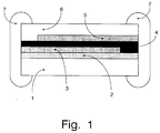
- 1 denotes a substrate layer, for example glass or Al 2 O 3 , 2 an anti-reaction or planarization layer, 3 a first electrode, 4 a dielectric layer, 5 a second electrode, 6 a protective layer and 7 two on both sides attached end contacts.
- a substrate layer for example glass or Al 2 O 3
- 2 an anti-reaction or planarization layer
- 3 a first electrode
- 4 a dielectric layer
- 5 a second electrode
- 6 a protective layer
- 7 two on both sides attached end contacts.
- other embodiments are also conceivable.
- a thin Ti layer 2 is applied to a glass substrate 1 (Corning 7059) by a sputtering process and then oxidized.
- a Ti / Pt layer 3 is then sputtered on.
- this electrode layer is sputtered through a mechanical mask.
- a PbZr 0.35 Ti 0.65 O 3 layer 4 is applied to this substrate.
- the PbZr 0.35 Ti 0.65 O 3 layer 4 is deposited by using a solution in which lead acetate trihydrate was dissolved in 60 g of ethylene glycol monomethyl ether. 8.62 g of titanium tetra-n-butoxide and 7.51 g of zirconium tetra-n-butoxide were added to this solution.
- the solution was filtered through a cellulose acetate filter with a pore size of 0.2 ⁇ m.
- a glass substrate 1 with a structured Pt electrode 3 is used to deposit a PZT layer 4.
- Approx. 1 ml of the Pb-Ti-Zr solution is applied to this substrate and thus coated with a centrifugal process at 2500 revolutions per minute.
- the layer is heated at 100 ° C./sec to 550 ° C. under an oxygen atmosphere and then sintered at this temperature. This process is repeated several times in order to produce a layer with a layer thickness of approximately 0.3-1 ⁇ m.
- a second Pt electrode 5 is sputtered onto this PZT layer 4 through a mechanical mask. After depositing a 0.5 ⁇ m thick SiO 2 layer and an organic protective layer 6, the substrates are divided into strips and then provided with end contacts 7.
- a thin Ti layer 2 is applied to a glass substrate 1 (Schott AF45) by a sputtering process and thermally oxidized. Then a Ti / Pt layer 3 is sputtered on. For structuring, this electrode is treated by reactive ion etching.
- a PbZr 0.35 Ti 0.65 O 3 layer 4 is applied to this substrate.
- a PbZr 0.35 Ti 0.65 O 3 layer 4 is deposited by using a solution in which lead acetate trihydrate has been dissolved in 60 g of ethylene glycol monomethyl ether. 8.62 g of titanium tetra-n-butoxide and 7.51 g of zirconium tetra-n-butoxide were added to this solution.
- the solution was filtered through a cellulose acetate filter with a pore size of 0.2 ⁇ m.
- the glass substrate 1 with structured Pt electrode 3 is used to deposit a PZT layer 4.
- Approx. 1 ml of the Pb-Ti-Zr solution is applied to this substrate and coated with a centrifugal process at 2500 revolutions per minute.
- the layer is heated at 100 ° C./sec to 550 ° C. under an oxygen atmosphere and then sintered at this temperature. This process is repeated several times to produce a layer of approximately 0.2-1 ⁇ m.
- a Pt electrode 5 is sputtered onto this PZT layer 4 and structured by reactive ion etching.
- the further processing to form a capacitor component takes place in accordance with exemplary embodiment 1.
- a thin Ti and Ti / Pt layer 2 and 3 is sputtered and structured in accordance with embodiment 2 by a sputtering process.
- a PbZr 0.35 Ti 0.65 O 3 layer 4 is applied to this substrate.
- a PbZr 0.35 Ti 0.65 O 3 layer 4 is deposited by using a solution in which lead acetate trihydrate has been dissolved in 60 g of ethylene glycol monomethyl ether. 8.62 g of titanium tetra-n-butoxide and 7.51 g of zirconium tetra-n-butoxide were added to this solution. The solution was filtered through a cellulose acetate filter with a pore size of 0.2 ⁇ m.
- the glass substrate 1 with structured Pt electrode 3 is used to deposit a PZT layer 4. Approx. 1 ml of the Pb-Ti-Zr solution is applied to this substrate and coated with a centrifugal process at 2500 revolutions per minute. The layer is heated at 300 ° C./min to 600 ° C. under an oxygen atmosphere and then sintered at this temperature.
- a second layer of the composition PbZr 0.53 Ti 0.47 O 3 is applied to this layer.
- lead acetate is dissolved in methoxyethanol.
- 4.204 g of titanium tetra-n-butoxide and 5.076 g of zirconium tetra-n-butoxide are dissolved in methoxyethanol.
- the solution containing titanium and zirconium is added to the lead acetate solution with stirring.
- a hydrolyzing solution of water and conc. HNO 3 and methoxyethanol produced. This hydrolyzing solution is added to the solution containing lead, titanium and zircon.
- a thin Ti / Pt layer 2 and 3 with 10 nm Ti and 140 nm Pt is sputtered onto a glass substrate 1 (corresponding to embodiment 1, 2 or 3).
- the continuous Pt electrode 3 is structured by a reactive ion etching process.
- An anti-reaction layer 2 consisting of TiO 2 is then produced on the substrate 1 by converting the continuous Ti layer into a dense TiO 2 layer 2 by means of a thermal treatment at 450 ° C. in an oxygen stream.
- a PbZr 0.35 T 0.65 O 3 layer and a PbZr 0.53 Ti 0.47 O 3 layer 4, which is doped with La, are applied to this substrate.
- a Pb-La-Ti-Zr solution is produced in a manner similar to that of the solutions described in working examples 1, 2, 3.
- the glass substrate 1, as provided above with an anti-reaction layer 2, is used.
- the layer structures are deposited as in exemplary embodiment 3.
- a Pt layer is applied to this PZT layer 4 by a sputtering process.
- This upper electrode 5 is structured by reactive ion etching.
- a protective layer 6 consisting of 0.5 ⁇ m SiO 2 is then applied and structured by chemical deposition.
- a 10 ⁇ m thick polymer layer in the form of polyimide is applied and structured on the SiO 2 layer.
- the glass substrate is separated into strips.
- NiCr end contacts 7 are sputtered on and NiPbSn end contacts 7 are in grew up in a galvanic bath.
- End contacts are printed on a glass substrate 1 (Schott AF45) by a printing process on the underside of the substrate.
- a thin ZrO 2 layer is then applied as an anti-reaction layer 2 to the glass substrate by means of a centrifugal process.
- a thin Ti / Pt layer 2 and 3 with 10 nm Ti and 140 nm Pt is applied in a structured manner to this anti-reaction layer 2 by means of the lift-off method.
- a layer structure 4 composed of a PbZr 0.35 Ti 0.65 O 3 layer and a PbZr 0.53 Ti 0.47 O 3 layer, which is doped with La, is applied to this substrate. The coating is carried out as described in Example 4.
- a Pt layer 5 is applied to the PLZT layer 4.
- This upper electrode 5 is structured by a lift-off method.
- a protective layer 6 consisting of 0.5 ⁇ m Si 3 N 4 is then deposited by means of PECVD. After structuring the Si 3 N 4 layer, an approximately 10 ⁇ m thick polyimide layer is applied and structured. After separation into strips, NiCr end contacts 7 are sputtered on. After the complete separation into individual products, NiPbSn end contacts 7 are grown in a galvanic bath.
- End contacts are printed on an Al 2 O 3 substrate 1 (thick-film quality) by a printing process on the underside of the substrate.
- a lead silicate layer is then printed on as planarization layer 2 by a further printing process.
- a lead silicate powder is dispersed in isopropanol. Coarse particles are removed by sedimentation. The remaining slurry is applied to the Al 2 O 3 substrate 1 by means of a doctor blade process. The substrate is dried and then sintered at 900 ° C.
- a thin Ti / Pt layer 2 and 3 with 10 nm Ti and 140 nm Pt is sputtered and structured onto this planarized substrate 1 and 2 using the lift-off method.
- a Pt layer 5 is applied to the PLZT layer 4.
- This upper electrode 5 is structured by a printing process and a lift-off process.
- a low-sintering glass layer is then printed on as a protective layer 6.
- NiCr end contacts 7 are sputtered on.
- NiPbSn end contacts 7 are grown in a galvanic bath.
Landscapes
- Chemical & Material Sciences (AREA)
- Engineering & Computer Science (AREA)
- Materials Engineering (AREA)
- Power Engineering (AREA)
- Chemical Kinetics & Catalysis (AREA)
- General Chemical & Material Sciences (AREA)
- Geochemistry & Mineralogy (AREA)
- Organic Chemistry (AREA)
- Life Sciences & Earth Sciences (AREA)
- Microelectronics & Electronic Packaging (AREA)
- Manufacturing & Machinery (AREA)
- Ceramic Engineering (AREA)
- Inorganic Chemistry (AREA)
- Fixed Capacitors And Capacitor Manufacturing Machines (AREA)
- Ceramic Capacitors (AREA)
- Compositions Of Oxide Ceramics (AREA)
- Inorganic Insulating Materials (AREA)
Abstract
Description
TiO2, ZrO2, HfO2, SrTiO3, CaTiO3, CaZrO3, BaTiO3, BaZrxTi1-xO3 mit x=0..1,PbZrxTi1-xO3 mit x=0..1, Ta2O5, Nb2O5, MgO, BeO, Al2O3, MgAl2O4, ZrTiO4, BaF2, MgF2,Y2O3, Sc2O3, La2O3 und Ln2O3, wobei Ln Lanthanide wie z.B. Pr2O3 sind, vorgesehen sind. Ähnlich wie bei einem erfindungsgemäßen Kondensator mit einem Glassubstrat und einer Antireaktionsschicht werden dielektrische Materialien eingesetzt, die Dielektrizitätskonstanten K>10 haben, um hohe Kapazitäten in kleinen Abmessungen zu erreichen. Um diese Materialien auf einem kostengünstigen Al2O3-Substrat verwenden zu können, muß eine Planarisierungsschicht vorgesehen werden, da neben einer Reaktion des Dielektrikums mit Al2O3 auch Kurzschlüsse der Kondensatoren aufgrund der hohen Oberflächenrauhigkeit verhindert werden müssen. Weiterhin wird auch eine Rißbildung der dielektrischen Schicht durch unterschiedliche thermische Ausdehnungskoeffizienten vermieden. Bei einer Planarisierungsschicht aus einem der oben angegebenen Stoffe oder einer Kombination aus mehreren Stoffen auf dem Al2O3-Substrat kann darauf eine dielektrische Schicht aufgebracht werden, mit der eine ausreichende Kapazität erreicht wird. Im Falle von sehr oberflächenrauhen Substraten, wie z.B. Al2O3 - Substraten mit Dickschichtqualität, werden mehrere Mikrometer dicke Planarisierungsschichten aufgebracht. Diese Planarisierungsschicht kann z.B. eine Blei-Silikatglasschicht oder auch zur Erhöhung der Temperaturstabilität eine mit TiO2, ZrO2 oder auch PbTiO3 oder einem der anderen oben angegebenen Zusätze angereicherte Glasschicht sein. Als Verfahren zur Abscheidung einiger Mikrometer dicker Schichten können hier z.B. Dickschichtprozesse, wie z.B. Siebdruckprozesse, eingesetzt werden.
PbTiO3 und Pb(Mg1/3Nb2/3)O3+Flüssigphase
- Bereitstellen wenigstens einer Substratschicht aus Glas,
- Aufbringen wenigstens einer Antireaktionsschicht auf die Substratschicht,
- Aufbringen wenigstens einer ersten Elektrodenschicht auf die Antireaktionsschicht,
- Strukturierung der ersten Elektrodenschicht zu wenigstens einer ersten Elektrode,
- Aufbringen wenigstens einer Dielektrikumschicht auf die erste Elektrode,
- Aufbringen wenigstens einer zweiten Elektrodenschicht auf die Dielektrikumschicht,
- Strukturierung der zweiten Elektrodenschicht zu wenigstens einer zweiten Elektrode
- Bereitstellen wenigstens einer Substratschicht aus Al2O3,
- Aufbringen wenigstens einer Planarisierungsschicht auf die Substratschicht,
- Aufbringen wenigstens einer ersten Elektrodenschicht auf die Planarisierungsschicht,
- Strukturierung der ersten Elektrodenschicht zu wenigstens einer ersten Elektrode,
- Aufbringen wenigstens einer Dielektrikumschicht auf die erste Elektrode,
- Aufbringen wenigstens einer zweiten Elektrodenschicht auf die Dielektrikumschicht,
- Strukturierung der zweiten Elektrodenschicht zu wenigstens einer zweiten Elektrode
- Fig. 1:
- den schematischen Aufbau des erfindungsgemäßen Bauteiles im Querschnitt.
Claims (14)
- Bauteil mit einem Kondensator mitdadurch gekennzeichnet,wenigstens einer Substratschicht (1) aus Glas,wenigstens einer Antireaktionsschicht (2),wenigstens zwei Elektrodenschichten (3, 5) undwenigstens einer Dielektrikumschicht (4),
daß als Material für die Antireaktionsschicht (2) wenigstens ein Element aus einer Gruppe, bestehend aus TiO2, ZrO2, HfO2, SrTiO3, CaTiO3, BaTiO3, BaZrxTi1-xO3 mit x=0..1, PbZrxTi1-xO3 mit x=0..1, Ta2O5, Nb2O5, MgO, BeO, Al2O3, MgAl2O4, ZrTiO4, BaF2, TiB2, MgF2, Y2O3, Sc2O3, La2O3 und Ln2O3, wobei Ln Lanthanide wie z.B. Pr2O3 sind, vorgesehen ist. - Bauteil nach Anspruch 1,
dadurch gekennzeichnet,
daß als Material für die Elelctrodenschichten (3, 5) jeweils wenigstens ein Element aus einer Gruppe, bestehend aus Ti/Pt, Ta/Pt, Ti/Pd/Pt, Ir, IrOx, IrO2/Ir, ZrO2/Pt, Ti/Cu, Ti/Ni, Ti/NiAl, Ti/(Ni, Al, Cr), Ti/(Ni, Al, Fe), Ti/(Ni, Fe, Cr), Ti/(Ni, Al, Cr, Fe), Ti/(Ni, Fe, Cr, Si), Ti/(Co, Ni, Fe, Cr), PtxAl1-x/Pt, Pt/IrO2, TiO2/Pt, leitenden Oxiden, Hybriden aus wenigstens einem leitenden Oxid und einem Edelmetall und Hybriden aus wenigstens einem Edelmetall und einem Nichtedelmetall, vorgesehen ist. - Bauteil nach Anspruch 1 oder 2,
dadurch gekennzeichnet,
daß für die Dielektrikumschicht (4) eine Schicht aus ferroelektrischem Material mit einer Dicke von 10 nm bis 2 µm vorgesehen ist. - Bauteil mit einem Kondensator mitdadurch gekennzeichnet,wenigstens einer Substratschicht (1) aus Al2O3,wenigstens einer Planarisierungsschicht (2),wenigstens zwei Elektrodenschichten (3, 5) undwenigstens einer Dielektrikumschicht (4),
daß als Material für die Planarisierungsschicht (2) nicht kristallisierende Gläser mit/ohne Zusatz von wenigstens einem Element aus einer Gruppe, bestehend aus TiO2, ZrO2, HfO2, SrTiO3, CaTiO3, CaZrO3, BaTiO3, BaZrxTi1-xO3 mit x=0..1,PbZrxTi1-xO3 mit x=0..1, Ta2O5, Nb2O5, MgO, BeO, Al2O3, MgAl2O4, ZrTiO4, BaF2, MgF2,Y2O3, Sc2O3, La2O3 und Ln2O3, wobei Ln Lanthanide wie z.B. Pr2O3 sind, vorgesehen sind. - Bauteil nach Anspruch 4,
dadurch gekennzeichnet,
daß als Material für die Elektrodenschichten (3, 5) jeweils wenigstens ein Element aus einer Gruppe, bestehend aus Ti/Pt, Ta/Pt, Ti/Pd/Pt, Ir, IrOx, IrO2/Ir, ZrO2/Pt, Ti/Cu, Ti/Ni, Ti/NiAl, Ti/(Ni, Al, Cr), Ti/(Ni, Al, Fe), Ti/(Ni, Fe, Cr), Ti/(Ni, Al, Cr, Fe), Ti/(Ni, Fe, Cr, Si), Ti/(Co, Ni, Fe, Cr), PtxAl1-x/Pt, Pt/IrO2, TiO2/Pt, leitenden Oxiden, Hybriden aus wenigstens einem leitenden Oxid und einem Edelmetall und Hybriden aus wenigstens einem Edelmetall und einem Nichtedelmetall, vorgesehen ist. - Bauteil nach Anspruch 4 oder 5,
dadurch gekennzeichnet,
daß für die Dielektrikumschicht (4) eine Schicht aus ferroelektrischem Material mit einer Dicke von 10 nm bis 2 µm vorgesehen ist. - Bauteil nach Anspruch 4,
dadurch gekennzeichnet,
daß als Material für die Elektrodenschichten (3, 5) jeweils Wenigstens ein Metallpulver in Form einer Paste aus einer Gruppe, bestehend aus AgxPt1-x mit x=0..1, AgxPd1-x mit x=0..1, Ag, Cu, Ni und diese Metallpulver jeweils mit Zugabe geringer Mengen eines Haftglases, vorgesehen ist. - Bauteil nach Anspruch 4 oder 7,
dadurch gekennzeichnet,
daß für die Dielektrikumschicht (4) eine Schicht aus ferroelektrischem Material mit einer Dicke von 2 µm bis 20 µm vorgesehen ist. - Bauteil nach einem der Ansprüche 1 bis 8,
dadurch gekennzeichnet,
daß wenigstens eine organische oder anorganische Schutzschicht (6) vorgesehen ist. - Bauteil nach einem der Ansprüche 1 bis 9,
dadurch gekennzeichnet,
daß wenigstens zwei Endkontakte (7) vorgesehen sind. - Kondensator mitdadurch gekennzeichnet,wenigstens einer Substratschicht (1) aus Glas,wenigstens einer Antireaktionsschicht (2),wenigstens zwei Elektrodenschichten (3, 5) undwenigstens einer Dielektrikumschicht (4),
daß als Material für die Antireaktionsschicht (2) wenigstens ein Element aus einer Gruppe, bestehend aus TiO2, ZrO2, HfO2, SrTiO3, CaTiO3, BaTiO3, BaZrxTi1-xO3 mit x=0..1, PbZrxTi1-xO3 mit x=0..1, Ta2O5, Nb2O5, MgO, BeO, Al2O3, MgAl2O4, ZrTiO4, BaF2, TiB2,MgF2, Y2O3, Sc2O3, La2O3 und Ln2O3, wobei Ln Lanthanide wie z.B. Pr2O3 sind, vorgesehen ist. - Kondensator mitdadurch gekennzeichnet,wenigstens einer Substratschicht (1) aus Al2O3,wenigstens einer Planarisierungsschicht (2),wenigstens zwei Elektrodenschichten (3, 5) undwenigstens einer Dielektrikumschicht (4),
daß als Material für die Planarisierungsschicht (2) nicht kristallisierende Gläser mit/ohne Zusatz von wenigstens einem Element aus einer Gruppe, bestehend aus TiO2, ZrO2, HfO2, SrTiO3, CaTiO3, CaZrO3, BaTiO3, BaZrxTi1-xO3 mit x=0..1,PbZrxTi1-xO3 mit x=0..1, Ta2O5, Nb2O5, MgO, BeO, Al2O3, MgAl2O4, ZrTiO4, BaF2, MgF2,Y2O3, Sc2O3, La2O3 und Ln2O3, wobei Ln Lanthanide wie z.B. Pr2O3 sind, vorgesehen sind. - Verfahren zur Herstellung eines Bauteiles mit einem Kondensator mit den Schrittendadurch gekennzeichnet,Bereitstellen wenigstens einer Substratschicht (1) aus Glas,Aufbringen wenigstens einer Antireaktionsschicht (2) auf die Substratschicht (1),Aufbringen wenigstens einer ersten Elektrodenschicht (3) auf die Antireaktionsschicht (2),Strukturierung der ersten Elektrodenschicht (3) zu wenigstens einer ersten Elektrode (3),Aufbringen wenigstens einer Dielektrikumschicht (4) auf die erste Elektrode (3),Aufbringen wenigstens einer zweiten Elektrodenschicht (5) auf die Dielektrikumschicht (4),Strukturierung der zweiten Elektrodenschicht (5) zu wenigstens einer zweiten Elektrode (5),
daß als Material für die Antireaktionsschicht (2) wenigstens ein Element aus einer Gruppe, bestehend aus TiO2, ZrO2, HfO2, SrTiO3, CaTiO3, BaTiO3, BaZrxTi1-xO3 mit x=0..1, PbZrxTi1-xO3 mit x=0..1, Ta2O5, Nb2O5, MgO, BeO, Al2O3, MgAl2O4,ZrTiO4, BaF2, MgF2, Y2O3, Sc2O3, La2O3 und Ln2O3, wobei Ln Lanthanide wie z.B. Pr2O3 sind, vorgesehen ist. - Verfahren zur Herstellung eines Bauteiles mit einem Kondensator mit den Schrittendadurch gekennzeichnet,Bereitstellen wenigstens einer Substratschicht (1) aus Al2O3,Aufbringen wenigstens einer Planarisierungsschicht (2) auf die Substratschicht (1),Aufbringen wenigstens einer ersten Elektrodenschicht (3) auf die Planarisierungsschicht (2),Strukturierung der ersten Elektrodenschicht (3) zu wenigstens einer ersten Elektrode (3),Aufbringen wenigstens einer Dielektrikumschicht (4) auf die erste Elektrode (3),Aufbringen wenigstens einer zweiten Elektrodenschicht (5) auf die Dielektrikumschicht (4),Strukturierung der zweiten Elektrodenschicht (5) zu wenigstens einer zweiten Elektrode (5),
daß als Material für die Planarisierungsschicht (2) nicht kristallisierende Gläser mit/ohne Zusatz von wenigstens einem Element aus einer Gruppe, bestehend aus TiO2, ZrO2, HfO2, SrTiO3, CaTiO3, BaTiO3, BaZrxTi1-xO3 mit x=0..1, PbZrxTi1-xO3 mit x=0..1, Ta2O5, Nb2O5, MgO, BeO, Al2O3, MgAl2O4, ZrTiO4, BaF2, MgF2,Y2O3, Sc2O3, La2O3 und Ln2O3, wobei Ln Lanthanide wie z.B. Pr2O3 sind, vorgesehen sind.
Applications Claiming Priority (2)
| Application Number | Priority Date | Filing Date | Title |
|---|---|---|---|
| DE19630883A DE19630883A1 (de) | 1996-07-31 | 1996-07-31 | Bauteil mit einem Kondensator |
| DE19630883 | 1996-07-31 |
Publications (3)
| Publication Number | Publication Date |
|---|---|
| EP0823718A2 true EP0823718A2 (de) | 1998-02-11 |
| EP0823718A3 EP0823718A3 (de) | 1999-12-29 |
| EP0823718B1 EP0823718B1 (de) | 2006-12-06 |
Family
ID=7801368
Family Applications (1)
| Application Number | Title | Priority Date | Filing Date |
|---|---|---|---|
| EP97202076A Expired - Lifetime EP0823718B1 (de) | 1996-07-31 | 1997-07-04 | Bauteil mit einem Kondensator |
Country Status (4)
| Country | Link |
|---|---|
| US (1) | US6125027A (de) |
| EP (1) | EP0823718B1 (de) |
| JP (1) | JPH1083934A (de) |
| DE (2) | DE19630883A1 (de) |
Cited By (3)
| Publication number | Priority date | Publication date | Assignee | Title |
|---|---|---|---|---|
| EP0960868A1 (de) * | 1998-05-27 | 1999-12-01 | Koninklijke Philips Electronics N.V. | Dielektrische keramische Zusammensetzung |
| EP1022768A2 (de) * | 1999-01-20 | 2000-07-26 | Philips Corporate Intellectual Property GmbH | Spannungsfester Dünnschichtkondensator mit Interdigitalstruktur |
| EP1067685A3 (de) * | 1999-07-07 | 2001-06-27 | Philips Corporate Intellectual Property GmbH | Volumenwellen-Filter |
Families Citing this family (24)
| Publication number | Priority date | Publication date | Assignee | Title |
|---|---|---|---|---|
| EP0996958A2 (de) * | 1998-04-20 | 2000-05-03 | Koninklijke Philips Electronics N.V. | Dünnfilmkondensator |
| EP1048042A1 (de) * | 1998-09-02 | 2000-11-02 | Koninklijke Philips Electronics N.V. | Dünnfilmkondensator |
| JP3423232B2 (ja) * | 1998-11-30 | 2003-07-07 | 三洋電機株式会社 | アクティブ型el表示装置 |
| WO2001054200A1 (en) | 2000-01-19 | 2001-07-26 | North Carolina State University | Lanthanum oxide-based gate dielectrics for integrated circuit field effect transistors and methods of fabricating same |
| US6400072B1 (en) * | 2000-03-08 | 2002-06-04 | Motorola, Inc. | Viewing screen for a display device |
| US6411492B1 (en) * | 2000-05-24 | 2002-06-25 | Conexant Systems, Inc. | Structure and method for fabrication of an improved capacitor |
| WO2002017430A1 (en) * | 2000-08-22 | 2002-02-28 | Paratek Microwave, Inc. | Combline filters with tunable dielectric capacitors |
| US6985349B2 (en) * | 2001-12-13 | 2006-01-10 | Harris Corporation | Electronic module including a low temperature co-fired ceramic (LTCC) substrate with a capacitive structure embedded therein and related methods |
| JP4218350B2 (ja) * | 2002-02-01 | 2009-02-04 | パナソニック株式会社 | 強誘電体薄膜素子およびその製造方法、これを用いた薄膜コンデンサ並びに圧電アクチュエータ |
| US6917509B1 (en) * | 2002-11-21 | 2005-07-12 | Daniel F. Devoe | Single layer capacitor with dissimilar metallizations |
| US6716692B1 (en) * | 2003-05-20 | 2004-04-06 | Via Technologies, Inc. | Fabrication process and structure of laminated capacitor |
| US7290315B2 (en) * | 2004-10-21 | 2007-11-06 | Intel Corporation | Method for making a passive device structure |
| US7375412B1 (en) * | 2005-03-31 | 2008-05-20 | Intel Corporation | iTFC with optimized C(T) |
| US20060220177A1 (en) * | 2005-03-31 | 2006-10-05 | Palanduz Cengiz A | Reduced porosity high-k thin film mixed grains for thin film capacitor applications |
| US7629269B2 (en) * | 2005-03-31 | 2009-12-08 | Intel Corporation | High-k thin film grain size control |
| US7453144B2 (en) * | 2005-06-29 | 2008-11-18 | Intel Corporation | Thin film capacitors and methods of making the same |
| JP5910317B2 (ja) * | 2012-05-28 | 2016-04-27 | Tdk株式会社 | 誘電体磁器組成物および電子部品 |
| JP5772808B2 (ja) * | 2012-12-25 | 2015-09-02 | 株式会社村田製作所 | 積層セラミック電子部品 |
| US9370103B2 (en) * | 2013-09-06 | 2016-06-14 | Qualcomm Incorported | Low package parasitic inductance using a thru-substrate interposer |
| CN104628378B (zh) * | 2015-02-05 | 2017-02-22 | 汕头高新区松田实业有限公司 | 一种可用于铜电极陶瓷电容器的介质及其制备方法 |
| EP3417540B1 (de) * | 2016-04-12 | 2021-11-10 | Siemens Energy Global GmbH & Co. KG | Elektrischer kondensator |
| CN109087674A (zh) * | 2017-06-14 | 2018-12-25 | 萨摩亚商费洛储存科技股份有限公司 | 铁电内存及其数据读取、写入与制造方法和电容结构 |
| US11037728B2 (en) | 2017-12-22 | 2021-06-15 | Samsung Electronics Co., Ltd. | Dielectric and capacitor and electronic device |
| CN112661509B (zh) * | 2020-12-24 | 2022-08-02 | 电子科技大学 | 一种高Q值MgZrNb2O8基微波介质陶瓷材料及其制备方法 |
Citations (1)
| Publication number | Priority date | Publication date | Assignee | Title |
|---|---|---|---|---|
| DE3414808A1 (de) * | 1983-06-17 | 1984-12-20 | AVX Corp.,(n.d.Ges.d.Staates Delaware), Great Neck, N.Y. | Verfahren zur herstellung eines preiswerten duennfilmkondensators und danach hergestellter kondensator |
Family Cites Families (26)
| Publication number | Priority date | Publication date | Assignee | Title |
|---|---|---|---|---|
| US3566204A (en) * | 1969-04-04 | 1971-02-23 | Mallory & Co Inc P R | Ceramic chip capacitor having coplanar surfaces |
| JPS56140614A (en) * | 1980-04-03 | 1981-11-04 | Murata Manufacturing Co | Capacitor and method of manufacturing same |
| US4654095A (en) * | 1985-03-25 | 1987-03-31 | E. I. Du Pont De Nemours And Company | Dielectric composition |
| US4772985A (en) * | 1986-09-24 | 1988-09-20 | Kabushiki Kaisha Toshiba | Thick film capacitor |
| US4766027A (en) * | 1987-01-13 | 1988-08-23 | E. I. Du Pont De Nemours And Company | Method for making a ceramic multilayer structure having internal copper conductors |
| US4855266A (en) * | 1987-01-13 | 1989-08-08 | E. I. Du Pont De Nemours And Company | High K dielectric composition for use in multilayer ceramic capacitors having copper internal electrodes |
| US4835656A (en) * | 1987-04-04 | 1989-05-30 | Mitsubishi Mining And Cement Co., Ltd. | Multi-layered ceramic capacitor |
| JPH0648666B2 (ja) * | 1987-09-29 | 1994-06-22 | 三菱マテリアル株式会社 | 積層セラミックコンデンサ及びその製法 |
| US5046043A (en) * | 1987-10-08 | 1991-09-03 | National Semiconductor Corporation | Ferroelectric capacitor and memory cell including barrier and isolation layers |
| US5258335A (en) * | 1988-10-14 | 1993-11-02 | Ferro Corporation | Low dielectric, low temperature fired glass ceramics |
| US5005102A (en) * | 1989-06-20 | 1991-04-02 | Ramtron Corporation | Multilayer electrodes for integrated circuit capacitors |
| FI84869C (fi) * | 1990-06-11 | 1992-01-27 | Planar Int Oy | Matrisfilmstruktur i synnerhet foer elektroluminecens displayenhet. |
| WO1992019564A1 (en) * | 1991-05-01 | 1992-11-12 | The Regents Of The University Of California | Amorphous ferroelectric materials |
| US5723361A (en) * | 1991-12-13 | 1998-03-03 | Symetrix Corporation | Thin films of ABO3 with excess A-site and B-site modifiers and method of fabricating integrated circuits with same |
| US5624707A (en) * | 1991-12-13 | 1997-04-29 | Symetrix Corporation | Method of forming ABO3 films with excess B-site modifiers |
| JPH05326315A (ja) * | 1992-05-25 | 1993-12-10 | Itochu Fine Chem Kk | 薄膜コンデンサおよびその製造装置 |
| JPH0714993A (ja) * | 1993-06-18 | 1995-01-17 | Mitsubishi Electric Corp | 半導体装置およびその製造方法 |
| US5489548A (en) * | 1994-08-01 | 1996-02-06 | Texas Instruments Incorporated | Method of forming high-dielectric-constant material electrodes comprising sidewall spacers |
| US5504041A (en) * | 1994-08-01 | 1996-04-02 | Texas Instruments Incorporated | Conductive exotic-nitride barrier layer for high-dielectric-constant materials |
| US6331325B1 (en) * | 1994-09-30 | 2001-12-18 | Texas Instruments Incorporated | Barium strontium titanate (BST) thin films using boron |
| US5822175A (en) * | 1995-04-13 | 1998-10-13 | Matsushita Electronics Corporation | Encapsulated capacitor structure having a dielectric interlayer |
| US5612560A (en) * | 1995-10-31 | 1997-03-18 | Northern Telecom Limited | Electrode structure for ferroelectric capacitors for integrated circuits |
| JPH09298127A (ja) * | 1996-05-09 | 1997-11-18 | Murata Mfg Co Ltd | 積層コンデンサ |
| JP3180681B2 (ja) * | 1996-07-19 | 2001-06-25 | 株式会社村田製作所 | 積層セラミックコンデンサ |
| JPH113834A (ja) * | 1996-07-25 | 1999-01-06 | Murata Mfg Co Ltd | 積層セラミックコンデンサおよびその製造方法 |
| US5790366A (en) * | 1996-12-06 | 1998-08-04 | Sharp Kabushiki Kaisha | High temperature electrode-barriers for ferroelectric and other capacitor structures |
-
1996
- 1996-07-31 DE DE19630883A patent/DE19630883A1/de not_active Withdrawn
-
1997
- 1997-07-04 DE DE59712775T patent/DE59712775D1/de not_active Expired - Fee Related
- 1997-07-04 EP EP97202076A patent/EP0823718B1/de not_active Expired - Lifetime
- 1997-07-30 US US08/903,143 patent/US6125027A/en not_active Expired - Lifetime
- 1997-07-30 JP JP9204686A patent/JPH1083934A/ja active Pending
Patent Citations (1)
| Publication number | Priority date | Publication date | Assignee | Title |
|---|---|---|---|---|
| DE3414808A1 (de) * | 1983-06-17 | 1984-12-20 | AVX Corp.,(n.d.Ges.d.Staates Delaware), Great Neck, N.Y. | Verfahren zur herstellung eines preiswerten duennfilmkondensators und danach hergestellter kondensator |
Cited By (5)
| Publication number | Priority date | Publication date | Assignee | Title |
|---|---|---|---|---|
| EP0960868A1 (de) * | 1998-05-27 | 1999-12-01 | Koninklijke Philips Electronics N.V. | Dielektrische keramische Zusammensetzung |
| EP1022768A2 (de) * | 1999-01-20 | 2000-07-26 | Philips Corporate Intellectual Property GmbH | Spannungsfester Dünnschichtkondensator mit Interdigitalstruktur |
| EP1022768A3 (de) * | 1999-01-20 | 2004-05-06 | Philips Intellectual Property & Standards GmbH | Spannungsfester Dünnschichtkondensator mit Interdigitalstruktur |
| EP1067685A3 (de) * | 1999-07-07 | 2001-06-27 | Philips Corporate Intellectual Property GmbH | Volumenwellen-Filter |
| US6466105B1 (en) | 1999-07-07 | 2002-10-15 | Koninklijke Philips Electronics N.V. | Bulk acoustic wave filter |
Also Published As
| Publication number | Publication date |
|---|---|
| EP0823718A3 (de) | 1999-12-29 |
| EP0823718B1 (de) | 2006-12-06 |
| DE59712775D1 (de) | 2007-01-18 |
| DE19630883A1 (de) | 1998-02-05 |
| US6125027A (en) | 2000-09-26 |
| JPH1083934A (ja) | 1998-03-31 |
Similar Documents
| Publication | Publication Date | Title |
|---|---|---|
| EP0823718B1 (de) | Bauteil mit einem Kondensator | |
| EP0459575B1 (de) | Verfahren zur Herstellung von Monolayer-Kondensatoren | |
| DE69710259T2 (de) | Dielektrische keramische Zusammensetzung und ihre Verwendung in einem monolithischen keramischen Kondensator | |
| DE69034034T2 (de) | Keramischer Mehrschicht-Chipkondensator und Verfahren zu seiner Herstellung | |
| DE69710265T2 (de) | Dielektrische keramische Zusammensetzung und diese verwendender monolithischer keramischer Kondensator | |
| DE69609119T2 (de) | Dielektrische keramische Zusammensetzungen | |
| DE69807366T2 (de) | Monolithischer keramischer Kondensator | |
| DE69928873T2 (de) | Dielektrische keramische Zusammensetzung und keramischer Vielschichtkondensator | |
| DE69516045T2 (de) | Keramischer Mehrschichtkondensator und Herstellungsverfahren | |
| DE69720168T2 (de) | Keramische Zusammensetzung und diese verwendender keramischer Kondensator | |
| DE4421007A1 (de) | Elektronisches Bauteil und Verfahren zu seiner Herstellung | |
| DE69604510T2 (de) | Monolithische keramische Kondensatoren | |
| DE69822933T2 (de) | Dielektrische keramische Zusammensetzung und deren Verwendung in einem monolithischen keramischen Kondensator | |
| DE69700235T2 (de) | Monolithischer keramischer Kondensator | |
| EP0782156A2 (de) | Vielschichtkondensator mit Dielektrikum aus modifiziertem Bariumstrontiumtitanat | |
| EP1022768A2 (de) | Spannungsfester Dünnschichtkondensator mit Interdigitalstruktur | |
| EP1145261A1 (de) | Kondensator mit bczt-dielektrikum | |
| DE4005505A1 (de) | Monolithischer keramischer kondensator | |
| DE10040414B4 (de) | Dielelektrisches Keramikmaterial und elektrisches Bauelement | |
| EP1263691B1 (de) | Keramikmasse, verfahren zur herstellung der keramikmasse und verwendung der keramikmasse | |
| EP0676384B1 (de) | Perowskithaltiger Verbundwerkstoff, Verfahren zu seiner Herstellung, elektronisches Bauelement und Modul | |
| DE60126700T2 (de) | Verfahren zur Herstellung einer keramischen Zusammensetzung und Verfahren zur Herstellung eines elektronischen Geräts | |
| DE69021809T2 (de) | Verfahren zur herstellung keramischer kondensatoren mit varistor-kennzeichen. | |
| EP0914677A1 (de) | Schichtaufbau mit einer ferroelektrischen schicht und herstellverfahren | |
| DE19653792A1 (de) | Bauteil mit flacher Temperaturcharakteristik |
Legal Events
| Date | Code | Title | Description |
|---|---|---|---|
| PUAI | Public reference made under article 153(3) epc to a published international application that has entered the european phase |
Free format text: ORIGINAL CODE: 0009012 |
|
| AK | Designated contracting states |
Kind code of ref document: A2 Designated state(s): DE FR GB |
|
| AX | Request for extension of the european patent |
Free format text: AL;LT;LV;RO;SI |
|
| RAP3 | Party data changed (applicant data changed or rights of an application transferred) |
Owner name: KONINKLIJKE PHILIPS ELECTRONICS N.V. Owner name: PHILIPS PATENTVERWALTUNG GMBH |
|
| PUAL | Search report despatched |
Free format text: ORIGINAL CODE: 0009013 |
|
| AK | Designated contracting states |
Kind code of ref document: A3 Designated state(s): AT BE CH DE DK ES FI FR GB GR IE IT LI LU MC NL PT SE |
|
| AX | Request for extension of the european patent |
Free format text: AL;LT;LV;RO;SI |
|
| RIC1 | Information provided on ipc code assigned before grant |
Free format text: 6H 01G 4/12 A, 6H 01G 7/06 B |
|
| RAP3 | Party data changed (applicant data changed or rights of an application transferred) |
Owner name: KONINKLIJKE PHILIPS ELECTRONICS N.V. Owner name: PHILIPS CORPORATE INTELLECTUAL PROPERTY GMBH |
|
| 17P | Request for examination filed |
Effective date: 20000629 |
|
| AKX | Designation fees paid |
Free format text: DE FR GB |
|
| RAP1 | Party data changed (applicant data changed or rights of an application transferred) |
Owner name: KONINKLIJKE PHILIPS ELECTRONICS N.V. Owner name: PHILIPS CORPORATE INTELLECTUAL PROPERTY GMBH |
|
| RAP1 | Party data changed (applicant data changed or rights of an application transferred) |
Owner name: KONINKLIJKE PHILIPS ELECTRONICS N.V. Owner name: PHILIPS INTELLECTUAL PROPERTY & STANDARDS GMBH |
|
| 17Q | First examination report despatched |
Effective date: 20040211 |
|
| GRAP | Despatch of communication of intention to grant a patent |
Free format text: ORIGINAL CODE: EPIDOSNIGR1 |
|
| GRAS | Grant fee paid |
Free format text: ORIGINAL CODE: EPIDOSNIGR3 |
|
| GRAA | (expected) grant |
Free format text: ORIGINAL CODE: 0009210 |
|
| AK | Designated contracting states |
Kind code of ref document: B1 Designated state(s): DE FR GB |
|
| REG | Reference to a national code |
Ref country code: GB Ref legal event code: FG4D Free format text: NOT ENGLISH |
|
| REF | Corresponds to: |
Ref document number: 59712775 Country of ref document: DE Date of ref document: 20070118 Kind code of ref document: P |
|
| GBT | Gb: translation of ep patent filed (gb section 77(6)(a)/1977) |
Effective date: 20070222 |
|
| ET | Fr: translation filed | ||
| PLBE | No opposition filed within time limit |
Free format text: ORIGINAL CODE: 0009261 |
|
| STAA | Information on the status of an ep patent application or granted ep patent |
Free format text: STATUS: NO OPPOSITION FILED WITHIN TIME LIMIT |
|
| 26N | No opposition filed |
Effective date: 20070907 |
|
| REG | Reference to a national code |
Ref country code: GB Ref legal event code: 732E |
|
| REG | Reference to a national code |
Ref country code: FR Ref legal event code: TP |
|
| PGFP | Annual fee paid to national office [announced via postgrant information from national office to epo] |
Ref country code: FR Payment date: 20090710 Year of fee payment: 13 |
|
| PGFP | Annual fee paid to national office [announced via postgrant information from national office to epo] |
Ref country code: DE Payment date: 20090702 Year of fee payment: 13 |
|
| REG | Reference to a national code |
Ref country code: FR Ref legal event code: ST Effective date: 20110331 |
|
| PG25 | Lapsed in a contracting state [announced via postgrant information from national office to epo] |
Ref country code: DE Free format text: LAPSE BECAUSE OF NON-PAYMENT OF DUE FEES Effective date: 20110201 |
|
| REG | Reference to a national code |
Ref country code: DE Ref legal event code: R119 Ref document number: 59712775 Country of ref document: DE Effective date: 20110201 |
|
| PG25 | Lapsed in a contracting state [announced via postgrant information from national office to epo] |
Ref country code: FR Free format text: LAPSE BECAUSE OF NON-PAYMENT OF DUE FEES Effective date: 20100802 |
|
| PGFP | Annual fee paid to national office [announced via postgrant information from national office to epo] |
Ref country code: GB Payment date: 20120629 Year of fee payment: 16 |
|
| GBPC | Gb: european patent ceased through non-payment of renewal fee |
Effective date: 20130704 |
|
| PG25 | Lapsed in a contracting state [announced via postgrant information from national office to epo] |
Ref country code: GB Free format text: LAPSE BECAUSE OF NON-PAYMENT OF DUE FEES Effective date: 20130704 |