EP0820156A2 - Empfangszeiterkennungsschaltung eines CDMA-Empfängers und Verfahren dazu - Google Patents
Empfangszeiterkennungsschaltung eines CDMA-Empfängers und Verfahren dazu Download PDFInfo
- Publication number
- EP0820156A2 EP0820156A2 EP19970111931 EP97111931A EP0820156A2 EP 0820156 A2 EP0820156 A2 EP 0820156A2 EP 19970111931 EP19970111931 EP 19970111931 EP 97111931 A EP97111931 A EP 97111931A EP 0820156 A2 EP0820156 A2 EP 0820156A2
- Authority
- EP
- European Patent Office
- Prior art keywords
- correlation
- cross
- signal
- reception
- memory
- Prior art date
- Legal status (The legal status is an assumption and is not a legal conclusion. Google has not performed a legal analysis and makes no representation as to the accuracy of the status listed.)
- Granted
Links
Images

Classifications
-
- H—ELECTRICITY
- H04—ELECTRIC COMMUNICATION TECHNIQUE
- H04B—TRANSMISSION
- H04B1/00—Details of transmission systems, not covered by a single one of groups H04B3/00 - H04B13/00; Details of transmission systems not characterised by the medium used for transmission
- H04B1/69—Spread spectrum techniques
- H04B1/707—Spread spectrum techniques using direct sequence modulation
- H04B1/7073—Synchronisation aspects
- H04B1/7075—Synchronisation aspects with code phase acquisition
- H04B1/7077—Multi-step acquisition, e.g. multi-dwell, coarse-fine or validation
- H04B1/70775—Multi-dwell schemes, i.e. multiple accumulation times
-
- H—ELECTRICITY
- H04—ELECTRIC COMMUNICATION TECHNIQUE
- H04B—TRANSMISSION
- H04B1/00—Details of transmission systems, not covered by a single one of groups H04B3/00 - H04B13/00; Details of transmission systems not characterised by the medium used for transmission
- H04B1/69—Spread spectrum techniques
- H04B1/707—Spread spectrum techniques using direct sequence modulation
- H04B1/7073—Synchronisation aspects
- H04B1/7075—Synchronisation aspects with code phase acquisition
- H04B1/70757—Synchronisation aspects with code phase acquisition with increased resolution, i.e. higher than half a chip
-
- H—ELECTRICITY
- H04—ELECTRIC COMMUNICATION TECHNIQUE
- H04B—TRANSMISSION
- H04B1/00—Details of transmission systems, not covered by a single one of groups H04B3/00 - H04B13/00; Details of transmission systems not characterised by the medium used for transmission
- H04B1/69—Spread spectrum techniques
- H04B1/707—Spread spectrum techniques using direct sequence modulation
- H04B1/7097—Interference-related aspects
-
- H—ELECTRICITY
- H04—ELECTRIC COMMUNICATION TECHNIQUE
- H04B—TRANSMISSION
- H04B1/00—Details of transmission systems, not covered by a single one of groups H04B3/00 - H04B13/00; Details of transmission systems not characterised by the medium used for transmission
- H04B1/69—Spread spectrum techniques
- H04B1/707—Spread spectrum techniques using direct sequence modulation
- H04B1/709—Correlator structure
-
- H—ELECTRICITY
- H04—ELECTRIC COMMUNICATION TECHNIQUE
- H04B—TRANSMISSION
- H04B2201/00—Indexing scheme relating to details of transmission systems not covered by a single group of H04B3/00 - H04B13/00
- H04B2201/69—Orthogonal indexing scheme relating to spread spectrum techniques in general
- H04B2201/707—Orthogonal indexing scheme relating to spread spectrum techniques in general relating to direct sequence modulation
- H04B2201/70701—Orthogonal indexing scheme relating to spread spectrum techniques in general relating to direct sequence modulation featuring pilot assisted reception
Definitions
- the present invention relates to a transmitter/receiver of a mobile communication system, especially an automobile phone/handy phone system (cellular system) using a direct spread code division multiple access (DS-CDMA) system and, more particularly, to a reception timing detection circuit of a receiver used in a base station.
- a transmitter/receiver of a mobile communication system especially an automobile phone/handy phone system (cellular system) using a direct spread code division multiple access (DS-CDMA) system and, more particularly, to a reception timing detection circuit of a receiver used in a base station.
- DS-CDMA direct spread code division multiple access
- TIA IS95 North America Standard system
- CDMA code division multiple access
- TIA/EIA/IS titled "Mobile Station - Base Station Compatibility Standard for Dual-Mode Wideband Spread Spectrum Cellular System PN-3421" was published on May, 1994 by TIA (Telecommunication Industry Association).
- TIA Telecommunication Industry Association
- the above specification describes the required operation of the mobile station in Chapter 6 of 95-A and the required operation of the base station in Chapter 7.
- This standard specification mainly aims at standardizing radio interface by specifying modulation method, signal format and the like. However the exact reception method is not specified in detail.
- common pilot channel (PLCH) not data modulated is transmitted using relatively high power in addition to data modulated traffic channel (TCH) of a plurality of users.
- the mobile station is able to decide the optimum reception timing using the pilot channel. Therefore determination of the reception timing under a low Eb/No (the ratio of noise power per Hz to signal power per bit) condition is considered as a minor problem.
- Eb/No the ratio of noise power per Hz to signal power per bit
- the uplink channel of IS-95-A from the mobile station to the base station employs a modulation method as a combination of modulation and 4 times direct spread using 64-ary orthogonal code and no common pilot channel thereon.
- Using the 64-ary orthogonal code allows for enhancing power per symbol compared with BPSK, QPSK and the like and prevents deterioration accompanied with coherent detection in spite of using a coherent detection. This results in, however, complicated reception method.
- the chip rate is relatively low and chip cycle is relatively longer than that of instantaneous variable amplitude of propagation delay. Therefore the reception characteristics are hardly susceptible to the effect of insufficient characteristics of the reception timing detection circuit.
- both bit rate and chip rate have to be accelerated at least 5 to 10 times higher for executing high-rate data communication as well as voice data. This problem has never been posed by the IS-95-A.
- the conventional reception timing detection method (chip synchronization) is described in the document titled "Principle of Spread Spectrum Communication” written by Andrew J. Viterbi, published on April, 1995, Chapter 3, pp. 39-66.
- the signal that has been spread with a spread code as pseudo random code is captured at two phases, initial Searching synchronous and tracking synchronous .
- serial search is executed by sliding the reception timing by 1/2 chip interval until the correlation power exceeds a given threshold value as described in Chapter 3, section 4 of the above document.
- the timing is finely adjusted by obtaining the correlation power at the timing ahead the reception delay time by ⁇ t and the correlation power at the timing behind the reception delay time by ⁇ t so as to make the difference zero.
- DLL delay lock loop
- JP-A 34794/1992 discloses the method in which the above-described initial searching synchronous and tracking synchronous methods are improved, the circuit is shared and the function for tracking the multiple propagation path is added.
- the basic operation of this method is identical to that of the reference as described above, failing to solve the task of the IS-95-A.
- CDMA code division multiple access
- the CDMA method requires strict synchronization of chip timing for reception. If the number of diversity branch (the number of path) increases, the correct path timing has to be detected under a very low Eb/No condition per path.
- the power of the correlation per symbol is obtained by summing the signal power and the noise power.
- the correlation value power is averaged over a plurality of symbols, dispersion of the measured correlation values is decreased.
- the original correlation peak is too small to detect the right peak. This is the first reason.
- the reception signal does not always coincide with the one that has been used for calculating the correlation value with different delays.
- the reception level varies to the greatest degree owing to fading, the peak of the sliding correlation value does not always coincide with the peak of the right delay profile. This is the second reason.
- the conventional method obtains power of the correlation values and further the average value of the obtained power.
- the process for obtaining the power contains a square operation (non-linear operation), linearity is no longer retained, allowing for no interpolation of the delay profile. Therefore, the correlation value has to be calculated by changing the delay time with the intended accuracy.
- the conventional method requires a large sized hardware.
- initial searching synchronization circuit search circuit
- tracking synchronization circuit for example, delay lock loop: DLL
- CDMA code division multiple access
- the present invention provides A reception timing detection circuit of a CDMA receiver used for a mobile communication system using a direct spread code division multiple access method comprising correlation means for obtaining a cross-correlation between a reception signal and a known signal series periodically within a predetermined lag and outputting a cross-correlation signal indicating said obtained cross-correlation, an interpolation filter for re-sampling said cross-correlation signal at a frequency higher than a sampling frequency for said cross-correlation signal and outputting said re-sampled cross-correlation signal, power calculation means for calculating power of said re-sampled cross-correlation signal, averaging means for averaging said calculated power of cross-correlation signal over a plurality of cycles and peak detection means for detecting a peak of said averaged power of cross-correlation signal and determining a timing at which said peak is detected as a reception timing.
- the present invention obtains a cross-correlation between a reception signal and a known signal series comprising a plurality of symbols so as to decrease the power of noise component contained in the cross-correlation power.
- the cross-correlation is obtained at the minimum number of sampling frequency selected from the frequency bandwidth of the transmission/reception signal.
- the obtained cross-correlation value is interpolated through an interpolation filter so that cross-correlation power, i.e., peak of the delay profile is detected with a desired delay accuracy. Therefore the operation amount required for obtaining the cross-correlation can be reduced. Since the present invention uses the same reception signal for calculating all the cross-correlation values, the correlation value never varies accompanied with variation of the reception level due to fading.
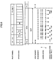
- Fig. 1 is a block diagram of a reception timing detection circuit of a CDMA receiver of a first embodiment of the present invention.
- the reception timing detection circuit of the CDMA receiver comprises an A/D converter 101 for converting a reception signal into a digital reception signal S, a correlator 102 for obtaining a cross-correlation between the digital reception signal S and a known signal series periodically within a predetermined lag (within a delay period), an interpolation filter 103 for re-sampling an output signal R of the correlator 102 at a frequency higher than the sampling frequency of the A/D converter 101, a power calculation section 104 for obtaining the cross-correlation signal power P that has been re-sampled at the interpolation filter 103, an averaging section 105 for averaging the cross-correlation signal power P over a plurality of cycles and a peak detection section 106 for obtaining a peak Popt of the cross-correlation signal power P that has been averaged by the averaging section 105 and determining an optimum reception timing ⁇ opt.
- the transmission/reception signal that reduces power leaking from the band is band limited with a raised cosine filter exhibiting a roll off factor ranging from 10 to 50%.
- the frequency bandwidth of the transmission/reception signal is kept to be 1.1 to 1.5 times more than the chip rate.
- the sampling frequency for the A/D converter 101 should be at least twice the chip rate.
- the in-phase component (I component) and orthogonal component (Q component) of the complex base band signal are A/D converted, respectively to obtain the digital reception signal S.
- the thus obtained digital reception signal S is expressed as a complex number comprising the in-phase component as a real number section and the orthogonal component as an imaginary number section.
- the digital reception signal S obtained through A/D conversion with an I/F signal at a sampling frequency four times higher than the chip rate also has an equivalent value.
- the sampling frequency is the minimum frequency shared by the data demodulation section. Accordingly any further higher frequency can be used for sampling. It is also possible that a correlation is obtained through the analogue circuit and then the output signal of the correlator 102 is A/D converted at the aforementioned sampling frequency.
- Fig. 2 is a time chart representing the respective formats of a transmission signal and a spread code received by the CDMA receiver of Fig. 1 as the reception signal.
- the transmission signal has an L symbol equivalent to 1 slot.
- the Np symbol as the pilot symbol (PL : known code) is inserted to the head of each slot.
- the spreading ratio (the number of chips of the spread code per symbol) is referred to as M.
- the correlator 102 obtains the cross-correlation value Rn( ⁇ ) at the nth slot using the following equation.
- the mobile station is basically expected to return the upstream signal synchronized with the downlink signal from the base station. Accordingly the reception timing is readily predictable for the receiver of the base station. Dispersion of the reception timing is observed in the propagation delay time dependent upon the distance between the base station and the mobile station and synchronous accuracy of the uplink and downlink signals of the mobile unit.
- the wideband system representative of the CDMA method (for example, ranging from 1MHz to 20MHz) is likely to be affected by the propagation delay time rather than the synchronous accuracy of the mobile unit.
- the maximum propagation time can be derived from the time taken for the wave to run between the maximum cell radius covered by a certain base station.
- the minimum value ⁇ min of the delay range Tw can be derived from subtracting a margin from the delay within the receiver by setting the propagation delay to zero.
- the maximum value ⁇ max of the delay range Tw can be derived from adding the margin to the delay within the receiver to the maximum value of the propagation delay. While in the mobile unit, the delay range Tw cannot be obtained in the above manner from the beginning. After synchronizing the clock with the base station by completing the initial synchronization, the delay range can be restricted in the similar manner so that the propagation delay is considered.
- the interpolation filter 103 interpolates a correlation value between 2 samples per chip output from the series cross-correlator 102 so as to calculate the correlation value with higher delay accuracy. It is required to obtain the correlation value at an interval of 1/4 to 1/16 chip conforming to the allowable timing detection difference and sensitivity deterioration.
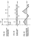
- Fig. 3A The example for obtaining the cross-correlation value with the accuracy of 1/8 chip is described referring to Fig. 3A to 3C.
- Three zeros are inserted between the cross-correlation values at an interval of 1/2 chip (Fig. 3A) output from the correlator 102, respectively so that the signal series at an interval of 1/8 chip is generated (see Fig. 3B).
- the series at an interval of 1/8 chip is subjected to filtering through a low pass filter (LPF) at cut off frequency identical to the chip rate, thus presenting the cross-correlated series having interpolation at each 1/8 chip interval (Fig. 3C).
- LPF low pass filter
- the above impulse response may have a limitless length. Practically it can be restricted to range from +/-1 chip to +/-8 chip by providing a window, allowing for the use of FIR filter.
- the impulse response is restricted to +/- 2 chip, the number of tap of the FIR filter becomes 16 ((8 samples/chip) x 4 chips). As 3 out of 4 samples of the input signal are preliminarily set to zero, adding operation required for calculating the output of 1 sample is executed only 8 times.
- the delay time when the cross-correlation value takes the peak is ultimately required for the output of the reception timing detection circuit.
- the interpolation filter does not have to execute high accurate calculation for obtaining the delay time in the section where the cross-correlation value power is small. That is, the interpolation filter is so controlled not to operate in the section where the cross-correlation value power is smaller than a predetermined threshold value so as to reduce the calculation amount that should be done by the interpolation filter.
- the threshold value governing ON/OFF of the interpolation filter is decided by noise power and peak power of the predicted cross-correlation value as well as the calculation amount required to be reduced and the critical ratio causing detection failure owing to a peak error.
- the threshold can be set to a value smaller than 1/10 of the peak power expected to be twice the noise power.
- a power measurement section 107 measures power of an output R of the correlator 102. Then a comparison section 108 compares the measured power with the threshold value decided as described above. The comparison section 108 outputs a signal for stopping the operation of the interpolation filter 103 in the section where the cross-correlation value power is smaller than the threshold value. Upon receiving the stop signal, the interpolation filter 103 outputs an output R of the correlator 102 as it has been input.
- the phase of the reception signal may become gradually shifted between slots. It is thus impossible to improve Eb/No through in-phase combine that has been applied to the adjacent pilot symbols. So the phase component is removed by obtaining power of the correlation (sum of squares of the I component and Q component) in the power calculation section 104 and then the cross-correlation values between slots within the same delay time period are averaged by the averaging section 105.
- the aforementioned averaging is executed in order to average dispersion owing to noise and variation owing to fading. Taking a large number of averaged slots may reduce dispersion owing to noise. However, the speed for tracking shadowing is decreased. Therefore it is preferable to keep the number of the averaged slot as minimum as possible. In case of a large number of pilot symbols (for example, 16), averaging is not necessarily required.
- the average value can be obtained in several different ways, for example, by splitting into blocks at every predetermined number of slot, obtaining the mobile average through sliding, or obtaining an index weighted mean value.
- Pave n ( ⁇ ) ⁇ ⁇ Pave n ( ⁇ ) + (1 - ⁇ ) ⁇ Pn ( ⁇ ).
- the peak detection circuit 106 obtains the delay time ⁇ opt at which the averaged cross-correlation power Pave n( ⁇ ) takes a maximum value. If the data reception section (not shown) is formed as a RAKE receiver that can combine a plurality of multiple paths in maximum ratio, the peak detection circuit 106 obtains the number of peaks equivalent to that of the RAKE fingers in order of larger size for outputting the delay time ⁇ opt.
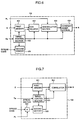
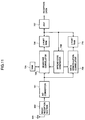
- Fig. 4 is a block diagram of an example of the correlator 102 shown in Fig. 1.
- the correlator 102 comprises a matched filter 201 and a time window section 202.
- the matched filter 201 is the filter matched with the series obtained by spreading the pilot symbol with the spread code. More specifically, it is realized by a FIR filter, taking the complex conjugate series of the aforementioned series as the tap coefficient.
- the time window section 202 selectively allows only a cross-correlation value of the predetermined delay time range Tw to pass through.
- Fig. 5 is a block diagram of another example of the correlator 102 shown in Fig. 1.
- the circuit shown in Fig. 5 is effective only when the spread code length is equivalent to 1 symbol time of the pilot symbol. This type of circuit reduces the operation amount required for cross-correlation compared with the conventional circuit having the spread code length longer than 1 symbol.
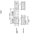
- the correlator 102 comprises a first memory 301 of serial input parallel output type for storing a digital reception signal S for a time period obtained by adding 1 symbol time length of the pilot symbol to the time length of a predetermined delay range, an demodulation section 302 for demodulating the parallel output of the first memory 301 according to the pilot symbol code, an coherent adder section 306 provided with an adder 303 and a memory 304 for coherent adding the demodulated digital reception signal over a plurality of pilot symbols and a correlator 305 for obtaining a cross-correlation between the coherent added digital reception signal and the spread code within a predetermined delay range Tw.
- the size of the first memory 301 is 4M.
- the demodulation circuit 302 multiplies a complex conjugate number of the mth pilot symbol PL(m) at the nth slot with all the above 4M samples.
- the coherent adder 306 accumulation adds each 4M sample output from the demodulation circuit 302 to all Np pilot symbols.
- the head of the slot is cleared to zero and no addition is executed over the slots.
- Fig. 6 is a block diagram of another example of the correlator 102 shown in Fig. 1.
- the correlator 102 comprises a first memory 401 for storing a digital reception signal S for a period obtained by adding a time length of the pilot symbol series to a predetermined time length of the delay range Tw, a second memory 406 for storing a spread code c corresponding to a pilot symbol PL, a correlator 402 for obtaining a cross-correlation per symbol by reading the digital reception signal S and the spread code from the first memory 401 and the second memory 406, respectively, an demodulation section 403 for demodulating the cross-correlation value output from the correlator 402 conforming to the pilot symbol PL, an coherent adder section 404 for accumulation adding the demodulated correlation signals over a plurality of pilot symbols, and a timing control section 405 for controlling the reception timing so that the pilot symbol is contained in the digital reception signal S accumulated in the first memory 401 and controlling to read from the first memory 401 and the second memory 406 repeatedly by sliding the timing until all cross-correlations are
- Fig. 7 is a block diagram of a further example of the correlator 102 shown in Fig. 1.
- this correlator 102 comprises a first memory 501 for storing a digital reception signal S for a period obtained by adding a time length of the pilot symbol series to a time length of a predetermined delay range Tw, a spread section 504 for spreading the pilot symbol PL with a spread code, a second memory 505 for storing the pilot symbol spread by the spread section 504, a correlator 502 for obtaining a cross-correlation by reading the digital reception signal S and the spread pilot symbol from the first memory 501 and the second memory 505, respectively and a timing control section 503 for controlling the reception timing so that the pilot symbol is contained in the digital reception signal S accumulated in the first memory 501 and controlling to read from the first memory 501 and the second memory 505 repeatedly by sliding the timing until all cross-correlations are obtained within the predetermined delay range Tw.
- Each of the correlators 102 shown in Fig. 6 and Fig. 7 is the circuit that can be applied when the spread code has a longer symbol time length, i.e., direct spread using a long code, than 1 symbol time length of the pilot symbol.
- the correlation between the reception data and the spread code is obtained (de-spread) in the same manner as normal data reception and demodulation is executed using a known pilot symbol. Then coherent adding is executed by removing the demodulation component.
- the series in which the pilot symbol is preliminarily spread is obtained and the cross-correlation between the known series and the reception signal is directly obtained.
- the method shown in Fig. 6 can provide the correlation value at every symbol as the result of the middle of the process.
- the circuit shown in Fig. 7 should be better choice because of its simple construction.
- Fig. 8 is a time chart showing the operation of the correlator 102 shown in Fig. 7.
- Fig. 8 represents that the correlator 502 parallel calculates to obtain the cross-correlation with respect to 32 delay times.
- the number of parallel calculation that can be done is defined by a trade-off relationship between the hardware size and the cross-correlation operation time. Therefore an optimum number can be decided by considering the spreading ratio, delay time range for searching the peak, slot cycle, process clock rate and the like.
- 32 units of parallel correlators are used to obtain 4M cross-correlation values.
- the reception signal and the spread pilot symbol series are read from the memories repeatedly by 4M/32 times for executing correlation operation.
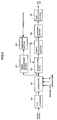
- Fig. 9 is a block diagram showing a reception timing detection circuit of a CDMA receiver of a second embodiment of the present invention.
- the reception timing detection circuit of the CDMA receiver processes decided data obtained by deciding reception data of a reception signal as a known signal instead of using the pilot symbol. That is, the reception timing detection circuit of the CDMA receiver shown in Fig. 9 is identical to the reception timing detection circuit of the CDMA receiver as shown in Fig. 1 except that the known signal input to the correlator 102 is not the pilot symbol but the decided data.
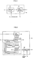
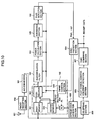
- Fig. 10 is a block diagram of a CDMA receiver comprising the reception timing detection circuit shown in Fig. 1.
- the CDMA receiver comprises the correlator 102 as shown in Fig. 7.
- the CDMA receiver comprises a radio reception section 602 for converting a radio signal received via an antenna 601 into a complex base band signal.
- An A/D converter 101 digitizes the complex base band signal into a digital reception signal.
- a first memory 501 stores the digital reception signal.
- a spread section 504 spreads the pilot symbol PL with a spread code.
- a second memory 505 stores the spread pilot symbol series.
- a correlator 502 reads the digital reception signal and the spread pilot symbol from the first memory 501 and the second memory 505, respectively for obtaining a cross-correlation.
- a power calculation section 104 calculates power of the cross-correlation series that has been interpolated by an interpolation filter 103 as the cross-correlation power.
- An averaging section 105 averages the cross-correlation power within the same delay time over a plurality of slots.
- a peak detection section 106 detects a peak of the averaged cross-correlation power.
- a timing control section 503 controls the respective operation timings of the first and the second memories 501 and 505, correlator 502, interpolation filter 103, power calculation section 104, averaging section 105 and peak detection section 106.
- a spread code generation section 603 generates a spread code and supplies the spread code to the spread section 504 and an de-spread section 605.
- the de-spread section 605 outputs a pre-spread data signal by multiplying a complex conjugate of the spread code by the digital reception signal and integrating the multiplication result by 1 symbol.
- a pilot symbol assisted coherent detection section 606 obtains a reference phase at each symbol timing within the slot through straight interpolation, taking a known pilot symbol inserted to the head of 2 successive slots as a reference signal for coherent detection.
- a RAKE combining section 607 comprising an de-spread section identical to the de-spread section 605 and a plurality of pilot symbol assisted coherent detection sections identical to the pilot symbol assisted coherent detection section 606 outputs reception data by wave detecting each path of the multiple path transmission channel and combining in a maximum ratio.
- a sync. protection section 604 monitors errors of an optimum reception timing ⁇ opt detected by the peak detection section 106, the peak power Popt at the optimum reception timing ⁇ opt and a sync. signal contained in the reception data (The known pilot symbol can be used as the sync. signal.) and controls the spread code generation section 603 and the timing control section 503 so that sync. status is maintained.
- Fig. 11 is a block diagram of another example of the CDMA receiver that realizes the same function as performed by the CDMA receiver as shown in Fig. 10.
- the CDMA receiver comprises the identical elements to those designated as the same reference numerals.
- the CDMA receiver comprises a searcher correlator 705 for storing a correlation series between the digital reception signal and the spread pilot symbol series at each slot in a 2 port RAM 706, a RAM 704 for temporarily storing reception data used by the searcher correlator 705, a spread code generator 708 for generating a spread code and a spread pilot symbol series and supplying them to the searcher correlator 705 and the data demodulation correlator 709, a data demodulation correlator 709 for de-spreading a digital signal to a plurality of multiple path signals with a plurality of RAKE fingers in accordance with a reception delay ordered by a DSP (digital signal processor) 707 and storing the de-spread signal in the 2 port RMA 710 and the DSP 707 for setting an optimum reception timing in the spread code generator 708 by detecting the peak of the cross-correlation series stored in a DSP
- the searcher correlator 705, spread code generator 708 and data demodulation correlator 709 can be formed by a hardware, for example, gate array (G/A), exclusive LSI, and the like. Assuming that the chip rate is set to 4.096 Mcps and the symbol rate to 256 ksps, the exclusive hardware may process the chip rate requiring simple and high-rate processing. While the DSP firmware may realize symbol rate processing requiring relatively a low rate but complex processing. As a result, the most desirable embodiment can be realized.
- G/A gate array
- exclusive LSI exclusive LSI
- a first advantageous effect of the present invention is that the probability and accuracy for appropriately detecting the peak point of the delay profile can be improved even if the Eb/No per path is low. Therefore the appropriate reception timing can be always established, leading to the improved reception quality. Furthermore, as the present invention meets desired reception quality even under the lower Eb/No condition, the capacity of the cellular system using the CDMA and the cell radius covered by 1 base station can be enlarged.
- the delay profile is provided by obtaining a cross-correlation between a known signal and the reception signal over a plurality of symbols or coherent adding over a plurality of symbols (normally the number of pilot symbols per slot). And then the power (sum of squares) is obtained.
- the power of the noise component contained in the cross-correlation value is reduced to 1/(number of pilot symbols), which is smaller than that of the prior art case. Assuming that the number of the pilot symbol per slot is 16, the power of the noise component can be reduced by about 12dB.
- the present invention can completely solve such problem that the cross-correlation value obtained at a moment when the reception level is raised by fading exceeds the cross-correlation value of the correct peak point obtained at a moment when the reception level is low.
- the cross-correlation value is obtained at 1/2 chip interval and then it is obtained at a shorter interval using an interpolation filter. Accordingly more accurate peak point (delay time) of the delay profile can be obtained.
- the present invention greatly improves the accuracy of detecting the reception timing without increasing processing amount.
- a second advantageous effect of the present invention is that the operation amount required for obtaining the peak of the delay profile can be reduced.
- the present invention requires to obtain the correlation value only at 1/2 interval in order to keep deterioration of the Eb/No required to an optimum reception timing to be 1dB or less. While the prior art requires to obtain power of the correlation value at 1/4 interval. Since the noise contained in the cross-correlation value can be reduced, the number of averaging processings for restraining the dispersion of the noise power can also be decreased.
- a third advantageous effect of the present invention is that the size of the hardware used for the base station system can be reduced.
- the power measurement section 107 and comparison section 108 are provided and the interpolation filter 103 is operated at a predetermined threshold value or more.
- the objective of the present invention can be achieved by operating the interpolation filter 103 irrespective of the threshold value under no provision of the power measurement section 107 and comparison section 108.
Applications Claiming Priority (3)
| Application Number | Priority Date | Filing Date | Title |
|---|---|---|---|
| JP185103/96 | 1996-07-15 | ||
| JP18510396A JP2751959B2 (ja) | 1996-07-15 | 1996-07-15 | Cdma受信装置の受信タイミング検出回路 |
| JP18510396 | 1996-07-15 |
Publications (3)
| Publication Number | Publication Date |
|---|---|
| EP0820156A2 true EP0820156A2 (de) | 1998-01-21 |
| EP0820156A3 EP0820156A3 (de) | 2002-10-09 |
| EP0820156B1 EP0820156B1 (de) | 2004-12-15 |
Family
ID=16164914
Family Applications (1)
| Application Number | Title | Priority Date | Filing Date |
|---|---|---|---|
| EP19970111931 Expired - Lifetime EP0820156B1 (de) | 1996-07-15 | 1997-07-14 | Empfangszeiterkennungsschaltung eines CDMA-Empfängers und Verfahren dazu |
Country Status (6)
| Country | Link |
|---|---|
| US (1) | US5982763A (de) |
| EP (1) | EP0820156B1 (de) |
| JP (1) | JP2751959B2 (de) |
| KR (1) | KR100254751B1 (de) |
| CA (1) | CA2210475C (de) |
| DE (1) | DE69731916T2 (de) |
Cited By (24)
| Publication number | Priority date | Publication date | Assignee | Title |
|---|---|---|---|---|
| EP0880238A2 (de) * | 1997-05-21 | 1998-11-25 | Mitsubishi Denki Kabushiki Kaisha | Spreizspektrumsignalempfangsverfahren und -gerät |
| EP0991199A2 (de) * | 1998-09-29 | 2000-04-05 | Nec Corporation | Empfangsschaltung |
| EP1065794A2 (de) * | 1999-06-30 | 2001-01-03 | Nec Corporation | Direktsequenz CDMA-Empfänger mit Verzögerungsprofilberechner mit Interpolationsfunktion |
| DE19929727A1 (de) * | 1999-06-29 | 2001-01-18 | Siemens Ag | Empfangsteil und Verfahren zum Betrieb eines Empfangsteils |
| WO2001006673A1 (fr) * | 1999-07-21 | 2001-01-25 | Nec Corporation | Procede et dispositif de determination de chemin |
| WO2001043300A1 (en) * | 1999-12-10 | 2001-06-14 | Koninklijke Philips Electronics N.V. | Spread spectrum receiver |
| WO2001058040A2 (de) * | 2000-02-04 | 2001-08-09 | Infineon Technologies Ag | Einrichtung zur durchführung von suchprozeduren in einem mobilfunkempfänger |
| EP1135911A1 (de) * | 1998-11-30 | 2001-09-26 | Motorola, Inc. | Verfahren zum feststellen einer optimalen anzahl von komplexen abtastwerten zur kohärenten mittelwertbildung in einem vermittlungssystem |
| EP1158690A2 (de) * | 2000-04-27 | 2001-11-28 | Nec Corporation | Pfadsucherkreislauf in welchem ein empfangenes Signal in eine Mehrzahl von FFT-Fenstern aufgeteilt wird |
| EP1209816A2 (de) * | 2000-11-24 | 2002-05-29 | Kabushiki Kaisha Toshiba | Verfahren und Vorrichtung zur Kodesynchronisierung in einem CDMA-Empfänger |
| WO2002089349A1 (en) * | 2001-04-28 | 2002-11-07 | Koninklijke Philips Electronics N.V. | Method and apparatus for code synchronisation in cdma |
| WO2002103946A2 (en) * | 2001-06-18 | 2002-12-27 | Koninklijke Philips Electronics N.V. | Peak detection with matched filter |
| EP1298813A2 (de) * | 2001-09-26 | 2003-04-02 | Nokia Corporation | Anordnung und Verfahren zum Detektieren eines Synchronisationssignales |
| WO2004004417A1 (de) * | 2002-06-27 | 2004-01-08 | Harman/Becker Automotive Systems Gmbh | Verfahren zur bewertung der empfangsqualität eines stereorundfunkempfängers und stereorundfunkempfänger |
| SG102622A1 (en) * | 2000-04-06 | 2004-03-26 | Ntt Docomo Inc | Apparatus and method for measurement of communication quality in cdma system |
| DE102004059957A1 (de) * | 2004-12-13 | 2006-06-14 | Fraunhofer-Gesellschaft zur Förderung der angewandten Forschung e.V. | Synchronisationsvorrichtung und Vorrichtung zum Erzeugen eines Synchronisationssignals |
| DE102004059946A1 (de) * | 2004-12-13 | 2006-06-14 | Fraunhofer-Gesellschaft zur Förderung der angewandten Forschung e.V. | Vorrichtung und Verfahren zum Ermitteln eines Korrelationsmaximums |
| EP1699154A1 (de) * | 2003-12-26 | 2006-09-06 | ZTE Corporation | Mehrwegesuchverfahren eines codemultiplex-mehrfachzugriffsystems |
| EP1760901A1 (de) * | 2005-09-01 | 2007-03-07 | Telefonaktiebolaget Lm Ericsson | Verfahren und Vorrichtung zur Auswahl von Verzögerungswerten für einen Rake-Empfänger |
| WO2007035737A2 (en) * | 2005-09-15 | 2007-03-29 | Qualcomm Incorporated | Quick detection of signaling in a wireless communication system |
| CN100394702C (zh) * | 2002-07-29 | 2008-06-11 | 汤姆森许可贸易公司 | 扩谱接收机的同步策略和体系结构 |
| EP2326022A1 (de) * | 2009-11-23 | 2011-05-25 | Nxp B.V. | Vorrichtung zur Erfassung eines Streuspektrumsignals |
| EP2458760A1 (de) * | 2009-10-26 | 2012-05-30 | ZTE Corporation | Verfahren und vorrichtung für mehrwegsuche |
| CN101340257B (zh) * | 1999-07-05 | 2013-07-03 | 松下电器产业株式会社 | 无线通信方法、码分多址通信系统和装置、以及通信方法 |
Families Citing this family (98)
| Publication number | Priority date | Publication date | Assignee | Title |
|---|---|---|---|---|
| JP2800796B2 (ja) * | 1996-08-12 | 1998-09-21 | 日本電気株式会社 | Cdma同期捕捉回路 |
| JPH10173630A (ja) | 1996-12-13 | 1998-06-26 | Nec Corp | Cdmaチップ同期回路 |
| JP2853705B2 (ja) * | 1997-05-07 | 1999-02-03 | 日本電気株式会社 | スペクトラム拡散通信受信機 |
| JP2850959B2 (ja) * | 1997-05-12 | 1999-01-27 | 日本電気株式会社 | スペクトラム拡散通信同期捕捉復調装置 |
| JP2861985B2 (ja) * | 1997-06-16 | 1999-02-24 | 日本電気株式会社 | Cdma用高速セルサーチ方式 |
| JP2870526B1 (ja) * | 1997-09-04 | 1999-03-17 | 日本電気株式会社 | Cdma受信装置 |
| US6208632B1 (en) * | 1998-01-29 | 2001-03-27 | Sharp Laboratories Of America | System and method for CDMA channel estimation |
| JPH11251959A (ja) * | 1998-03-05 | 1999-09-17 | Fujitsu Ltd | 干渉キャンセラ装置及び無線通信装置 |
| JP2894342B1 (ja) * | 1998-03-13 | 1999-05-24 | 日本電気株式会社 | スロットタイミング検出方法および検出回路ならびに移動局ならびに移動通信システム |
| JP3891373B2 (ja) * | 1998-03-26 | 2007-03-14 | ソニー株式会社 | 復調装置及び復調方法 |
| JP3484072B2 (ja) * | 1998-04-14 | 2004-01-06 | 株式会社日立国際電気 | 逆拡散回路 |
| US6317422B1 (en) * | 1998-04-15 | 2001-11-13 | Nortel Networks Limited | Methods and apparatus of N-chip resistant spreading in CDMA systems |
| JP3180769B2 (ja) * | 1998-07-17 | 2001-06-25 | 日本電気株式会社 | 受信電力算出方法及び移動局 |
| US6424641B1 (en) * | 1998-08-19 | 2002-07-23 | Nortel Networks Limited | Searcher architecture for CDMA systems |
| US6445714B1 (en) * | 1998-08-19 | 2002-09-03 | Nortel Networks Limited | Code generator for multiple correlators |
| JP3967472B2 (ja) * | 1998-09-07 | 2007-08-29 | 富士通株式会社 | Cdma受信機 |
| JP3883713B2 (ja) | 1998-10-05 | 2007-02-21 | 富士通株式会社 | 拡散符号及びタイミング検出装置及びその方法 |
| US6519300B1 (en) * | 1998-11-12 | 2003-02-11 | Ericsson Inc. | System and method for automatic frequency correction in a pilot symbol assisted demodulator |
| US6256338B1 (en) * | 1998-11-30 | 2001-07-03 | Motorola, Inc. | Method for determining fading correction factor in a communication system |
| JP3264259B2 (ja) * | 1998-12-10 | 2002-03-11 | 日本電気株式会社 | Cdma受信装置 |
| US6678313B1 (en) * | 1998-12-25 | 2004-01-13 | Kokusai Electric Co., Ltd. | Correlation circuit for spread spectrum communication |
| US6424642B1 (en) * | 1998-12-31 | 2002-07-23 | Texas Instruments Incorporated | Estimation of doppler frequency through autocorrelation of pilot symbols |
| JP3156783B2 (ja) * | 1999-01-21 | 2001-04-16 | 日本電気株式会社 | スペクトラム拡散通信システムにおける同期捕捉装置および同期捕捉方法 |
| JP3583006B2 (ja) * | 1999-02-24 | 2004-10-27 | 株式会社日立国際電気 | 符号分割多重アクセス受信機 |
| US7496132B2 (en) * | 1999-03-15 | 2009-02-24 | Kg Electronics Inc. | Pilot signals for synchronization and/or channel estimation |
| US7012906B1 (en) * | 1999-03-15 | 2006-03-14 | Lg Information & Communications, Ltd. | Pilot signals for synchronization and/or channel estimation |
| US6791960B1 (en) | 1999-03-15 | 2004-09-14 | Lg Information And Communications, Ltd. | Pilot signals for synchronization and/or channel estimation |
| KR100294711B1 (ko) * | 1999-03-15 | 2001-07-12 | 서평원 | 최적의 파일럿 심볼을 이용한 프레임 동기 방법 |
| US7643540B2 (en) * | 1999-03-15 | 2010-01-05 | Lg Electronics Inc. | Pilot signals for synchronization and/or channel estimation |
| US6721299B1 (en) * | 1999-03-15 | 2004-04-13 | Lg Information & Communications, Ltd. | Pilot signals for synchronization and/or channel estimation |
| US6574267B1 (en) * | 1999-03-22 | 2003-06-03 | Golden Bridge Technology, Inc. | Rach ramp-up acknowledgement |
| US6169759B1 (en) | 1999-03-22 | 2001-01-02 | Golden Bridge Technology | Common packet channel |
| US6606341B1 (en) | 1999-03-22 | 2003-08-12 | Golden Bridge Technology, Inc. | Common packet channel with firm handoff |
| KR100640337B1 (ko) * | 1999-04-24 | 2006-10-31 | 삼성전자주식회사 | 부호분할 다중접속 방식을 사용하는 이동통신 시스템의 역확산장치 |
| US6314130B1 (en) * | 1999-04-28 | 2001-11-06 | Dspc Technologies, Ltd. | System and method for joint time tracking of multiple paths |
| JP2001016135A (ja) | 1999-06-29 | 2001-01-19 | Nec Corp | 自動周波数制御方法と自動周波数制御方式とcdma受信機 |
| US6765894B1 (en) * | 1999-07-05 | 2004-07-20 | Matsushita Electric Industrial Co, Ltd. | Communication terminal apparatus and base station apparatus |
| JP3344478B2 (ja) | 1999-07-16 | 2002-11-11 | 日本電気株式会社 | Cdmaセルラシステムにおけるパスサーチ回路 |
| KR100346783B1 (ko) * | 1999-07-19 | 2002-08-01 | 한국전자통신연구원 | 보간 필터를 사용한 타이밍 복원장치 및 방법 |
| US6463048B1 (en) * | 1999-07-21 | 2002-10-08 | Lucent Technologies Inc. | Code generator for multiple rake finger and method of use |
| KR100346227B1 (ko) * | 1999-09-18 | 2002-08-01 | 삼성전자 주식회사 | 부호분할다중접속 이동통신시스템에서의 잡음전력 추정장치 및방법 |
| US6996162B1 (en) * | 1999-10-05 | 2006-02-07 | Texas Instruments Incorporated | Correlation using only selected chip position samples in a wireless communication system |
| EP1094619A2 (de) * | 1999-10-20 | 2001-04-25 | Sony Corporation | Signalempfangsvorrichtung für ein GPS-Navigationssystem und ein mobiles Übertragungssystem |
| US6643318B1 (en) | 1999-10-26 | 2003-11-04 | Golden Bridge Technology Incorporated | Hybrid DSMA/CDMA (digital sense multiple access/code division multiple access) method with collision resolution for packet communications |
| US7420986B1 (en) * | 1999-11-02 | 2008-09-02 | Broadcom Corporation | Method and apparatus for the detection and classification of collisions on a shared RF network |
| WO2001039452A1 (en) | 1999-11-29 | 2001-05-31 | Golden Bridge Technology, Inc. | Closed loop power control for common downlink transport channels |
| US6757319B1 (en) | 1999-11-29 | 2004-06-29 | Golden Bridge Technology Inc. | Closed loop power control for common downlink transport channels |
| JP3419726B2 (ja) * | 2000-02-03 | 2003-06-23 | 松下電器産業株式会社 | メモリ回路および同期検波回路 |
| JP4590113B2 (ja) * | 2000-03-14 | 2010-12-01 | キヤノン株式会社 | スペクトラム拡散通信システムのための受信装置 |
| US6449302B2 (en) * | 2000-04-19 | 2002-09-10 | Powerwave Technologies, Inc. | System and method for peak power reduction in spread spectrum communications systems |
| JP2001326584A (ja) | 2000-05-18 | 2001-11-22 | Nec Corp | パス検出方式と受信装置 |
| JP3438701B2 (ja) | 2000-06-09 | 2003-08-18 | 日本電気株式会社 | Ds−cdmaシステムにおける受信パスタイミング検出回路 |
| EP1168654B1 (de) * | 2000-06-28 | 2006-08-16 | Samsung Electronics Co. Ltd. | Pilotkanalleistungsmessungsmittel für eine Mobilstation in einem asynchronen CDMA-Kommunikationssystem |
| JP2002026767A (ja) | 2000-07-04 | 2002-01-25 | Nec Corp | Cdma受信装置及びパス検出方法 |
| US6728301B1 (en) | 2000-07-07 | 2004-04-27 | Texas Instruments Incorporated | System and method for automatic frequency control in spread spectrum communications |
| DE60137657D1 (en) * | 2000-08-03 | 2009-03-26 | Infineon Technologies Ag | Flexible tdma systemarchitektur |
| DE60131824T2 (de) * | 2000-11-01 | 2008-11-27 | Ntt Docomo Inc. | Rückgewinnung des Symboltaktes |
| US6424673B1 (en) * | 2000-11-10 | 2002-07-23 | Motorola, Inc. | Method and apparatus in a wireless communication system for facilitating detection of, and synchronization with, a predetermined synchronization signal |
| US6985516B1 (en) * | 2000-11-27 | 2006-01-10 | Qualcomm Incorporated | Method and apparatus for processing a received signal in a communications system |
| KR100488078B1 (ko) * | 2000-12-21 | 2005-05-09 | 엘지전자 주식회사 | 이동 통신 시스템 수신단의 파일럿 신호 검색기 및 방법 |
| JP4558225B2 (ja) * | 2001-02-15 | 2010-10-06 | 株式会社日立国際電気 | 符号分割多重アクセス受信機 |
| US20030133430A1 (en) * | 2001-05-31 | 2003-07-17 | Dickson William D. | Efficient method of improving detection of signals containing repetitive components |
| US7104534B2 (en) | 2001-06-08 | 2006-09-12 | Broadcom Corporation | System and method for detecting collisions in a shared communications medium |
| SG108257A1 (en) * | 2001-06-15 | 2005-01-28 | Oki Electric Ind Co Ltd | Receiving circuit |
| JP2003198427A (ja) * | 2001-12-28 | 2003-07-11 | Fujitsu Ltd | Cdma受信装置 |
| KR100431083B1 (ko) * | 2002-01-25 | 2004-05-12 | 한국전자통신연구원 | 구간 검색기 및 그의 구동 방법과 이를 이용한 코드 검색기 |
| US7324584B1 (en) * | 2002-01-31 | 2008-01-29 | Nortel Networks Limited | Low complexity interference cancellation |
| US6792037B2 (en) * | 2002-02-28 | 2004-09-14 | Interdigital Technology Corporation | Apparatus and method of searching for known sequences |
| WO2003075481A1 (en) * | 2002-03-05 | 2003-09-12 | Koninklijke Philips Electronics N.V. | Mobile terminal with down-link synchronisation via an iterative correlation system |
| FI116179B (fi) * | 2002-03-13 | 2005-09-30 | Nokia Corp | Menetelmä ja järjestelmä etenemisviiveen määrittämiseksi sekä elektroniikkalaite |
| JP4012444B2 (ja) | 2002-08-06 | 2007-11-21 | 松下電器産業株式会社 | 遅延プロファイル作成方法および遅延プロファイル作成装置 |
| JP4052060B2 (ja) | 2002-08-21 | 2008-02-27 | 日本電気株式会社 | Cdma無線装置及びそれに用いる簡易パス推定方法 |
| FR2845217B1 (fr) * | 2002-09-27 | 2004-12-17 | St Microelectronics Sa | Procede de traitement d'un signal incident au sein d'un recepteur "rake" a plusieurs doigts, et recepteur "rake" correspondant |
| KR20040037473A (ko) * | 2002-10-28 | 2004-05-07 | 엘지전자 주식회사 | 이동 통신 시스템의 초기 동기 방법 |
| KR100979151B1 (ko) * | 2002-11-22 | 2010-08-31 | 인터디지탈 테크날러지 코포레이션 | 복소 가중치 생성(cwg) 알고리즘을 이용한 레이크 수신기에서의 채널 이득 추정 |
| US20040125865A1 (en) * | 2002-12-30 | 2004-07-01 | Frank Colin D. | Maximum signal-to-interference-and-noise spread spectrum rake receiver and method |
| US7336699B2 (en) * | 2003-02-19 | 2008-02-26 | Analog Devices, Inc. | Method and apparatus for code identification in wireless applications |
| JP2005086585A (ja) * | 2003-09-10 | 2005-03-31 | Nec Corp | 通信装置及びそれに用いる基地局サーチ方法並びにそのプログラム |
| US7336739B2 (en) * | 2003-09-26 | 2008-02-26 | Lockheed Martin Corporation | Cross-correlation signal detector |
| US20050169353A1 (en) * | 2004-02-02 | 2005-08-04 | Wei An | Post despreading interpolation in CDMA systems |
| JP4448403B2 (ja) * | 2004-08-16 | 2010-04-07 | 富士通株式会社 | 電力レベル測定装置及び移動局 |
| JP4308105B2 (ja) * | 2004-08-23 | 2009-08-05 | Okiセミコンダクタ株式会社 | 同期追従回路 |
| KR100771194B1 (ko) * | 2005-08-29 | 2007-10-30 | 삼성탈레스 주식회사 | 직접 시퀀스 확산 대역 버스트 무선 통신 시스템에서타이밍 동기를 획득하는 장치 |
| US8594151B2 (en) * | 2005-10-31 | 2013-11-26 | Nokia Corporation | Pilot sequence detection |
| US7995676B2 (en) * | 2006-01-27 | 2011-08-09 | The Mitre Corporation | Interpolation processing for enhanced signal acquisition |
| JP4837403B2 (ja) * | 2006-03-08 | 2011-12-14 | ルネサスエレクトロニクス株式会社 | 同期タイミング検出装置、受信装置、及び同期タイミング検出方法 |
| EP2003789B1 (de) * | 2006-03-31 | 2016-05-18 | Fujitsu Limited | Cdma-empfänger und cdma-empfangsverfahren |
| US8170087B2 (en) * | 2007-05-10 | 2012-05-01 | Texas Instruments Incorporated | Correlation coprocessor |
| JP5499435B2 (ja) * | 2007-11-20 | 2014-05-21 | セイコーエプソン株式会社 | 相互相関判定方法、測位装置及び電子機器 |
| US8204377B2 (en) * | 2008-10-23 | 2012-06-19 | Alcatel Lucent | System, method and apparatus for joint self phase modulation compensation for coherent optical polarization-division-multiplexed orthogonal-frequency division-multiplexing systems |
| JP2011003970A (ja) * | 2009-06-16 | 2011-01-06 | Fujitsu Ltd | 受信装置、基地局装置及び同期タイミング検出方法 |
| JP5423505B2 (ja) * | 2010-03-17 | 2014-02-19 | 富士通株式会社 | 無線基地局及び通信方法 |
| US9490867B2 (en) | 2011-08-16 | 2016-11-08 | Harris Corporation | CDMA communications device and related methods |
| US8768275B2 (en) * | 2011-11-10 | 2014-07-01 | National Instruments Corporation | Spectral averaging |
| US9621205B2 (en) * | 2015-03-26 | 2017-04-11 | Vt Idirect, Inc. | Apparatus and method for frequency estimation ambiguity removal of a burst signal |
| KR101594450B1 (ko) * | 2015-05-06 | 2016-02-16 | 국방과학연구소 | 입력 신호의 상호 상관을 수행하는 방법 |
| CN112887235B (zh) * | 2020-12-30 | 2022-11-29 | 鹤壁天海电子信息系统有限公司 | 接收信号的干扰检测方法、终端及存储装置 |
| CN113543298B (zh) * | 2021-06-07 | 2022-09-02 | 中国联合网络通信集团有限公司 | 定时同步方法及基站 |
Citations (1)
| Publication number | Priority date | Publication date | Assignee | Title |
|---|---|---|---|---|
| GB2298342A (en) * | 1995-02-16 | 1996-08-28 | Roke Manor Research | Apparatus for acquiring code phase lock in direct sequence spread spectrum systems |
Family Cites Families (6)
| Publication number | Priority date | Publication date | Assignee | Title |
|---|---|---|---|---|
| JP2692434B2 (ja) * | 1991-02-22 | 1997-12-17 | 三菱電機株式会社 | スペクトル拡散復調装置 |
| JPH06277227A (ja) * | 1993-03-26 | 1994-10-04 | Toshiba Medical Eng Co Ltd | レーザ治療装置 |
| WO1996021294A1 (fr) * | 1995-01-05 | 1996-07-11 | Ntt Mobile Communications Network Inc. | Procede et dispositif de poursuite coherente d'un recepteur a acces multiple par code de repartition |
| FI101256B (fi) * | 1995-10-03 | 1998-05-15 | Nokia Mobile Phones Ltd | Menetelmä vastaanotetun signaalin ajoituksen mittaamiseksi tiedonsiirt ojärjestelmässä ja menetelmän toteuttava matkaviestin |
| JP3273539B2 (ja) * | 1996-01-19 | 2002-04-08 | シャープ株式会社 | スペクトル拡散信号受信機 |
| US5799038A (en) * | 1996-04-30 | 1998-08-25 | Advantest Corporation | Method for measuring modulation parameters of digital quadrature-modulated signal |
-
1996
- 1996-07-15 JP JP18510396A patent/JP2751959B2/ja not_active Expired - Lifetime
-
1997
- 1997-07-14 DE DE1997631916 patent/DE69731916T2/de not_active Expired - Lifetime
- 1997-07-14 US US08/892,497 patent/US5982763A/en not_active Expired - Lifetime
- 1997-07-14 EP EP19970111931 patent/EP0820156B1/de not_active Expired - Lifetime
- 1997-07-15 KR KR1019970032740A patent/KR100254751B1/ko not_active IP Right Cessation
- 1997-07-15 CA CA002210475A patent/CA2210475C/en not_active Expired - Fee Related
Patent Citations (1)
| Publication number | Priority date | Publication date | Assignee | Title |
|---|---|---|---|---|
| GB2298342A (en) * | 1995-02-16 | 1996-08-28 | Roke Manor Research | Apparatus for acquiring code phase lock in direct sequence spread spectrum systems |
Non-Patent Citations (3)
| Title |
|---|
| ANDREW J. VITERBI: "Principles of Spread Spectrum Communication" , ADDISON-WESLEY PUBLISHING COMPANY , APRIL 1995 XP002201837 * page 52, paragraph 3.4 - page 67, paragraph 3.6 * * |
| GIANNETTI F ET AL: "Design of an all-digital receiver for narrowband continuous-phase asynchronous CDMA systems" PROCEEDINGS OF THE INTERNATIONAL CONFERENCE ON COMMUNICATIONS (ICC). GENEVA, MAY 23 - 26, 1993, NEW YORK, IEEE, US, vol. 3, 23 May 1993 (1993-05-23), pages 468-472, XP010136945 ISBN: 0-7803-0950-2 * |
| JONES W W ET AL: "Post acquisition PN code uncertainty reduction by least-squares interpolation" MILITARY COMMUNICATIONS IN A CHANGING WORLD. MCLEAN, VA., NOV. 4 - 7, 1991, PROCEEDINGS OF THE MILITARY COMMUNICATIONS CONFERENCE. (MILCOM), NEW YORK, IEEE, US, vol. 2, 4 November 1991 (1991-11-04), pages 804-808, XP010042260 ISBN: 0-87942-691-8 * |
Cited By (56)
| Publication number | Priority date | Publication date | Assignee | Title |
|---|---|---|---|---|
| EP0880238A3 (de) * | 1997-05-21 | 2002-10-23 | Mitsubishi Denki Kabushiki Kaisha | Spreizspektrumsignalempfangsverfahren und -gerät |
| EP0880238A2 (de) * | 1997-05-21 | 1998-11-25 | Mitsubishi Denki Kabushiki Kaisha | Spreizspektrumsignalempfangsverfahren und -gerät |
| EP0991199A2 (de) * | 1998-09-29 | 2000-04-05 | Nec Corporation | Empfangsschaltung |
| US6768769B2 (en) | 1998-09-29 | 2004-07-27 | Nec Corporation | Receiving circuit, mobile terminal with receiving circuit, and method of receiving data |
| EP0991199A3 (de) * | 1998-09-29 | 2003-10-22 | Nec Corporation | Empfangsschaltung |
| EP1135911A1 (de) * | 1998-11-30 | 2001-09-26 | Motorola, Inc. | Verfahren zum feststellen einer optimalen anzahl von komplexen abtastwerten zur kohärenten mittelwertbildung in einem vermittlungssystem |
| EP1135911A4 (de) * | 1998-11-30 | 2003-01-08 | Motorola Inc | Verfahren zum feststellen einer optimalen anzahl von komplexen abtastwerten zur kohärenten mittelwertbildung in einem vermittlungssystem |
| DE19929727A1 (de) * | 1999-06-29 | 2001-01-18 | Siemens Ag | Empfangsteil und Verfahren zum Betrieb eines Empfangsteils |
| DE19929727C2 (de) * | 1999-06-29 | 2003-01-30 | Siemens Ag | Empfangsteil zum Betrieb eines Empfangsteils |
| US6816542B1 (en) | 1999-06-30 | 2004-11-09 | Nec Corporation | Direct sequence CDMA receiver having a delay profile producer with an interpolation function |
| EP1065794A3 (de) * | 1999-06-30 | 2003-01-02 | Nec Corporation | Direktsequenz CDMA-Empfänger mit Verzögerungsprofilberechner mit Interpolationsfunktion |
| EP1065794A2 (de) * | 1999-06-30 | 2001-01-03 | Nec Corporation | Direktsequenz CDMA-Empfänger mit Verzögerungsprofilberechner mit Interpolationsfunktion |
| CN101340257B (zh) * | 1999-07-05 | 2013-07-03 | 松下电器产业株式会社 | 无线通信方法、码分多址通信系统和装置、以及通信方法 |
| US7042862B1 (en) | 1999-07-21 | 2006-05-09 | Nec Corporation | Path searching method and device |
| WO2001006673A1 (fr) * | 1999-07-21 | 2001-01-25 | Nec Corporation | Procede et dispositif de determination de chemin |
| EP1381169A1 (de) * | 1999-07-21 | 2004-01-14 | NEC Corporation | Verfahren und Vorrichtung zur Pfadsuche |
| US6611550B1 (en) | 1999-12-10 | 2003-08-26 | Koninklijke Philips Electronics N.V. | Spread spectrum receiver |
| WO2001043300A1 (en) * | 1999-12-10 | 2001-06-14 | Koninklijke Philips Electronics N.V. | Spread spectrum receiver |
| US6650690B2 (en) | 2000-02-04 | 2003-11-18 | Infineon Technologies Ag | Device and system for carrying out search procedures in a mobile radio receiver |
| WO2001058040A3 (de) * | 2000-02-04 | 2002-02-14 | Infineon Technologies Ag | Einrichtung zur durchführung von suchprozeduren in einem mobilfunkempfänger |
| WO2001058040A2 (de) * | 2000-02-04 | 2001-08-09 | Infineon Technologies Ag | Einrichtung zur durchführung von suchprozeduren in einem mobilfunkempfänger |
| US7050482B2 (en) | 2000-04-06 | 2006-05-23 | Ntt Docomo, Inc. | Apparatus and method for measurement of communication quality in CDMA system |
| US7333529B2 (en) | 2000-04-06 | 2008-02-19 | Ntt Docomo, Inc. | Apparatus and method for measurement of communication quality in CDMA system |
| CN100566193C (zh) * | 2000-04-06 | 2009-12-02 | 株式会社Ntt都科摩 | 码分多址系统中通信质量测量的方法与装置 |
| SG102622A1 (en) * | 2000-04-06 | 2004-03-26 | Ntt Docomo Inc | Apparatus and method for measurement of communication quality in cdma system |
| EP1158690A3 (de) * | 2000-04-27 | 2004-03-31 | Nec Corporation | Pfadsucherkreislauf in welchem ein empfangenes Signal in eine Mehrzahl von FFT-Fenstern aufgeteilt wird |
| EP1158690A2 (de) * | 2000-04-27 | 2001-11-28 | Nec Corporation | Pfadsucherkreislauf in welchem ein empfangenes Signal in eine Mehrzahl von FFT-Fenstern aufgeteilt wird |
| US7068709B2 (en) | 2000-11-24 | 2006-06-27 | Kabushiki Kaisha Toshiba | Code synchronous timing determining method upon information reception in CDMA system, determining apparatus, and CDMA receiving apparatus |
| EP1209816A3 (de) * | 2000-11-24 | 2004-09-22 | Kabushiki Kaisha Toshiba | Verfahren und Vorrichtung zur Kodesynchronisierung in einem CDMA-Empfänger |
| EP1209816A2 (de) * | 2000-11-24 | 2002-05-29 | Kabushiki Kaisha Toshiba | Verfahren und Vorrichtung zur Kodesynchronisierung in einem CDMA-Empfänger |
| WO2002089349A1 (en) * | 2001-04-28 | 2002-11-07 | Koninklijke Philips Electronics N.V. | Method and apparatus for code synchronisation in cdma |
| WO2002103946A3 (en) * | 2001-06-18 | 2004-04-22 | Koninkl Philips Electronics Nv | Peak detection with matched filter |
| WO2002103946A2 (en) * | 2001-06-18 | 2002-12-27 | Koninklijke Philips Electronics N.V. | Peak detection with matched filter |
| EP1298813A2 (de) * | 2001-09-26 | 2003-04-02 | Nokia Corporation | Anordnung und Verfahren zum Detektieren eines Synchronisationssignales |
| US7092469B1 (en) | 2001-09-26 | 2006-08-15 | Nokia Corporation | Synchronization signal detector and method of detection of synchronization signal |
| EP1298813A3 (de) * | 2001-09-26 | 2003-10-01 | Nokia Corporation | Anordnung und Verfahren zum Detektieren eines Synchronisationssignales |
| WO2004004417A1 (de) * | 2002-06-27 | 2004-01-08 | Harman/Becker Automotive Systems Gmbh | Verfahren zur bewertung der empfangsqualität eines stereorundfunkempfängers und stereorundfunkempfänger |
| CN100394702C (zh) * | 2002-07-29 | 2008-06-11 | 汤姆森许可贸易公司 | 扩谱接收机的同步策略和体系结构 |
| EP1699154A1 (de) * | 2003-12-26 | 2006-09-06 | ZTE Corporation | Mehrwegesuchverfahren eines codemultiplex-mehrfachzugriffsystems |
| CN1879338B (zh) * | 2003-12-26 | 2010-05-12 | 中兴通讯股份有限公司 | 码分多址通信系统的多径搜索方法 |
| EP1699154A4 (de) * | 2003-12-26 | 2007-05-09 | Zte Corp | Mehrwegesuchverfahren eines codemultiplex-mehrfachzugriffsystems |
| DE102004059957A1 (de) * | 2004-12-13 | 2006-06-14 | Fraunhofer-Gesellschaft zur Förderung der angewandten Forschung e.V. | Synchronisationsvorrichtung und Vorrichtung zum Erzeugen eines Synchronisationssignals |
| US7653166B2 (en) | 2004-12-13 | 2010-01-26 | Fraunhofer-Gesellschaft Zur Foerderung Der Angewandten Forschung E.V. | Synchronization device and device for generating a synchronization signal |
| DE102004059946B4 (de) * | 2004-12-13 | 2008-10-02 | Fraunhofer-Gesellschaft zur Förderung der angewandten Forschung e.V. | Vorrichtung und Verfahren zum Ermitteln eines Korrelationsmaximums |
| US7525483B2 (en) | 2004-12-13 | 2009-04-28 | Fraunhofer-Gesellschaft Zur Foerderung Der Angewandten Forschung E.V. | Receive device and method for receiving a receive sequence |
| DE102004059946A1 (de) * | 2004-12-13 | 2006-06-14 | Fraunhofer-Gesellschaft zur Förderung der angewandten Forschung e.V. | Vorrichtung und Verfahren zum Ermitteln eines Korrelationsmaximums |
| US7649936B2 (en) | 2004-12-13 | 2010-01-19 | Fraunhofer-Gesellschaft Zur Foerderung Der Angewandten Forschung E.V. | Device and method for determining a correlation maximum |
| US8064497B2 (en) | 2005-09-01 | 2011-11-22 | Telefonaktiebolaget L M Ericsson (Publ) | Selecting delay values for a rake receiver |
| EP1760901A1 (de) * | 2005-09-01 | 2007-03-07 | Telefonaktiebolaget Lm Ericsson | Verfahren und Vorrichtung zur Auswahl von Verzögerungswerten für einen Rake-Empfänger |
| US8027373B2 (en) | 2005-09-15 | 2011-09-27 | Qualcomm Incorporated | Quick detection of signaling in a wireless communication system |
| WO2007035737A3 (en) * | 2005-09-15 | 2007-05-31 | Qualcomm Inc | Quick detection of signaling in a wireless communication system |
| US8170084B2 (en) | 2005-09-15 | 2012-05-01 | Qualcomm Incorporated | Quick detection of signaling in a wireless communication system |
| WO2007035737A2 (en) * | 2005-09-15 | 2007-03-29 | Qualcomm Incorporated | Quick detection of signaling in a wireless communication system |
| EP2458760A1 (de) * | 2009-10-26 | 2012-05-30 | ZTE Corporation | Verfahren und vorrichtung für mehrwegsuche |
| EP2458760A4 (de) * | 2009-10-26 | 2014-03-26 | Zte Corp | Verfahren und vorrichtung für mehrwegsuche |
| EP2326022A1 (de) * | 2009-11-23 | 2011-05-25 | Nxp B.V. | Vorrichtung zur Erfassung eines Streuspektrumsignals |
Also Published As
| Publication number | Publication date |
|---|---|
| US5982763A (en) | 1999-11-09 |
| KR980012987A (ko) | 1998-04-30 |
| JPH1032523A (ja) | 1998-02-03 |
| CA2210475C (en) | 2000-10-17 |
| KR100254751B1 (ko) | 2000-05-01 |
| CA2210475A1 (en) | 1998-01-15 |
| EP0820156B1 (de) | 2004-12-15 |
| DE69731916T2 (de) | 2005-05-25 |
| JP2751959B2 (ja) | 1998-05-18 |
| DE69731916D1 (de) | 2005-01-20 |
| EP0820156A3 (de) | 2002-10-09 |
Similar Documents
| Publication | Publication Date | Title |
|---|---|---|
| EP0820156B1 (de) | Empfangszeiterkennungsschaltung eines CDMA-Empfängers und Verfahren dazu | |
| EP1158690B1 (de) | Pfadsucherkreislauf in welchem ein empfangenes Signal in eine Mehrzahl von FFT-Fenstern aufgeteilt wird | |
| US6154487A (en) | Spread-spectrum signal receiving method and spread-spectrum signal receiving apparatus | |
| EP0848503B1 (de) | CDMA chip Synchronisationsschaltung | |
| AU756608B2 (en) | Multipath propagation delay determining means using periodically inserted pilot symbols | |
| US7167456B2 (en) | Apparatus for estimating propagation path characteristics | |
| JP3159378B2 (ja) | スペクトル拡散通信方式 | |
| US7142587B2 (en) | Received path timing detecting circuit at DS-CDMA system | |
| US7042862B1 (en) | Path searching method and device | |
| JP3471756B2 (ja) | Cdma通信システムの非直交雑音測定装置及び方法 | |
| US7106783B2 (en) | Method and apparatus for searching multipaths of mobile communication system | |
| KR100651505B1 (ko) | 직접시퀀스 부호분할다중접속 통신시스템에서 다중 경로환경에서의 코드 추적 장치 및 방법 | |
| KR20030044067A (ko) | 수신기 및 수신 방법 | |
| US6775341B2 (en) | Time recovery circuit and method for synchronizing timing of a signal in a receiver to timing of the signal in a transmitter |
Legal Events
| Date | Code | Title | Description |
|---|---|---|---|
| PUAI | Public reference made under article 153(3) epc to a published international application that has entered the european phase |
Free format text: ORIGINAL CODE: 0009012 |
|
| AK | Designated contracting states |
Kind code of ref document: A2 Designated state(s): AT BE CH DE DK ES FI FR GB GR IE IT LI LU MC NL PT SE |
|
| PUAL | Search report despatched |
Free format text: ORIGINAL CODE: 0009013 |
|
| AK | Designated contracting states |
Kind code of ref document: A3 Designated state(s): AT BE CH DE DK ES FI FR GB GR IE IT LI LU MC NL PT SE |
|
| 17P | Request for examination filed |
Effective date: 20020830 |
|
| AKX | Designation fees paid |
Designated state(s): DE GB SE |
|
| 17Q | First examination report despatched |
Effective date: 20030714 |
|
| GRAP | Despatch of communication of intention to grant a patent |
Free format text: ORIGINAL CODE: EPIDOSNIGR1 |
|
| GRAS | Grant fee paid |
Free format text: ORIGINAL CODE: EPIDOSNIGR3 |
|
| GRAA | (expected) grant |
Free format text: ORIGINAL CODE: 0009210 |
|
| AK | Designated contracting states |
Kind code of ref document: B1 Designated state(s): DE GB SE |
|
| REG | Reference to a national code |
Ref country code: GB Ref legal event code: FG4D |
|
| REG | Reference to a national code |
Ref country code: IE Ref legal event code: FG4D |
|
| REF | Corresponds to: |
Ref document number: 69731916 Country of ref document: DE Date of ref document: 20050120 Kind code of ref document: P |
|
| PLBE | No opposition filed within time limit |
Free format text: ORIGINAL CODE: 0009261 |
|
| STAA | Information on the status of an ep patent application or granted ep patent |
Free format text: STATUS: NO OPPOSITION FILED WITHIN TIME LIMIT |
|
| 26N | No opposition filed |
Effective date: 20050916 |
|
| PGFP | Annual fee paid to national office [announced via postgrant information from national office to epo] |
Ref country code: GB Payment date: 20140709 Year of fee payment: 18 |
|
| PGFP | Annual fee paid to national office [announced via postgrant information from national office to epo] |
Ref country code: DE Payment date: 20150707 Year of fee payment: 19 |
|
| PGFP | Annual fee paid to national office [announced via postgrant information from national office to epo] |
Ref country code: SE Payment date: 20150713 Year of fee payment: 19 |
|
| GBPC | Gb: european patent ceased through non-payment of renewal fee |
Effective date: 20150714 |
|
| PG25 | Lapsed in a contracting state [announced via postgrant information from national office to epo] |
Ref country code: GB Free format text: LAPSE BECAUSE OF NON-PAYMENT OF DUE FEES Effective date: 20150714 |
|
| REG | Reference to a national code |
Ref country code: DE Ref legal event code: R119 Ref document number: 69731916 Country of ref document: DE |
|
| REG | Reference to a national code |
Ref country code: SE Ref legal event code: EUG |
|
| PG25 | Lapsed in a contracting state [announced via postgrant information from national office to epo] |
Ref country code: DE Free format text: LAPSE BECAUSE OF NON-PAYMENT OF DUE FEES Effective date: 20170201 Ref country code: SE Free format text: LAPSE BECAUSE OF NON-PAYMENT OF DUE FEES Effective date: 20160715 |