EP0812468B1 - A METHOD OF MANUFACTURING A HIGH VOLTAGE GaN-AlN BASED SEMICONDUCTOR DEVICE AND SEMICONDUCTOR DEVICE MADE - Google Patents
A METHOD OF MANUFACTURING A HIGH VOLTAGE GaN-AlN BASED SEMICONDUCTOR DEVICE AND SEMICONDUCTOR DEVICE MADE Download PDFInfo
- Publication number
- EP0812468B1 EP0812468B1 EP96939258A EP96939258A EP0812468B1 EP 0812468 B1 EP0812468 B1 EP 0812468B1 EP 96939258 A EP96939258 A EP 96939258A EP 96939258 A EP96939258 A EP 96939258A EP 0812468 B1 EP0812468 B1 EP 0812468B1
- Authority
- EP
- European Patent Office
- Prior art keywords
- layer
- gan
- aln
- conductivity type
- type
- Prior art date
- Legal status (The legal status is an assumption and is not a legal conclusion. Google has not performed a legal analysis and makes no representation as to the accuracy of the status listed.)
- Expired - Lifetime
Links
Images

Classifications
-
- H—ELECTRICITY
- H10—SEMICONDUCTOR DEVICES; ELECTRIC SOLID-STATE DEVICES NOT OTHERWISE PROVIDED FOR
- H10D—INORGANIC ELECTRIC SEMICONDUCTOR DEVICES
- H10D64/00—Electrodes of devices having potential barriers
- H10D64/60—Electrodes characterised by their materials
- H10D64/66—Electrodes having a conductor capacitively coupled to a semiconductor by an insulator, e.g. MIS electrodes
- H10D64/68—Electrodes having a conductor capacitively coupled to a semiconductor by an insulator, e.g. MIS electrodes characterised by the insulator, e.g. by the gate insulator
- H10D64/693—Electrodes having a conductor capacitively coupled to a semiconductor by an insulator, e.g. MIS electrodes characterised by the insulator, e.g. by the gate insulator the insulator comprising nitrogen, e.g. nitrides, oxynitrides or nitrogen-doped materials
-
- H—ELECTRICITY
- H01—ELECTRIC ELEMENTS
- H01L—SEMICONDUCTOR DEVICES NOT COVERED BY CLASS H10
- H01L21/00—Processes or apparatus adapted for the manufacture or treatment of semiconductor or solid state devices or of parts thereof
- H01L21/02—Manufacture or treatment of semiconductor devices or of parts thereof
- H01L21/04—Manufacture or treatment of semiconductor devices or of parts thereof the devices having potential barriers, e.g. a PN junction, depletion layer or carrier concentration layer
- H01L21/18—Manufacture or treatment of semiconductor devices or of parts thereof the devices having potential barriers, e.g. a PN junction, depletion layer or carrier concentration layer the devices having semiconductor bodies comprising elements of Group IV of the Periodic Table or AIIIBV compounds with or without impurities, e.g. doping materials
- H01L21/28—Manufacture of electrodes on semiconductor bodies using processes or apparatus not provided for in groups H01L21/20 - H01L21/268
- H01L21/283—Deposition of conductive or insulating materials for electrodes conducting electric current
- H01L21/285—Deposition of conductive or insulating materials for electrodes conducting electric current from a gas or vapour, e.g. condensation
- H01L21/28506—Deposition of conductive or insulating materials for electrodes conducting electric current from a gas or vapour, e.g. condensation of conductive layers
- H01L21/28575—Deposition of conductive or insulating materials for electrodes conducting electric current from a gas or vapour, e.g. condensation of conductive layers on semiconductor bodies comprising AIIIBV compounds
- H01L21/28587—Deposition of conductive or insulating materials for electrodes conducting electric current from a gas or vapour, e.g. condensation of conductive layers on semiconductor bodies comprising AIIIBV compounds characterised by the sectional shape, e.g. T, inverted T
- H01L21/28593—Deposition of conductive or insulating materials for electrodes conducting electric current from a gas or vapour, e.g. condensation of conductive layers on semiconductor bodies comprising AIIIBV compounds characterised by the sectional shape, e.g. T, inverted T asymmetrical sectional shape
-
- H—ELECTRICITY
- H10—SEMICONDUCTOR DEVICES; ELECTRIC SOLID-STATE DEVICES NOT OTHERWISE PROVIDED FOR
- H10D—INORGANIC ELECTRIC SEMICONDUCTOR DEVICES
- H10D30/00—Field-effect transistors [FET]
- H10D30/01—Manufacture or treatment
- H10D30/015—Manufacture or treatment of FETs having heterojunction interface channels or heterojunction gate electrodes, e.g. HEMT
-
- H—ELECTRICITY
- H10—SEMICONDUCTOR DEVICES; ELECTRIC SOLID-STATE DEVICES NOT OTHERWISE PROVIDED FOR
- H10D—INORGANIC ELECTRIC SEMICONDUCTOR DEVICES
- H10D30/00—Field-effect transistors [FET]
- H10D30/60—Insulated-gate field-effect transistors [IGFET]
- H10D30/67—Thin-film transistors [TFT]
- H10D30/674—Thin-film transistors [TFT] characterised by the active materials
- H10D30/675—Group III-V materials, Group II-VI materials, Group IV-VI materials, selenium or tellurium
-
- H—ELECTRICITY
- H10—SEMICONDUCTOR DEVICES; ELECTRIC SOLID-STATE DEVICES NOT OTHERWISE PROVIDED FOR
- H10D—INORGANIC ELECTRIC SEMICONDUCTOR DEVICES
- H10D30/00—Field-effect transistors [FET]
- H10D30/80—FETs having rectifying junction gate electrodes
- H10D30/801—FETs having heterojunction gate electrodes
-
- H—ELECTRICITY
- H10—SEMICONDUCTOR DEVICES; ELECTRIC SOLID-STATE DEVICES NOT OTHERWISE PROVIDED FOR
- H10D—INORGANIC ELECTRIC SEMICONDUCTOR DEVICES
- H10D62/00—Semiconductor bodies, or regions thereof, of devices having potential barriers
- H10D62/10—Shapes, relative sizes or dispositions of the regions of the semiconductor bodies; Shapes of the semiconductor bodies
- H10D62/17—Semiconductor regions connected to electrodes not carrying current to be rectified, amplified or switched, e.g. channel regions
- H10D62/351—Substrate regions of field-effect devices
- H10D62/357—Substrate regions of field-effect devices of FETs
- H10D62/364—Substrate regions of field-effect devices of FETs of IGFETs
-
- H10D64/0125—
-
- H10D64/0126—
-
- H—ELECTRICITY
- H10—SEMICONDUCTOR DEVICES; ELECTRIC SOLID-STATE DEVICES NOT OTHERWISE PROVIDED FOR
- H10D—INORGANIC ELECTRIC SEMICONDUCTOR DEVICES
- H10D62/00—Semiconductor bodies, or regions thereof, of devices having potential barriers
- H10D62/80—Semiconductor bodies, or regions thereof, of devices having potential barriers characterised by the materials
- H10D62/85—Semiconductor bodies, or regions thereof, of devices having potential barriers characterised by the materials being Group III-V materials, e.g. GaAs
- H10D62/8503—Nitride Group III-V materials, e.g. AlN or GaN
Definitions
- the present invention involves the structure and formation of a Field Effect Transistor semiconductor device, in particular for high voltages which in particular has GaN or AlN based p-n junction features.
- GaN and AlN comprising semiconductor layer structures are known from US-A-5.393.993 published on 28-2-1995.
- the known layer structures provide for a good lattice and thermal match between a single crystal silicon carbide and a single crystal GaN.
- LED's Light Emitting Diodes
- a FET Field Effect Transistor
- a layer structure with layers made of the GaN/AlGaN material system is known from a publication by M.A. Khan et. al in Electronics Letters, 8th December 1994, Vol. 30, No. 25, pp. 2175-2176.
- the device of this citation comprises AlGaN - in stead of AlN as in method and device of the present invention - for the gate insulating layer. Furthermore, the source, drain and channel region are within one single epitaxial layer of n-type GaN. In the device and method of the present inventions the source and drain on the one hand and the channel region on the other hand are within two different GaN epitaxial layers of opposite conductivity type.
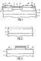
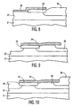
- the AlN layer 3 is masked with a layer of Si 3 N 4 and subsequent etching is carried out to provide a vertical wall gate dielectric 13.
- a reactive ion etching technique will form the vertical walls although a wet etch could be used at the expense of an undercut under the gate dielectric 13.
- the p-type layer 2 of GaN is etched down to the line 10 in order to provide a subsequent underetch 11 of the layer 2 of GaN beneath the gate dielectric 13, as shown in Figure 4.
Landscapes
- Engineering & Computer Science (AREA)
- Physics & Mathematics (AREA)
- Condensed Matter Physics & Semiconductors (AREA)
- General Physics & Mathematics (AREA)
- Manufacturing & Machinery (AREA)
- Computer Hardware Design (AREA)
- Microelectronics & Electronic Packaging (AREA)
- Power Engineering (AREA)
- Thin Film Transistor (AREA)
- Insulated Gate Type Field-Effect Transistor (AREA)
- Formation Of Insulating Films (AREA)
Applications Claiming Priority (3)
| Application Number | Priority Date | Filing Date | Title |
|---|---|---|---|
| US08/583,148 US5915164A (en) | 1995-12-28 | 1995-12-28 | Methods of making high voltage GaN-A1N based semiconductor devices |
| US583148 | 1995-12-28 | ||
| PCT/IB1996/001377 WO1997024752A2 (en) | 1995-12-28 | 1996-12-06 | A METHOD OF MANUFACTURING A HIGH VOLTAGE GaN-AlN BASED SEMICONDUCTOR DEVICE AND SEMICONDUCTOR DEVICE MADE |
Publications (2)
| Publication Number | Publication Date |
|---|---|
| EP0812468A2 EP0812468A2 (en) | 1997-12-17 |
| EP0812468B1 true EP0812468B1 (en) | 2002-11-27 |
Family
ID=24331868
Family Applications (1)
| Application Number | Title | Priority Date | Filing Date |
|---|---|---|---|
| EP96939258A Expired - Lifetime EP0812468B1 (en) | 1995-12-28 | 1996-12-06 | A METHOD OF MANUFACTURING A HIGH VOLTAGE GaN-AlN BASED SEMICONDUCTOR DEVICE AND SEMICONDUCTOR DEVICE MADE |
Country Status (5)
| Country | Link |
|---|---|
| US (2) | US5915164A (enExample) |
| EP (1) | EP0812468B1 (enExample) |
| JP (1) | JPH11501463A (enExample) |
| DE (1) | DE69625045T2 (enExample) |
| WO (1) | WO1997024752A2 (enExample) |
Cited By (2)
| Publication number | Priority date | Publication date | Assignee | Title |
|---|---|---|---|---|
| US8975664B2 (en) | 2012-06-27 | 2015-03-10 | Triquint Semiconductor, Inc. | Group III-nitride transistor using a regrown structure |
| US9054167B2 (en) | 2011-10-26 | 2015-06-09 | Triquint Semiconductor, Inc. | High electron mobility transistor structure and method |
Families Citing this family (79)
| Publication number | Priority date | Publication date | Assignee | Title |
|---|---|---|---|---|
| US5915164A (en) * | 1995-12-28 | 1999-06-22 | U.S. Philips Corporation | Methods of making high voltage GaN-A1N based semiconductor devices |
| US6031263A (en) * | 1997-07-29 | 2000-02-29 | Micron Technology, Inc. | DEAPROM and transistor with gallium nitride or gallium aluminum nitride gate |
| US6965123B1 (en) | 1997-07-29 | 2005-11-15 | Micron Technology, Inc. | Transistor with variable electron affinity gate and methods of fabrication and use |
| US6746893B1 (en) | 1997-07-29 | 2004-06-08 | Micron Technology, Inc. | Transistor with variable electron affinity gate and methods of fabrication and use |
| US7196929B1 (en) | 1997-07-29 | 2007-03-27 | Micron Technology Inc | Method for operating a memory device having an amorphous silicon carbide gate insulator |
| US7154153B1 (en) * | 1997-07-29 | 2006-12-26 | Micron Technology, Inc. | Memory device |
| US6936849B1 (en) | 1997-07-29 | 2005-08-30 | Micron Technology, Inc. | Silicon carbide gate transistor |
| US6297538B1 (en) * | 1998-03-23 | 2001-10-02 | The University Of Delaware | Metal-insulator-semiconductor field effect transistor having an oxidized aluminum nitride gate insulator formed on a gallium nitride or silicon substrate |
| US6495409B1 (en) * | 1999-01-26 | 2002-12-17 | Agere Systems Inc. | MOS transistor having aluminum nitride gate structure and method of manufacturing same |
| US6093952A (en) * | 1999-03-31 | 2000-07-25 | California Institute Of Technology | Higher power gallium nitride schottky rectifier |
| TW474024B (en) * | 1999-08-16 | 2002-01-21 | Cornell Res Foundation Inc | Passivation of GaN based FETs |
| US6265322B1 (en) | 1999-09-21 | 2001-07-24 | Agere Systems Guardian Corp. | Selective growth process for group III-nitride-based semiconductors |
| DE10004394A1 (de) * | 2000-02-02 | 2001-08-16 | Infineon Technologies Ag | Verfahren zur Grabenätzung in Halbleitermaterial |
| JP4667556B2 (ja) * | 2000-02-18 | 2011-04-13 | 古河電気工業株式会社 | 縦型GaN系電界効果トランジスタ、バイポーラトランジスタと縦型GaN系電界効果トランジスタの製造方法 |
| JP2001267555A (ja) | 2000-03-22 | 2001-09-28 | Matsushita Electric Ind Co Ltd | 半導体装置及びその製造方法 |
| US6690042B2 (en) * | 2000-09-27 | 2004-02-10 | Sensor Electronic Technology, Inc. | Metal oxide semiconductor heterostructure field effect transistor |
| US6593193B2 (en) | 2001-02-27 | 2003-07-15 | Matsushita Electric Industrial Co., Ltd. | Semiconductor device and method for fabricating the same |
| DE10120877A1 (de) * | 2001-04-27 | 2002-10-31 | Philips Corp Intellectual Pty | Anordnung mit einem Halbleiterbauelement |
| US20040029365A1 (en) * | 2001-05-07 | 2004-02-12 | Linthicum Kevin J. | Methods of fabricating gallium nitride microelectronic layers on silicon layers and gallium nitride microelectronic structures formed thereby |
| JP3866540B2 (ja) * | 2001-07-06 | 2007-01-10 | 株式会社東芝 | 窒化物半導体素子およびその製造方法 |
| US7030428B2 (en) * | 2001-12-03 | 2006-04-18 | Cree, Inc. | Strain balanced nitride heterojunction transistors |
| JP4104891B2 (ja) * | 2002-04-01 | 2008-06-18 | 三菱電機株式会社 | 半導体装置の製造方法 |
| US7473947B2 (en) * | 2002-07-12 | 2009-01-06 | Intel Corporation | Process for ultra-thin body SOI devices that incorporate EPI silicon tips and article made thereby |
| US6830945B2 (en) * | 2002-09-16 | 2004-12-14 | Hrl Laboratories, Llc | Method for fabricating a non-planar nitride-based heterostructure field effect transistor |
| WO2004025733A1 (en) * | 2002-09-16 | 2004-03-25 | Hrl Laboratories, Llc | Non-planar nitride-based semiconductor structure and metehod for fabricating the same |
| US6986693B2 (en) * | 2003-03-26 | 2006-01-17 | Lucent Technologies Inc. | Group III-nitride layers with patterned surfaces |
| US6847057B1 (en) * | 2003-08-01 | 2005-01-25 | Lumileds Lighting U.S., Llc | Semiconductor light emitting devices |
| US20050040212A1 (en) * | 2003-08-23 | 2005-02-24 | Kuang-Neng Yang | Method for manufacturing nitride light-emitting device |
| US7071498B2 (en) * | 2003-12-17 | 2006-07-04 | Nitronex Corporation | Gallium nitride material devices including an electrode-defining layer and methods of forming the same |
| KR20050065716A (ko) * | 2003-12-23 | 2005-06-30 | 삼성전자주식회사 | 강유전성 액정 소자의 배향 방법 및 배향 장치 |
| US7045404B2 (en) * | 2004-01-16 | 2006-05-16 | Cree, Inc. | Nitride-based transistors with a protective layer and a low-damage recess and methods of fabrication thereof |
| US7901994B2 (en) * | 2004-01-16 | 2011-03-08 | Cree, Inc. | Methods of manufacturing group III nitride semiconductor devices with silicon nitride layers |
| US7170111B2 (en) * | 2004-02-05 | 2007-01-30 | Cree, Inc. | Nitride heterojunction transistors having charge-transfer induced energy barriers and methods of fabricating the same |
| US7612390B2 (en) | 2004-02-05 | 2009-11-03 | Cree, Inc. | Heterojunction transistors including energy barriers |
| US7432142B2 (en) * | 2004-05-20 | 2008-10-07 | Cree, Inc. | Methods of fabricating nitride-based transistors having regrown ohmic contact regions |
| US7084441B2 (en) * | 2004-05-20 | 2006-08-01 | Cree, Inc. | Semiconductor devices having a hybrid channel layer, current aperture transistors and methods of fabricating same |
| KR100609542B1 (ko) * | 2004-06-08 | 2006-08-08 | 주식회사 하이닉스반도체 | 알루미늄 질화막을 게이트 절연막으로 하는 반도체 소자의게이트 전극 제조 방법 |
| US7361946B2 (en) * | 2004-06-28 | 2008-04-22 | Nitronex Corporation | Semiconductor device-based sensors |
| US20060017064A1 (en) * | 2004-07-26 | 2006-01-26 | Saxler Adam W | Nitride-based transistors having laterally grown active region and methods of fabricating same |
| US7709859B2 (en) * | 2004-11-23 | 2010-05-04 | Cree, Inc. | Cap layers including aluminum nitride for nitride-based transistors |
| US7456443B2 (en) * | 2004-11-23 | 2008-11-25 | Cree, Inc. | Transistors having buried n-type and p-type regions beneath the source region |
| US7161194B2 (en) * | 2004-12-06 | 2007-01-09 | Cree, Inc. | High power density and/or linearity transistors |
| US7465967B2 (en) | 2005-03-15 | 2008-12-16 | Cree, Inc. | Group III nitride field effect transistors (FETS) capable of withstanding high temperature reverse bias test conditions |
| US7626217B2 (en) * | 2005-04-11 | 2009-12-01 | Cree, Inc. | Composite substrates of conductive and insulating or semi-insulating group III-nitrides for group III-nitride devices |
| US8575651B2 (en) | 2005-04-11 | 2013-11-05 | Cree, Inc. | Devices having thick semi-insulating epitaxial gallium nitride layer |
| US7544963B2 (en) * | 2005-04-29 | 2009-06-09 | Cree, Inc. | Binary group III-nitride based high electron mobility transistors |
| US7615774B2 (en) * | 2005-04-29 | 2009-11-10 | Cree.Inc. | Aluminum free group III-nitride based high electron mobility transistors |
| US9331192B2 (en) | 2005-06-29 | 2016-05-03 | Cree, Inc. | Low dislocation density group III nitride layers on silicon carbide substrates and methods of making the same |
| US20070018198A1 (en) * | 2005-07-20 | 2007-01-25 | Brandes George R | High electron mobility electronic device structures comprising native substrates and methods for making the same |
| US7994632B2 (en) * | 2006-01-10 | 2011-08-09 | International Rectifier Corporation | Interdigitated conductive lead frame or laminate lead frame for GaN die |
| US7952109B2 (en) * | 2006-07-10 | 2011-05-31 | Alcatel-Lucent Usa Inc. | Light-emitting crystal structures |
| US7266257B1 (en) | 2006-07-12 | 2007-09-04 | Lucent Technologies Inc. | Reducing crosstalk in free-space optical communications |
| US8823057B2 (en) | 2006-11-06 | 2014-09-02 | Cree, Inc. | Semiconductor devices including implanted regions for providing low-resistance contact to buried layers and related devices |
| US8878245B2 (en) * | 2006-11-30 | 2014-11-04 | Cree, Inc. | Transistors and method for making ohmic contact to transistors |
| JP2008159631A (ja) * | 2006-12-20 | 2008-07-10 | Furukawa Electric Co Ltd:The | Iii−v族窒化物化合物半導体電界効果トランジスタおよびその製造方法 |
| JP4653124B2 (ja) * | 2007-01-12 | 2011-03-16 | 古河電気工業株式会社 | 半導体素子製造方法 |
| US9484499B2 (en) * | 2007-04-20 | 2016-11-01 | Cree, Inc. | Transparent ohmic contacts on light emitting diodes with carrier substrates |
| JP2008311392A (ja) * | 2007-06-14 | 2008-12-25 | Furukawa Electric Co Ltd:The | Iii族窒化物半導体を用いた電界効果トランジスタ |
| JP2009076673A (ja) * | 2007-09-20 | 2009-04-09 | Furukawa Electric Co Ltd:The | Iii族窒化物半導体を用いた電界効果トランジスタ |
| JP2009088081A (ja) * | 2007-09-28 | 2009-04-23 | Furukawa Electric Co Ltd:The | Iii族窒化物半導体を用いた電界効果トランジスタ |
| US8368100B2 (en) | 2007-11-14 | 2013-02-05 | Cree, Inc. | Semiconductor light emitting diodes having reflective structures and methods of fabricating same |
| US8304809B2 (en) * | 2007-11-16 | 2012-11-06 | Furukawa Electric Co., Ltd. | GaN-based semiconductor device and method of manufacturing the same |
| JP5463529B2 (ja) * | 2008-06-11 | 2014-04-09 | 古河電気工業株式会社 | 電界効果トランジスタの製造方法 |
| JP5355959B2 (ja) * | 2008-08-08 | 2013-11-27 | 古河電気工業株式会社 | 電界効果トランジスタおよび電界効果トランジスタの製造方法 |
| US8741715B2 (en) * | 2009-04-29 | 2014-06-03 | Cree, Inc. | Gate electrodes for millimeter-wave operation and methods of fabrication |
| WO2010151857A2 (en) * | 2009-06-26 | 2010-12-29 | Cornell University | Method for forming iii-v semiconductor structures including aluminum-silicon nitride passivation |
| US8270131B2 (en) * | 2009-07-31 | 2012-09-18 | Infineon Technologies Ag | Electrostatic discharge protection element and electrostatic discharge protection chip and method of producing the same |
| KR101774933B1 (ko) * | 2010-03-02 | 2017-09-06 | 삼성전자 주식회사 | 듀얼 디플리션을 나타내는 고 전자 이동도 트랜지스터 및 그 제조방법 |
| US20130099284A1 (en) * | 2011-10-20 | 2013-04-25 | Triquint Semiconductor, Inc. | Group iii-nitride metal-insulator-semiconductor heterostructure field-effect transistors |
| JP5306438B2 (ja) * | 2011-11-14 | 2013-10-02 | シャープ株式会社 | 電界効果トランジスタおよびその製造方法 |
| JP6150322B2 (ja) * | 2012-08-03 | 2017-06-21 | ローム株式会社 | 窒化物半導体素子 |
| US9123533B2 (en) * | 2012-08-10 | 2015-09-01 | Avogy, Inc. | Method and system for in-situ etch and regrowth in gallium nitride based devices |
| US9099490B2 (en) | 2012-09-28 | 2015-08-04 | Intel Corporation | Self-aligned structures and methods for asymmetric GaN transistors and enhancement mode operation |
| US9552979B2 (en) * | 2013-05-31 | 2017-01-24 | Asm Ip Holding B.V. | Cyclic aluminum nitride deposition in a batch reactor |
| US9093532B2 (en) | 2013-06-21 | 2015-07-28 | International Business Machines Corporation | Overlapped III-V finFET with doped semiconductor extensions |
| USD826871S1 (en) | 2014-12-11 | 2018-08-28 | Cree, Inc. | Light emitting diode device |
| CN112242441A (zh) * | 2019-07-16 | 2021-01-19 | 联华电子股份有限公司 | 高电子迁移率晶体管 |
| DE102020004758A1 (de) * | 2019-08-30 | 2021-03-04 | Semiconductor Components Industries, Llc | Siliciumcarbid-feldeffekttransistoren |
| JP7767762B2 (ja) * | 2021-08-16 | 2025-11-12 | 住友電気工業株式会社 | 半導体装置及び半導体装置の製造方法 |
Family Cites Families (12)
| Publication number | Priority date | Publication date | Assignee | Title |
|---|---|---|---|---|
| NL8701497A (nl) * | 1987-06-26 | 1989-01-16 | Philips Nv | Halfgeleiderinrichting voor het opwekken van electromagnetische straling. |
| JP3026087B2 (ja) * | 1989-03-01 | 2000-03-27 | 豊田合成株式会社 | 窒化ガリウム系化合物半導体の気相成長方法 |
| US5210051A (en) * | 1990-03-27 | 1993-05-11 | Cree Research, Inc. | High efficiency light emitting diodes from bipolar gallium nitride |
| JP3078821B2 (ja) * | 1990-05-30 | 2000-08-21 | 豊田合成株式会社 | 半導体のドライエッチング方法 |
| US5192987A (en) * | 1991-05-17 | 1993-03-09 | Apa Optics, Inc. | High electron mobility transistor with GaN/Alx Ga1-x N heterojunctions |
| JP2666228B2 (ja) * | 1991-10-30 | 1997-10-22 | 豊田合成株式会社 | 窒化ガリウム系化合物半導体発光素子 |
| DE4323814A1 (de) * | 1992-09-25 | 1994-03-31 | Siemens Ag | MIS-Feldeffekttransistor |
| US5393993A (en) * | 1993-12-13 | 1995-02-28 | Cree Research, Inc. | Buffer structure between silicon carbide and gallium nitride and resulting semiconductor devices |
| JPH07273366A (ja) * | 1994-03-28 | 1995-10-20 | Pioneer Electron Corp | Iii族窒化物発光素子の製造方法 |
| SE9404452D0 (sv) * | 1994-12-22 | 1994-12-22 | Abb Research Ltd | Semiconductor device having an insulated gate |
| US5650361A (en) * | 1995-11-21 | 1997-07-22 | The Aerospace Corporation | Low temperature photolytic deposition of aluminum nitride thin films |
| US5915164A (en) * | 1995-12-28 | 1999-06-22 | U.S. Philips Corporation | Methods of making high voltage GaN-A1N based semiconductor devices |
-
1995
- 1995-12-28 US US08/583,148 patent/US5915164A/en not_active Expired - Fee Related
-
1996
- 1996-12-06 DE DE69625045T patent/DE69625045T2/de not_active Expired - Fee Related
- 1996-12-06 WO PCT/IB1996/001377 patent/WO1997024752A2/en not_active Ceased
- 1996-12-06 EP EP96939258A patent/EP0812468B1/en not_active Expired - Lifetime
- 1996-12-06 JP JP9524138A patent/JPH11501463A/ja not_active Ceased
-
1997
- 1997-11-12 US US08/968,680 patent/US5990531A/en not_active Expired - Fee Related
Non-Patent Citations (1)
| Title |
|---|
| KHAN M.A. ET AL: "Current/voltage characteristic collapse in AlGaN/GaN heterostructure insulated gate field effect transistors at high drain bias", ELECTRONICS LETTERS, vol. 30, no. 25, 8 December 1994 (1994-12-08), pages 2175 - 2176, XP006001452, DOI: doi:10.1049/el:19941461 * |
Cited By (2)
| Publication number | Priority date | Publication date | Assignee | Title |
|---|---|---|---|---|
| US9054167B2 (en) | 2011-10-26 | 2015-06-09 | Triquint Semiconductor, Inc. | High electron mobility transistor structure and method |
| US8975664B2 (en) | 2012-06-27 | 2015-03-10 | Triquint Semiconductor, Inc. | Group III-nitride transistor using a regrown structure |
Also Published As
| Publication number | Publication date |
|---|---|
| JPH11501463A (ja) | 1999-02-02 |
| WO1997024752A3 (en) | 1997-08-28 |
| US5990531A (en) | 1999-11-23 |
| US5915164A (en) | 1999-06-22 |
| DE69625045T2 (de) | 2003-07-24 |
| WO1997024752A2 (en) | 1997-07-10 |
| DE69625045D1 (de) | 2003-01-09 |
| EP0812468A2 (en) | 1997-12-17 |
Similar Documents
| Publication | Publication Date | Title |
|---|---|---|
| EP0812468B1 (en) | A METHOD OF MANUFACTURING A HIGH VOLTAGE GaN-AlN BASED SEMICONDUCTOR DEVICE AND SEMICONDUCTOR DEVICE MADE | |
| US20200343375A1 (en) | Lateral iii-nitride devices including a vertical gate module | |
| Chen et al. | Al x Ga1− x As–GaAs metal–oxide semiconductor field effect transistors formed by lateral water vapor oxidation of AlAs | |
| US7893491B2 (en) | Semiconductor superjunction structure | |
| KR100850026B1 (ko) | Ⅲ-질화물 전류 제어 디바이스와 그 제조방법 | |
| US7038253B2 (en) | GaN-based field effect transistor of a normally-off type | |
| US6100549A (en) | High breakdown voltage resurf HFET | |
| US5591655A (en) | Process for manufacturing a vertical switched-emitter structure with improved lateral isolation | |
| US8829574B2 (en) | Method and system for a GaN vertical JFET with self-aligned source and gate | |
| US20090321854A1 (en) | Mis field effect transistor and method for manufacturing the same | |
| US7629616B2 (en) | Silicon carbide self-aligned epitaxial MOSFET for high powered device applications | |
| US5661312A (en) | Silicon carbide MOSFET | |
| KR100883795B1 (ko) | 대칭적인 트렌치 mosfet 디바이스 및 그 제조 방법 | |
| US20080203471A1 (en) | Nitride semiconductor device and method for producing nitride semiconductor device | |
| US20240355925A1 (en) | Gate-source structure and manufacturing method thereof, and asymmetric trench mosfet and manufacturing method thereof | |
| US7601568B2 (en) | MOS transistor and method for producing a MOS transistor structure | |
| US10991820B2 (en) | Manufacturing method for forming insulating structure of high electron mobility transistor | |
| US20150132900A1 (en) | VERTICAL GaN JFET WITH LOW GATE-DRAIN CAPACITANCE AND HIGH GATE-SOURCE CAPACITANCE | |
| KR20100051240A (ko) | 질화물계 이종접합 전계효과 트랜지스터 | |
| CN105655388A (zh) | 一种GaN基P型栅极增强型HEMT器件及其制备方法 | |
| WO2017196835A1 (en) | Heterojunction schottky gate bipolar transistor | |
| US20040104384A1 (en) | Growth of high temperature, high power, high speed electronics | |
| TWI835394B (zh) | 半導體元件 | |
| KR20250002978A (ko) | 반도체 소자 및 이의 제조 방법 | |
| KR940003096A (ko) | 고전자 이동도 트랜지스터 및 그의 제조방법 |
Legal Events
| Date | Code | Title | Description |
|---|---|---|---|
| PUAI | Public reference made under article 153(3) epc to a published international application that has entered the european phase |
Free format text: ORIGINAL CODE: 0009012 |
|
| AK | Designated contracting states |
Kind code of ref document: A2 Designated state(s): DE FR GB NL |
|
| 17P | Request for examination filed |
Effective date: 19980112 |
|
| 17Q | First examination report despatched |
Effective date: 20010423 |
|
| GRAG | Despatch of communication of intention to grant |
Free format text: ORIGINAL CODE: EPIDOS AGRA |
|
| GRAG | Despatch of communication of intention to grant |
Free format text: ORIGINAL CODE: EPIDOS AGRA |
|
| GRAH | Despatch of communication of intention to grant a patent |
Free format text: ORIGINAL CODE: EPIDOS IGRA |
|
| GRAH | Despatch of communication of intention to grant a patent |
Free format text: ORIGINAL CODE: EPIDOS IGRA |
|
| GRAA | (expected) grant |
Free format text: ORIGINAL CODE: 0009210 |
|
| AK | Designated contracting states |
Kind code of ref document: B1 Designated state(s): DE FR GB NL |
|
| PG25 | Lapsed in a contracting state [announced via postgrant information from national office to epo] |
Ref country code: NL Free format text: LAPSE BECAUSE OF FAILURE TO SUBMIT A TRANSLATION OF THE DESCRIPTION OR TO PAY THE FEE WITHIN THE PRESCRIBED TIME-LIMIT Effective date: 20021127 |
|
| REG | Reference to a national code |
Ref country code: GB Ref legal event code: FG4D |
|
| REF | Corresponds to: |
Ref document number: 69625045 Country of ref document: DE Date of ref document: 20030109 |
|
| REG | Reference to a national code |
Ref country code: GB Ref legal event code: 746 Effective date: 20030305 |
|
| NLV1 | Nl: lapsed or annulled due to failure to fulfill the requirements of art. 29p and 29m of the patents act | ||
| ET | Fr: translation filed | ||
| REG | Reference to a national code |
Ref country code: FR Ref legal event code: D6 |
|
| PLBE | No opposition filed within time limit |
Free format text: ORIGINAL CODE: 0009261 |
|
| STAA | Information on the status of an ep patent application or granted ep patent |
Free format text: STATUS: NO OPPOSITION FILED WITHIN TIME LIMIT |
|
| 26N | No opposition filed |
Effective date: 20030828 |
|
| PGFP | Annual fee paid to national office [announced via postgrant information from national office to epo] |
Ref country code: GB Payment date: 20061218 Year of fee payment: 11 |
|
| PGFP | Annual fee paid to national office [announced via postgrant information from national office to epo] |
Ref country code: DE Payment date: 20070208 Year of fee payment: 11 |
|
| PGFP | Annual fee paid to national office [announced via postgrant information from national office to epo] |
Ref country code: FR Payment date: 20061227 Year of fee payment: 11 |
|
| GBPC | Gb: european patent ceased through non-payment of renewal fee |
Effective date: 20071206 |
|
| PG25 | Lapsed in a contracting state [announced via postgrant information from national office to epo] |
Ref country code: DE Free format text: LAPSE BECAUSE OF NON-PAYMENT OF DUE FEES Effective date: 20080701 |
|
| REG | Reference to a national code |
Ref country code: FR Ref legal event code: ST Effective date: 20081020 |
|
| PG25 | Lapsed in a contracting state [announced via postgrant information from national office to epo] |
Ref country code: GB Free format text: LAPSE BECAUSE OF NON-PAYMENT OF DUE FEES Effective date: 20071206 |
|
| PG25 | Lapsed in a contracting state [announced via postgrant information from national office to epo] |
Ref country code: FR Free format text: LAPSE BECAUSE OF NON-PAYMENT OF DUE FEES Effective date: 20071231 |