US9093532B2 - Overlapped III-V finFET with doped semiconductor extensions - Google Patents
Overlapped III-V finFET with doped semiconductor extensions Download PDFInfo
- Publication number
- US9093532B2 US9093532B2 US13/923,629 US201313923629A US9093532B2 US 9093532 B2 US9093532 B2 US 9093532B2 US 201313923629 A US201313923629 A US 201313923629A US 9093532 B2 US9093532 B2 US 9093532B2
- Authority
- US
- United States
- Prior art keywords
- semiconductor
- iii
- gate
- fin
- gate structure
- Prior art date
- Legal status (The legal status is an assumption and is not a legal conclusion. Google has not performed a legal analysis and makes no representation as to the accuracy of the status listed.)
- Active, expires
Links
- 239000004065 semiconductor Substances 0.000 title claims abstract description 338
- 239000000463 material Substances 0.000 claims abstract description 198
- 150000001875 compounds Chemical class 0.000 claims abstract description 108
- 125000006850 spacer group Chemical group 0.000 claims abstract description 43
- 229910052710 silicon Inorganic materials 0.000 claims abstract description 9
- 239000010703 silicon Substances 0.000 claims abstract description 9
- 239000003989 dielectric material Substances 0.000 claims description 50
- 239000004020 conductor Substances 0.000 claims description 21
- 239000012212 insulator Substances 0.000 claims description 21
- 239000002019 doping agent Substances 0.000 claims description 13
- 238000000034 method Methods 0.000 description 27
- 238000005530 etching Methods 0.000 description 18
- 239000000758 substrate Substances 0.000 description 18
- 238000000623 plasma-assisted chemical vapour deposition Methods 0.000 description 12
- 238000005229 chemical vapour deposition Methods 0.000 description 11
- 230000015572 biosynthetic process Effects 0.000 description 10
- 229920002120 photoresistant polymer Polymers 0.000 description 9
- VYPSYNLAJGMNEJ-UHFFFAOYSA-N Silicium dioxide Chemical compound O=[Si]=O VYPSYNLAJGMNEJ-UHFFFAOYSA-N 0.000 description 8
- 238000000151 deposition Methods 0.000 description 8
- 238000005137 deposition process Methods 0.000 description 8
- XUIMIQQOPSSXEZ-UHFFFAOYSA-N Silicon Chemical compound [Si] XUIMIQQOPSSXEZ-UHFFFAOYSA-N 0.000 description 7
- KWYUFKZDYYNOTN-UHFFFAOYSA-M Potassium hydroxide Chemical compound [OH-].[K+] KWYUFKZDYYNOTN-UHFFFAOYSA-M 0.000 description 6
- 230000008021 deposition Effects 0.000 description 6
- 229910052751 metal Inorganic materials 0.000 description 6
- 239000002184 metal Substances 0.000 description 6
- 238000005240 physical vapour deposition Methods 0.000 description 6
- 238000001459 lithography Methods 0.000 description 5
- 229910052814 silicon oxide Inorganic materials 0.000 description 5
- 229910000530 Gallium indium arsenide Inorganic materials 0.000 description 4
- GPXJNWSHGFTCBW-UHFFFAOYSA-N Indium phosphide Chemical compound [In]#P GPXJNWSHGFTCBW-UHFFFAOYSA-N 0.000 description 4
- KXNLCSXBJCPWGL-UHFFFAOYSA-N [Ga].[As].[In] Chemical compound [Ga].[As].[In] KXNLCSXBJCPWGL-UHFFFAOYSA-N 0.000 description 4
- 229910045601 alloy Inorganic materials 0.000 description 4
- 239000000956 alloy Substances 0.000 description 4
- 230000005669 field effect Effects 0.000 description 4
- 230000000737 periodic effect Effects 0.000 description 4
- 239000002243 precursor Substances 0.000 description 4
- 239000000126 substance Substances 0.000 description 4
- 229910052721 tungsten Inorganic materials 0.000 description 4
- -1 HfOxNy Inorganic materials 0.000 description 3
- 229910052782 aluminium Inorganic materials 0.000 description 3
- 238000000231 atomic layer deposition Methods 0.000 description 3
- 238000005516 engineering process Methods 0.000 description 3
- JBRZTFJDHDCESZ-UHFFFAOYSA-N AsGa Chemical compound [As]#[Ga] JBRZTFJDHDCESZ-UHFFFAOYSA-N 0.000 description 2
- PXHVJJICTQNCMI-UHFFFAOYSA-N Nickel Chemical compound [Ni] PXHVJJICTQNCMI-UHFFFAOYSA-N 0.000 description 2
- KDLHZDBZIXYQEI-UHFFFAOYSA-N Palladium Chemical compound [Pd] KDLHZDBZIXYQEI-UHFFFAOYSA-N 0.000 description 2
- 229910052581 Si3N4 Inorganic materials 0.000 description 2
- GWEVSGVZZGPLCZ-UHFFFAOYSA-N Titan oxide Chemical compound O=[Ti]=O GWEVSGVZZGPLCZ-UHFFFAOYSA-N 0.000 description 2
- MCMNRKCIXSYSNV-UHFFFAOYSA-N Zirconium dioxide Chemical compound O=[Zr]=O MCMNRKCIXSYSNV-UHFFFAOYSA-N 0.000 description 2
- 239000005380 borophosphosilicate glass Substances 0.000 description 2
- 239000013078 crystal Substances 0.000 description 2
- 239000011521 glass Substances 0.000 description 2
- 238000005468 ion implantation Methods 0.000 description 2
- 150000002500 ions Chemical class 0.000 description 2
- 150000004767 nitrides Chemical class 0.000 description 2
- 238000001020 plasma etching Methods 0.000 description 2
- BASFCYQUMIYNBI-UHFFFAOYSA-N platinum Chemical compound [Pt] BASFCYQUMIYNBI-UHFFFAOYSA-N 0.000 description 2
- 229910021332 silicide Inorganic materials 0.000 description 2
- FVBUAEGBCNSCDD-UHFFFAOYSA-N silicide(4-) Chemical compound [Si-4] FVBUAEGBCNSCDD-UHFFFAOYSA-N 0.000 description 2
- 239000000377 silicon dioxide Substances 0.000 description 2
- 235000012239 silicon dioxide Nutrition 0.000 description 2
- HQVNEWCFYHHQES-UHFFFAOYSA-N silicon nitride Chemical compound N12[Si]34N5[Si]62N3[Si]51N64 HQVNEWCFYHHQES-UHFFFAOYSA-N 0.000 description 2
- 238000004544 sputter deposition Methods 0.000 description 2
- 239000010937 tungsten Substances 0.000 description 2
- 229910002244 LaAlO3 Inorganic materials 0.000 description 1
- BPQQTUXANYXVAA-UHFFFAOYSA-N Orthosilicate Chemical compound [O-][Si]([O-])([O-])[O-] BPQQTUXANYXVAA-UHFFFAOYSA-N 0.000 description 1
- KJTLSVCANCCWHF-UHFFFAOYSA-N Ruthenium Chemical compound [Ru] KJTLSVCANCCWHF-UHFFFAOYSA-N 0.000 description 1
- 229910004205 SiNX Inorganic materials 0.000 description 1
- 229910002370 SrTiO3 Inorganic materials 0.000 description 1
- 229910010303 TiOxNy Inorganic materials 0.000 description 1
- RTAQQCXQSZGOHL-UHFFFAOYSA-N Titanium Chemical compound [Ti] RTAQQCXQSZGOHL-UHFFFAOYSA-N 0.000 description 1
- NRTOMJZYCJJWKI-UHFFFAOYSA-N Titanium nitride Chemical compound [Ti]#N NRTOMJZYCJJWKI-UHFFFAOYSA-N 0.000 description 1
- 229910003134 ZrOx Inorganic materials 0.000 description 1
- XAGFODPZIPBFFR-UHFFFAOYSA-N aluminium Chemical compound [Al] XAGFODPZIPBFFR-UHFFFAOYSA-N 0.000 description 1
- PNEYBMLMFCGWSK-UHFFFAOYSA-N aluminium oxide Inorganic materials [O-2].[O-2].[O-2].[Al+3].[Al+3] PNEYBMLMFCGWSK-UHFFFAOYSA-N 0.000 description 1
- RNQKDQAVIXDKAG-UHFFFAOYSA-N aluminum gallium Chemical compound [Al].[Ga] RNQKDQAVIXDKAG-UHFFFAOYSA-N 0.000 description 1
- 238000004380 ashing Methods 0.000 description 1
- 239000000969 carrier Substances 0.000 description 1
- 239000011248 coating agent Substances 0.000 description 1
- 238000000576 coating method Methods 0.000 description 1
- 238000010276 construction Methods 0.000 description 1
- 229910052802 copper Inorganic materials 0.000 description 1
- PMHQVHHXPFUNSP-UHFFFAOYSA-M copper(1+);methylsulfanylmethane;bromide Chemical compound Br[Cu].CSC PMHQVHHXPFUNSP-UHFFFAOYSA-M 0.000 description 1
- 229910052593 corundum Inorganic materials 0.000 description 1
- 238000009792 diffusion process Methods 0.000 description 1
- 238000010494 dissociation reaction Methods 0.000 description 1
- 230000005593 dissociations Effects 0.000 description 1
- 230000008020 evaporation Effects 0.000 description 1
- 238000001704 evaporation Methods 0.000 description 1
- 229940104869 fluorosilicate Drugs 0.000 description 1
- CJNBYAVZURUTKZ-UHFFFAOYSA-N hafnium(IV) oxide Inorganic materials O=[Hf]=O CJNBYAVZURUTKZ-UHFFFAOYSA-N 0.000 description 1
- 238000004050 hot filament vapor deposition Methods 0.000 description 1
- 238000011065 in-situ storage Methods 0.000 description 1
- 239000011810 insulating material Substances 0.000 description 1
- 238000010884 ion-beam technique Methods 0.000 description 1
- MRELNEQAGSRDBK-UHFFFAOYSA-N lanthanum oxide Inorganic materials [O-2].[O-2].[O-2].[La+3].[La+3] MRELNEQAGSRDBK-UHFFFAOYSA-N 0.000 description 1
- 238000000608 laser ablation Methods 0.000 description 1
- 239000007769 metal material Substances 0.000 description 1
- 150000002739 metals Chemical class 0.000 description 1
- 239000000203 mixture Substances 0.000 description 1
- 229910052759 nickel Inorganic materials 0.000 description 1
- RUFLMLWJRZAWLJ-UHFFFAOYSA-N nickel silicide Chemical compound [Ni]=[Si]=[Ni] RUFLMLWJRZAWLJ-UHFFFAOYSA-N 0.000 description 1
- 229910021334 nickel silicide Inorganic materials 0.000 description 1
- 230000003647 oxidation Effects 0.000 description 1
- 238000007254 oxidation reaction Methods 0.000 description 1
- TWNQGVIAIRXVLR-UHFFFAOYSA-N oxo(oxoalumanyloxy)alumane Chemical compound O=[Al]O[Al]=O TWNQGVIAIRXVLR-UHFFFAOYSA-N 0.000 description 1
- KTUFCUMIWABKDW-UHFFFAOYSA-N oxo(oxolanthaniooxy)lanthanum Chemical compound O=[La]O[La]=O KTUFCUMIWABKDW-UHFFFAOYSA-N 0.000 description 1
- 229910052763 palladium Inorganic materials 0.000 description 1
- 229910052697 platinum Inorganic materials 0.000 description 1
- 229910021420 polycrystalline silicon Inorganic materials 0.000 description 1
- 229920005591 polysilicon Polymers 0.000 description 1
- 230000005855 radiation Effects 0.000 description 1
- 229910052707 ruthenium Inorganic materials 0.000 description 1
- 239000005368 silicate glass Substances 0.000 description 1
- 230000001629 suppression Effects 0.000 description 1
- 229910052715 tantalum Inorganic materials 0.000 description 1
- GUVRBAGPIYLISA-UHFFFAOYSA-N tantalum atom Chemical compound [Ta] GUVRBAGPIYLISA-UHFFFAOYSA-N 0.000 description 1
- 229910052719 titanium Inorganic materials 0.000 description 1
- 239000010936 titanium Substances 0.000 description 1
- 229910021341 titanium silicide Inorganic materials 0.000 description 1
- WFKWXMTUELFFGS-UHFFFAOYSA-N tungsten Chemical compound [W] WFKWXMTUELFFGS-UHFFFAOYSA-N 0.000 description 1
- WQJQOUPTWCFRMM-UHFFFAOYSA-N tungsten disilicide Chemical compound [Si]#[W]#[Si] WQJQOUPTWCFRMM-UHFFFAOYSA-N 0.000 description 1
- 229910021342 tungsten silicide Inorganic materials 0.000 description 1
- 238000001039 wet etching Methods 0.000 description 1
- 229910001845 yogo sapphire Inorganic materials 0.000 description 1
- RUDFQVOCFDJEEF-UHFFFAOYSA-N yttrium(III) oxide Inorganic materials [O-2].[O-2].[O-2].[Y+3].[Y+3] RUDFQVOCFDJEEF-UHFFFAOYSA-N 0.000 description 1
Images


Classifications
-
- H—ELECTRICITY
- H01—ELECTRIC ELEMENTS
- H01L—SEMICONDUCTOR DEVICES NOT COVERED BY CLASS H10
- H01L29/00—Semiconductor devices specially adapted for rectifying, amplifying, oscillating or switching and having potential barriers; Capacitors or resistors having potential barriers, e.g. a PN-junction depletion layer or carrier concentration layer; Details of semiconductor bodies or of electrodes thereof ; Multistep manufacturing processes therefor
- H01L29/66—Types of semiconductor device ; Multistep manufacturing processes therefor
- H01L29/68—Types of semiconductor device ; Multistep manufacturing processes therefor controllable by only the electric current supplied, or only the electric potential applied, to an electrode which does not carry the current to be rectified, amplified or switched
- H01L29/76—Unipolar devices, e.g. field effect transistors
- H01L29/772—Field effect transistors
- H01L29/78—Field effect transistors with field effect produced by an insulated gate
- H01L29/785—Field effect transistors with field effect produced by an insulated gate having a channel with a horizontal current flow in a vertical sidewall of a semiconductor body, e.g. FinFET, MuGFET
-
- H—ELECTRICITY
- H01—ELECTRIC ELEMENTS
- H01L—SEMICONDUCTOR DEVICES NOT COVERED BY CLASS H10
- H01L21/00—Processes or apparatus adapted for the manufacture or treatment of semiconductor or solid state devices or of parts thereof
- H01L21/70—Manufacture or treatment of devices consisting of a plurality of solid state components formed in or on a common substrate or of parts thereof; Manufacture of integrated circuit devices or of parts thereof
- H01L21/77—Manufacture or treatment of devices consisting of a plurality of solid state components or integrated circuits formed in, or on, a common substrate
- H01L21/78—Manufacture or treatment of devices consisting of a plurality of solid state components or integrated circuits formed in, or on, a common substrate with subsequent division of the substrate into plural individual devices
- H01L21/82—Manufacture or treatment of devices consisting of a plurality of solid state components or integrated circuits formed in, or on, a common substrate with subsequent division of the substrate into plural individual devices to produce devices, e.g. integrated circuits, each consisting of a plurality of components
- H01L21/84—Manufacture or treatment of devices consisting of a plurality of solid state components or integrated circuits formed in, or on, a common substrate with subsequent division of the substrate into plural individual devices to produce devices, e.g. integrated circuits, each consisting of a plurality of components the substrate being other than a semiconductor body, e.g. being an insulating body
- H01L21/845—Manufacture or treatment of devices consisting of a plurality of solid state components or integrated circuits formed in, or on, a common substrate with subsequent division of the substrate into plural individual devices to produce devices, e.g. integrated circuits, each consisting of a plurality of components the substrate being other than a semiconductor body, e.g. being an insulating body including field-effect transistors with a horizontal current flow in a vertical sidewall of a semiconductor body, e.g. FinFET, MuGFET
-
- H—ELECTRICITY
- H01—ELECTRIC ELEMENTS
- H01L—SEMICONDUCTOR DEVICES NOT COVERED BY CLASS H10
- H01L27/00—Devices consisting of a plurality of semiconductor or other solid-state components formed in or on a common substrate
- H01L27/02—Devices consisting of a plurality of semiconductor or other solid-state components formed in or on a common substrate including semiconductor components specially adapted for rectifying, oscillating, amplifying or switching and having potential barriers; including integrated passive circuit elements having potential barriers
- H01L27/12—Devices consisting of a plurality of semiconductor or other solid-state components formed in or on a common substrate including semiconductor components specially adapted for rectifying, oscillating, amplifying or switching and having potential barriers; including integrated passive circuit elements having potential barriers the substrate being other than a semiconductor body, e.g. an insulating body
- H01L27/1203—Devices consisting of a plurality of semiconductor or other solid-state components formed in or on a common substrate including semiconductor components specially adapted for rectifying, oscillating, amplifying or switching and having potential barriers; including integrated passive circuit elements having potential barriers the substrate being other than a semiconductor body, e.g. an insulating body the substrate comprising an insulating body on a semiconductor body, e.g. SOI
- H01L27/1211—Devices consisting of a plurality of semiconductor or other solid-state components formed in or on a common substrate including semiconductor components specially adapted for rectifying, oscillating, amplifying or switching and having potential barriers; including integrated passive circuit elements having potential barriers the substrate being other than a semiconductor body, e.g. an insulating body the substrate comprising an insulating body on a semiconductor body, e.g. SOI combined with field-effect transistors with a horizontal current flow in a vertical sidewall of a semiconductor body, e.g. FinFET, MuGFET
-
- H—ELECTRICITY
- H01—ELECTRIC ELEMENTS
- H01L—SEMICONDUCTOR DEVICES NOT COVERED BY CLASS H10
- H01L29/00—Semiconductor devices specially adapted for rectifying, amplifying, oscillating or switching and having potential barriers; Capacitors or resistors having potential barriers, e.g. a PN-junction depletion layer or carrier concentration layer; Details of semiconductor bodies or of electrodes thereof ; Multistep manufacturing processes therefor
- H01L29/02—Semiconductor bodies ; Multistep manufacturing processes therefor
- H01L29/12—Semiconductor bodies ; Multistep manufacturing processes therefor characterised by the materials of which they are formed
- H01L29/20—Semiconductor bodies ; Multistep manufacturing processes therefor characterised by the materials of which they are formed including, apart from doping materials or other impurities, only AIIIBV compounds
- H01L29/201—Semiconductor bodies ; Multistep manufacturing processes therefor characterised by the materials of which they are formed including, apart from doping materials or other impurities, only AIIIBV compounds including two or more compounds, e.g. alloys
- H01L29/205—Semiconductor bodies ; Multistep manufacturing processes therefor characterised by the materials of which they are formed including, apart from doping materials or other impurities, only AIIIBV compounds including two or more compounds, e.g. alloys in different semiconductor regions, e.g. heterojunctions
-
- H—ELECTRICITY
- H01—ELECTRIC ELEMENTS
- H01L—SEMICONDUCTOR DEVICES NOT COVERED BY CLASS H10
- H01L29/00—Semiconductor devices specially adapted for rectifying, amplifying, oscillating or switching and having potential barriers; Capacitors or resistors having potential barriers, e.g. a PN-junction depletion layer or carrier concentration layer; Details of semiconductor bodies or of electrodes thereof ; Multistep manufacturing processes therefor
- H01L29/02—Semiconductor bodies ; Multistep manufacturing processes therefor
- H01L29/12—Semiconductor bodies ; Multistep manufacturing processes therefor characterised by the materials of which they are formed
- H01L29/26—Semiconductor bodies ; Multistep manufacturing processes therefor characterised by the materials of which they are formed including, apart from doping materials or other impurities, elements provided for in two or more of the groups H01L29/16, H01L29/18, H01L29/20, H01L29/22, H01L29/24, e.g. alloys
- H01L29/267—Semiconductor bodies ; Multistep manufacturing processes therefor characterised by the materials of which they are formed including, apart from doping materials or other impurities, elements provided for in two or more of the groups H01L29/16, H01L29/18, H01L29/20, H01L29/22, H01L29/24, e.g. alloys in different semiconductor regions, e.g. heterojunctions
-
- H—ELECTRICITY
- H01—ELECTRIC ELEMENTS
- H01L—SEMICONDUCTOR DEVICES NOT COVERED BY CLASS H10
- H01L29/00—Semiconductor devices specially adapted for rectifying, amplifying, oscillating or switching and having potential barriers; Capacitors or resistors having potential barriers, e.g. a PN-junction depletion layer or carrier concentration layer; Details of semiconductor bodies or of electrodes thereof ; Multistep manufacturing processes therefor
- H01L29/66—Types of semiconductor device ; Multistep manufacturing processes therefor
- H01L29/66007—Multistep manufacturing processes
- H01L29/66075—Multistep manufacturing processes of devices having semiconductor bodies comprising group 14 or group 13/15 materials
- H01L29/66227—Multistep manufacturing processes of devices having semiconductor bodies comprising group 14 or group 13/15 materials the devices being controllable only by the electric current supplied or the electric potential applied, to an electrode which does not carry the current to be rectified, amplified or switched, e.g. three-terminal devices
- H01L29/66409—Unipolar field-effect transistors
- H01L29/66477—Unipolar field-effect transistors with an insulated gate, i.e. MISFET
- H01L29/66545—Unipolar field-effect transistors with an insulated gate, i.e. MISFET using a dummy, i.e. replacement gate in a process wherein at least a part of the final gate is self aligned to the dummy gate
-
- H—ELECTRICITY
- H01—ELECTRIC ELEMENTS
- H01L—SEMICONDUCTOR DEVICES NOT COVERED BY CLASS H10
- H01L29/00—Semiconductor devices specially adapted for rectifying, amplifying, oscillating or switching and having potential barriers; Capacitors or resistors having potential barriers, e.g. a PN-junction depletion layer or carrier concentration layer; Details of semiconductor bodies or of electrodes thereof ; Multistep manufacturing processes therefor
- H01L29/66—Types of semiconductor device ; Multistep manufacturing processes therefor
- H01L29/66007—Multistep manufacturing processes
- H01L29/66075—Multistep manufacturing processes of devices having semiconductor bodies comprising group 14 or group 13/15 materials
- H01L29/66227—Multistep manufacturing processes of devices having semiconductor bodies comprising group 14 or group 13/15 materials the devices being controllable only by the electric current supplied or the electric potential applied, to an electrode which does not carry the current to be rectified, amplified or switched, e.g. three-terminal devices
- H01L29/66409—Unipolar field-effect transistors
- H01L29/66477—Unipolar field-effect transistors with an insulated gate, i.e. MISFET
- H01L29/66568—Lateral single gate silicon transistors
- H01L29/66575—Lateral single gate silicon transistors where the source and drain or source and drain extensions are self-aligned to the sides of the gate
-
- H—ELECTRICITY
- H01—ELECTRIC ELEMENTS
- H01L—SEMICONDUCTOR DEVICES NOT COVERED BY CLASS H10
- H01L29/00—Semiconductor devices specially adapted for rectifying, amplifying, oscillating or switching and having potential barriers; Capacitors or resistors having potential barriers, e.g. a PN-junction depletion layer or carrier concentration layer; Details of semiconductor bodies or of electrodes thereof ; Multistep manufacturing processes therefor
- H01L29/66—Types of semiconductor device ; Multistep manufacturing processes therefor
- H01L29/66007—Multistep manufacturing processes
- H01L29/66075—Multistep manufacturing processes of devices having semiconductor bodies comprising group 14 or group 13/15 materials
- H01L29/66227—Multistep manufacturing processes of devices having semiconductor bodies comprising group 14 or group 13/15 materials the devices being controllable only by the electric current supplied or the electric potential applied, to an electrode which does not carry the current to be rectified, amplified or switched, e.g. three-terminal devices
- H01L29/66409—Unipolar field-effect transistors
- H01L29/66477—Unipolar field-effect transistors with an insulated gate, i.e. MISFET
- H01L29/66787—Unipolar field-effect transistors with an insulated gate, i.e. MISFET with a gate at the side of the channel
- H01L29/66795—Unipolar field-effect transistors with an insulated gate, i.e. MISFET with a gate at the side of the channel with a horizontal current flow in a vertical sidewall of a semiconductor body, e.g. FinFET, MuGFET
Definitions
- the present application relates to a semiconductor structure and a method of forming the same. More particularly, the present application relates to a fin field effect transistor (finFET) containing an III-V compound semiconductor fin and an undercut extension region located beneath a dielectric spacer that is present on each vertical sidewall of a functional gate structure and a method of forming the same.
- finFET fin field effect transistor
- Planar field-effect transistor (FET) devices which have been widely used in integrated circuits for the past several decades, have been found to be increasingly inefficient on the nanometer scale. Reducing the size of the channel between the terminals of planar transistors to this scale leads to an inefficient leakage of current in the off-state of the transistor, resulting in an increase in power consumption in its idle state.
- FET field-effect transistor
- Multi-gate field-effect transistors have been developed to address this problem, as such transistors incorporate several gates that surround the channel between a source and drain terminal of the transistor on a plurality of surfaces, thereby enabling the suppression of leakage current in the off-state.
- multi-gate devices include several thin fin, which can be made of silicon, that provides the channel between a source and a drain. The fin can be overlaid with one or more pairs of gates, where the gates in a pair are on opposing sides of the fin.
- a semiconductor structure in one aspect of the present application, includes a semiconductor fin comprising an III-V compound semiconductor material located on a surface of an insulator layer.
- the semiconductor structure of the present application further includes a functional gate structure orientated perpendicular to and straddling a portion of the semiconductor fin, wherein a semiconductor channel material having an electron mobility greater than silicon and comprising a different semiconductor material than the semiconductor fin is located beneath the functional gate structure.
- the semiconductor channel material is present on at least each vertical sidewall of the semiconductor fin.
- the semiconductor structure of the present application also includes a dielectric spacer located on each vertical sidewall surface of the functional gate structure.
- the semiconductor structure of the present application yet further includes a doped semiconductor material having a higher dopant content than both the semiconductor fin and the semiconductor channel material located on each side of the functional gate structure and underneath each dielectric spacer, wherein a portion of the doped semiconductor material located beneath each dielectric spacer directly contacts a sidewall surface of semiconductor channel material located on each vertical sidewall of the semiconductor fin.
- a method of forming a semiconductor structure includes forming a semiconductor fin comprising an III-V compound semiconductor material on a surface of an insulator layer.
- a semiconductor channel material is epitaxially grown on exposed surfaces of the semiconductor fin.
- the semiconductor channel material that is grown has an electron mobility greater than silicon and comprises a different semiconductor material than the semiconductor fin.
- a gate structure is formed straddling a portion of the semiconductor fin, wherein the gate structure is orientated perpendicular to the semiconductor fin and wherein a dielectric spacer is present on each vertical sidewall of the gate structure.
- Portions of the semiconductor channel material are selectively etched from atop the structure not protected by the gate structure and from beneath each dielectric spacer, wherein an undercut is provided beneath each dielectric spacer.
- a doped semiconductor material having a higher doped content than both the semiconductor fin and the semiconductor channel material is epitaxially grown on surfaces of the semiconductor fin not including the dielectric spacer and gate structure and within the undercut region.
- FIG. 1A is a top-down view of a semiconductor-on-insulator (SOI) substrate including, from bottom to top, a handle substrate, an insulator layer and an III-V compound semiconductor layer that can be employed in one embodiment of the present application.
- SOI semiconductor-on-insulator
- FIG. 1B is a vertical cross-sectional view of the semiconductor substrate along the vertical plane A-A′ of FIG. 1A .
- FIG. 2A is a top-down view of the (SOI) substrate shown in FIG. 1A after formation of a semiconductor structure containing a plurality of III-V compound semiconductor fins.
- FIG. 2B is a vertical cross-sectional view of the semiconductor structure along the vertical plane A-A′ of FIG. 2A .
- FIG. 2C is a vertical cross-sectional view of the semiconductor structure along the vertical plane B-B′ of FIG. 2A .
- FIG. 3A is a top-down view of the semiconductor structure shown in FIG. 2A after epitaxially growing a semiconductor channel material on vertical sidewall surfaces and a topmost surface of each III-V compound semiconductor fin.
- FIG. 3B is a vertical cross-sectional view of the semiconductor structure along the vertical plane A-A′ of FIG. 3A .
- FIG. 3C is a vertical cross-sectional view of the semiconductor structure along the vertical plane B-B′ of FIG. 3A .
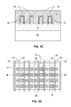
- FIG. 4A is a top-down view of the semiconductor structure shown in FIG. 3A after formation of a plurality of gate structures that are orientated perpendicular to and that straddle each III-V compound semiconductor fin.
- FIG. 4B is a vertical cross-sectional view of the semiconductor structure along the vertical plane A-A′ of FIG. 4A .
- FIG. 4C is a vertical cross-sectional view of the semiconductor structure along the vertical plane B-B′ of FIG. 4A .
- FIG. 5A is a top-down view of the semiconductor structure shown in FIG. 4A after formation of a dielectric spacer on each vertical sidewall surface of each gate structure and straddling each III-V compound semiconductor fin.
- FIG. 5B is a vertical cross-sectional view of the semiconductor structure along the vertical plane A-A′ of FIG. 5A .
- FIG. 5C is a vertical cross-sectional view of the semiconductor structure along the vertical plane B-B′ of FIG. 5A .
- FIG. 5D is a vertical cross-sectional view of the semiconductor structure along the vertical plane C-C′ of FIG. 5A .
- FIG. 6A is a top-down view of the semiconductor structure shown in FIG. 5A after selectively etching portions of the semiconductor channel material from atop the structure not protected by the gate structure and from beneath each dielectric spacer, wherein an undercut is provided beneath each dielectric spacer.
- FIG. 6B is a vertical cross-sectional view of the semiconductor structure along the vertical plane A-A′ of FIG. 6A .
- FIG. 6C is a vertical cross-sectional view of the semiconductor structure along the vertical plane D-D′ of FIG. 6A .
- FIG. 6D is a vertical cross-sectional view of the semiconductor structure along the vertical plane C-C′ of FIG. 6A .
- FIG. 7A is a top-down view of the semiconductor structure shown in FIG. 6A after epitaxially growing a doped semiconductor material on exposed surfaces of each III-V compound semiconductor fin not including the dielectric spacer and gate structures and within the undercut region.
- FIG. 7B is a vertical cross-sectional view of the semiconductor structure along the vertical plane F-F′ of FIG. 7A .
- FIG. 7C is a vertical cross-sectional view of the semiconductor structure along the vertical plane D-D′ of FIG. 7A .
- FIG. 7D is a vertical cross-sectional view of the semiconductor structure along the vertical plane C-C′ of FIG. 7A .
- FIG. 8A is a top-down view of the semiconductor structure shown in FIG. 7A after formation of a dielectric material having a topmost surface that is coplanar with a topmost surface of each gate structure.
- FIG. 8B is a vertical cross-sectional view of the semiconductor structure along the vertical plane F-F′ of FIG. 8A .
- FIG. 8C is a vertical cross-sectional view of the semiconductor structure along the vertical plane D-D′ of FIG. 8A .
- FIG. 8D is a vertical cross-sectional view of the semiconductor structure along the vertical plane C-C′ of FIG. 8A .
- FIG. 9A is a top-down view of the semiconductor structure shown in FIG. 8A after formation of a plurality of via contact structures in the dielectric material which extend from the topmost surface of the dielectric material to an upper surface of a doped semiconductor material portion located on each side of the gate structure.
- FIG. 9B is a vertical cross-sectional view of the semiconductor structure along the vertical plane F-F′ of FIG. 9A .
- FIG. 9C is a vertical cross-sectional view of the semiconductor structure along the vertical plane D-D′ of FIG. 9A .
- FIG. 10A is a top-down view of the semiconductor structure shown in FIG. 8A after removal of the gate structure and replacing the gate structure with a replacement gate structure in accordance with an embodiment of the present application in which the gate structure employed is a sacrificial gate structure.
- FIG. 10B is a vertical cross-sectional view of the semiconductor structure along the vertical plane F-F′ of FIG. 10A .
- FIG. 10C is a vertical cross-sectional view of the semiconductor structure along the vertical plane D-D′ of FIG. 10A .
- FIG. 10D is a vertical cross-sectional view of the semiconductor structure along the vertical plane C-C′ of FIG. 10A .
- the present application which provides a fin field effect transistor (finFET) containing an III-V compound semiconductor fin and an undercut extension region located beneath a dielectric spacer that is present on each vertical sidewall of a functional gate structure and a method of forming the same will now be described in greater detail by referring to the following discussion and drawings that accompany the present application. It is noted that the drawings of the present application are provided for illustrative purposes and, as such, they are not drawn to scale. In the drawings and the description that follows, like elements are referred to by like reference numerals.
- the different vertical cross-sectional views along various planes include: A-A′ which is through a plane in which an III-V compound semiconductor fin will be subsequently formed or is present, B-B′ through a plane perpendicular to each III-V compound semiconductor fin and in which a gate structure will be subsequently formed or is present, C-C′ through a plane perpendicular to each III-V compound semiconductor fin and in which a first doped semiconductor material portion will be formed or is present, D-D′ through a plane perpendicular to each III-V compound semiconductor fin and beneath a dielectric spacer and in which a second doped semiconductor material portion will be formed or is present, F-F′ through a plane in which an III-V compound semiconductor fin is present and in proximity to a vertical sidewall of the III-V compound semiconductor fin. Note the cut F-F′ is approximately 2 nm from the center of each fin which is shown in cut A-
- III-V compound semiconductor device processing requires very low temperatures (on the order of 600° C. or less) to avoid dissociation or damage to the III-V compound semiconductor crystal structure and to the interface between the III-V compound semiconductor material and the overlaying gate dielectric. This makes self-aligned devices very difficult to form since self-aligned devices require some diffusion of dopant to form an extension overlayer. Current solutions require either complex space technology or no spacers whatsoever which is not very robust or manufacturable. In addition, traditional extension doping to create overlap for silicon transistors is through ion implantation, which is not as effective for III-V compound semiconductor materials and can cause crystal damage in the III-V compound semiconductor material.
- the present application overcomes the drawbacks associated with fabricating finFET semiconductor devices including a semiconductor fin comprising an III-V compound semiconductor material by utilizing a selective etch of a semiconductor channel layer and growth of an epitaxially doped semiconductor material under a gate region (functional gate structure or sacrificial gate structure) to force controllable overlap.
- the method of the present application can eliminate ion implantation damage. The method of the present application is now described in greater detail.
- FIGS. 1A and 1B there are illustrated various views of a semiconductor-on-insulator (SOI) substrate that can be employed in one embodiment of the present application.
- SOI substrate that can be employed in the present application includes, from bottom to top, a handle substrate 10 , an insulator layer 12 and an III-V compound semiconductor layer 14 .
- the handle substrate 10 can include a semiconductor material, a conductive material, and/or a dielectric material.
- the handle substrate 10 provides mechanical support to the insulator layer 12 and the III-V compound semiconductor layer 14 .
- the thickness of the handle substrate 10 can be from 30 microns to 2 mm, although lesser and greater thicknesses can also be employed.
- the insulator layer 12 includes an insulator material.
- an insulator material refers to a material having a resistivity greater than 3 ⁇ 10 3 Ohm-cm.
- the insulator layer 12 can include a dielectric material such as, for example, silicon oxide, silicon nitride, silicon oxynitride, sapphire (Al 2 O 3 ), or a combination thereof.
- the thickness of the insulator layer 12 can be from 50 nm to 5 microns, although lesser and greater thicknesses can also be employed.
- the insulator layer 12 and the handle substrate 10 can be a single contiguous structure including a same insulator material, i.e., the handle substrate 10 and the insulator layer 12 can be merged into a single insulating layer including a same insulating material.
- the III-V compound semiconductor layer 14 includes an III-V compound semiconductor material that contains at least one element from Group IIIA (i.e., Group 13) of the Periodic Table of Elements and at least one element from Group VA (i.e., Group 15) of the Periodic Table of Elements.
- III-V compound semiconductor layer 14 The range of possible formulae for suitable III-V compound semiconductor materials that can be used in the present application as the III-V compound semiconductor layer 14 is quite broad because these elements can form binary (two elements, e.g., gallium (III) arsenide (GaAs)), ternary (three elements, e.g., indium gallium arsenide (InGaAs)) and quaternary (four elements, e.g., aluminum gallium indium phosphide (AlInGaP)) alloys.
- the III-V compound semiconductor layer 14 of the SOI substrate is comprised of INP.
- the III-V compound semiconductor material that is employed in the present application as the III-V compound semiconductor layer 14 is undoped. That is, the III-V compound semiconductor material that is employed in the present application as the III-V compound semiconductor layer 14 can be intrinsic and thus is not doped with any n-type or p-type dopant. In another embodiment of the present application, the III-V compound semiconductor material that is employed in the present application as the III-V compound semiconductor layer 14 is lightly doped (i.e., has a dopant content, i.e., concentration, of greater than 0 up to, and including, 5E18 atoms/cm 3 ).
- the III-V compound semiconductor material that is employed in the present application as the III-V compound semiconductor layer 14 has a lower dopant content than the doped semiconductor material that is used in forming the source regions, the drain regions and the extension regions of the finFET structure of the present application.
- the III-V compound semiconductor material that is employed in the present application as the III-V compound semiconductor layer 14 can be a single crystalline III-V compound semiconductor material. In another embodiment of the present application, the III-V compound semiconductor material that is employed in the present application as the III-V compound semiconductor layer 14 can be a polycrystalline III-V compound semiconductor material. In yet another embodiment of the present application, the III-V compound semiconductor material that is employed in the present application as the III-V compound semiconductor layer 14 can be an amorphous III-V compound semiconductor material. In one example, the III-V compound semiconductor material used as the III-V compound semiconductor layer 14 can single crystalline InP. The thickness of the III-V compound semiconductor layer 14 can be from 10 nm to 500 nm, although lesser and greater thicknesses can also be employed.
- the SOI substrate that is shown in FIGS. 1A and 1B can be formed utilizing techniques well known in the art.
- the SOI substrate can be formed by a layer transfer process.
- the SOI substrate can be formed by deposition of the insulator layer 12 on a topmost surface of handle substrate 10 , and thereafter depositing an III-V compound semiconductor material on a topmost surface of the insulator layer 12 .
- a thinning step such as, for example, planarization, or oxidation and etching can be used to thin the III-V compound semiconductor material into a desired thickness.
- each III-V compound semiconductor fin of the plurality of III-V compound semiconductor fins 16 is spaced apart from its nearest neighboring III-V compound semiconductor fin(s) 16 . Also, each III-V compound semiconductor fin of the plurality of III-V compound semiconductor fins 16 is oriented parallel to each other.
- Each III-V compound semiconductor fin of the plurality of III-V compound semiconductor fins 16 has a bottommost surface in direct contact with a topmost surface of the insulator layer 12 .
- Each III-V compound semiconductor fin of the plurality of III-V compound semiconductor fins 16 comprises a same III-V compound semiconductor material as that of the III-V compound semiconductor layer 14 .
- III-V compound semiconductor fins 16 While the present application is illustrated with a plurality of III-V compound semiconductor fins 16 , embodiments in which a single III-V compound semiconductor fin 16 is employed in lieu of a plurality of III-V compound semiconductor fins 16 are expressly contemplated herein.
- the semiconductor structure shown in FIGS. 2A , 2 B and 2 C can be formed by lithography and etching.
- Lithography can include forming a photoresist (not shown) on the topmost surface of the III-V compound semiconductor layer 14 , exposing the photoresist to a desired pattern of radiation, and then developing the exposed photoresist with a conventional resist developer to provide a patterned photoresist atop the III-V compound semiconductor layer 14 . At least one etch is then employed which transfers the pattern from the patterned photoresist into the III-V compound semiconductor layer 14 utilizing the underlying insulator layer 12 as an etch stop.
- the etch used for pattern transfer may include a dry etch process such as, for example, reactive ion etching, plasma etching, ion beam etching or laser ablation.
- the etch used for pattern transfer may include a wet chemical etchant such as, for example, KOH (potassium hydroxide).
- a combination of a dry etch and a wet chemical etch may be used to transfer the pattern.
- a hard mask such as, for example, a dielectric oxide can be formed by, for example, a deposition process, on the topmost surface of the III-V compound semiconductor layer 14 prior to application of the photoresist.
- the pattern from the patterned photoresist is first transferred into the hard mask and then into the underlying III-V compound semiconductor layer 14 .
- the patterned photoresist can be removed anytime after the hard mask has been patterned. Remaining portions of the hard mask may be removed by performing a planarization process.
- an “III-V compound semiconductor fin” refers to a contiguous structure including an III-V compound semiconductor material and including a pair of substantially vertical sidewalls that are parallel to each other.
- a surface is “substantially vertical” if there exists a vertical plane from which the surface does not device by more than three times the root mean square roughness of the surface.
- FIGS. 3A , 3 B, and 3 C there are illustrated various views of the semiconductor structure shown in FIGS. 2A , 2 B and 2 C after epitaxially growing a semiconductor channel material 18 on vertical sidewall surfaces and a topmost surface of each III-V compound semiconductor fin 16 .
- the semiconductor channel material 18 is only formed along the vertical sidewall surfaces and a topmost surface of each III-V compound semiconductor fin 16 .
- the semiconductor channel material 18 that is epitaxial formed has the same or nearly the same crystalline characteristics as that of the III-V compound semiconductor fin 16 .
- the semiconductor channel material 18 that is formed can be undoped (i.e., an intrinsic semiconductor material).
- the semiconductor channel material 18 is lightly doped (i.e., has a dopant content, i.e., concentration, of greater than 0 up to, and including, 5E18 atoms/cm 3 ).
- the semiconductor channel material 18 that is employed in the present application has a lower dopant content than the doped semiconductor material that is used in forming the source regions, the drain regions and the extension regions of the finFET structure of the present application.
- the semiconductor channel material 18 can have a same dopant content as that of the semiconductor fin 16 .
- the semiconductor channel material 18 can have a different dopant content than the semiconductor fin 16 .
- the semiconductor channel material 18 comprises a material that has a higher electron mobility than silicon and comprises a different semiconductor material than the III-V compound semiconductor material of the plurality of III-V compound semiconductor fins 16 .
- the semiconductor channel material 18 can comprise another III-V compound semiconductor material.
- InP is employed as the III-V compound semiconductor material of the plurality of III-V compound semiconductor fins 16
- the semiconductor channel material 18 can be comprised of InGaAs.
- the semiconductor channel material 18 can be composed of an II-VI compound semiconductor material.
- An II-VI compound semiconductor includes at least one element from Group IIB (i.e., Group 12) of the Periodic Table of Elements and at least one element from Group VIA (i.e., Group 16) of the Periodic Table of Elements.
- block mask technology can be employed to form a first set of III-V compound semiconductor fins 16 which comprises a first semiconductor channel material and a second set of III-V compound semiconductor fins 16 which comprises a second semiconductor channel material, wherein the second semiconductor channel material is different from the first semiconductor channel material.
- the term “epitaxial growth and/or deposition” means the growth of a semiconductor material on a deposition surface of a semiconductor material, in which the semiconductor material being grown has the same (or nearly the same) crystalline characteristics as the semiconductor material of the deposition surface.
- the semiconductor channel material 18 can be epitaxially grown at a temperature from 300° C. to 800° C. using a gas mixture that includes at least one source gas.
- the semiconductor channel material 18 can be epitaxially grown at a temperature from 400° C. to 600° C.
- the semiconductor channel material 18 can be epitaxially grown utilizing plasma enhanced chemical vapor deposition (PECVD).
- PECVD plasma enhanced chemical vapor deposition
- a PECVD device can employ a parallel plate chamber configuration.
- a hot-wire chemical vapor deposition process can be used in forming the semiconductor channel material 18 .
- the at least one source gas used to form the semiconductor channel material 18 may comprise at least one Group IIIA-containing precursor and at least one group VA-containing precursor. In another embodiment of the present application, the at least one source gas used to form the semiconductor channel material 18 may comprise at least one Group IIB-containing precursor and at least one group VIA-containing precursor. If a dopant is present in the semiconductor channel material 18 , a doped can be present during the epitaxial growth process.
- the thickness of the semiconductor channel material 18 can be from 3 nm to 5 nm, although lesser and greater thicknesses can also be employed.
- the semiconductor channel material 18 is a contiguous layer which is in direct physical contact with the entirety (i.e., vertically sidewalls and topmost surface) of each III-V compound semiconductor fin 16 .
- the semiconductor channel material 18 includes a first portion that is in direct physical contact with one of the vertical sidewalls of each III-V compound semiconductor fin 16 , a second portion (that is disjoined from the first portion) that is in direct physical contact with another vertical sidewall of each III-V compound semiconductor fin 16 .
- a topmost surface of each of the first and second portions of the semiconductor channel material 18 is coplanar with a topmost surface of each III-V compound semiconductor fin 16 .
- each gate structure 20 is orientated perpendicular to and straddles each III-V compound semiconductor fin 16 .
- each gate structure of the plurality of gate structures 20 is spaced apart from its nearest neighboring gate structure 20 . While the present application is illustrated with a plurality of gate structures 20 , embodiments in which a single gate structure is employed in lieu of a plurality of gate structures are expressly contemplated herein.
- each gate structure of the plurality of gate structures 20 comprises a functional gate structure.
- the term “functional gate structure” is used throughout the present application as a permanent gate structure used to control output current (i.e., flow of carriers in the channel) of a semiconducting device through electrical or magnetic fields.
- each gate structure of the plurality of gate structures 20 comprises a sacrificial gate structure.
- the term “sacrificial gate structure” is used throughout the present application to denote a material that serves as a placeholder structure for a functional gate structure to be subsequently formed.
- a first set of gate structures of the plurality of gate structures 20 comprises a functional gate structure, while a second set of gate structures of the plurality of gate structures 20 comprises a sacrificial gate structure.
- each functional gate structure includes a gate stack of, from bottom to top, a gate dielectric material portion 22 and a gate conductor material portion 24 .
- the functional gate structure(s) is(are) formed by first forming a blanket layer of a gate dielectric material onto all the exposed surfaces shown in FIGS. 3A , 3 B and 3 C.
- a blanket layer of a gate conductor material is formed atop the blanket layer of gate dielectric material.
- the material stack containing the blanket layer of gate conductor material and the blanket layer of gate dielectric material is then patterned by lithography and etching forming at least one gate stack of a functional gate.
- sidewall surfaces of the gate dielectric material portion 22 and the gate conductor material portion 24 are vertically coincident to (i.e., vertically aligned with) each other.
- the gate dielectric material that provides the gate dielectric material portion 22 of the functional gate structure can be a high k material having a dielectric constant greater than silicon oxide.
- Exemplary high k dielectrics include, but are not limited to, HfO 2 , ZrO 2 , La 2 O 3 , Al 2 O 3 , TiO 2 , SrTiO 3 , LaAlO 3 , Y 2 O 3 , HfO x N y , ZrO x N y , La 2 O x N y , Al 2 O x N y , TiO x N y , SrTiO x N y , LaAlO x N y , Y 2 O x N y , SiON, SiN x , a silicate thereof, and an alloy thereof.
- Each value of x is independently from 0.5 to 3 and each value of y is independently from 0 to 2.
- a multilayered gate dielectric structure comprising different gate dielectric materials, e.g., silicon oxide, and a high k gate dielectric can be formed.
- the gate dielectric material used in providing the gate dielectric material portion 22 of the functional gate structure can be formed by any deposition technique including, for example, chemical vapor deposition (CVD), plasma enhanced chemical vapor deposition (PECVD), physical vapor deposition (PVD), sputtering, or atomic layer deposition.
- the gate dielectric material used in providing the gate dielectric material portion 22 of the functional gate structure can have a thickness in a range from 1 nm to 10 nm. Other thicknesses that are lesser than or greater than the aforementioned thickness range can also be employed for the gate dielectric material.
- the gate conductor material used in providing the gate conductor material portion 24 of the functional gate structure can include any conductive metal material including, for example, an elemental metal (e.g., tungsten, titanium, tantalum, aluminum, nickel, ruthenium, palladium and platinum), an alloy of at least two elemental metals, an elemental metal nitride (e.g., tungsten nitride, aluminum nitride, and titanium nitride), an elemental metal silicide (e.g., tungsten silicide, nickel silicide, and titanium silicide) or multilayered combinations thereof.
- an elemental metal e.g., tungsten, titanium, tantalum, aluminum, nickel, ruthenium, palladium and platinum
- an alloy of at least two elemental metals e.g., an elemental metal nitride (e.g., tungsten nitride, aluminum nitride, and titanium nitride)
- the gate conductor material used in providing the gate conductor material portion 24 of the functional gate structure can be formed utilizing a deposition process including, for example, chemical vapor deposition (CVD), plasma enhanced chemical vapor deposition (PECVD), physical vapor deposition (PVD), sputtering, atomic layer deposition (ALD) or other like deposition processes.
- CVD chemical vapor deposition
- PECVD plasma enhanced chemical vapor deposition
- PVD physical vapor deposition
- sputtering atomic layer deposition
- ALD atomic layer deposition
- the gate conductor material used in providing the gate conductor material portion 24 of the functional gate structure has a thickness from 1 nm to 100 nm. Other thicknesses that are lesser than or greater than the aforementioned thickness range can also be employed for the gate conductor material.
- the sacrificial gate structure(s) is(are) formed by first providing a blanket layer of a sacrificial gate material on the exposed surfaces of the structure shown in FIGS. 3A , 3 B and 3 C.
- the blanket layer of sacrificial gate material can be formed, for example, by chemical vapor deposition or plasma enhanced chemical vapor deposition.
- the thickness of the blanket layer of sacrificial gate material can be from 50 nm to 300 nm, although lesser and greater thicknesses can also be employed.
- the blanket layer of sacrificial gate material can include any material that can be selectively removed from the structure during a subsequently performed etching process.
- the blanket layer of sacrificial gate material may be composed of polysilicon.
- the blanket layer of sacrificial gate material may be composed of a metal such as, for example, Al, W, or Cu.
- the blanket layer of sacrificial gate material can be patterned by lithography and etching so as to form the sacrificial gate structure(s).
- the plurality of gate structures 20 are oriented parallel to one another, yet perpendicular to each III-V compound semiconductor fin 16 .
- the distance between neighboring gate structures 20 can be from 10 nm to 200 nm. In another embodiment, the distance between neighboring gate structures 20 can be from 25 nm to 50 nm.
- each gate structure 20 that is formed has a width from 10 nm to 100 nm, and a length from 50 nm to 20,000 nm. In another embodiment, each gate structure 20 that is formed has a width from 15 nm to 20 nm, and a length from 500 nm to 1000 nm.
- Dielectric spacer 30 can be formed by first providing a spacer material and then etching the spacer material.
- the spacer material may be composed of any dielectric spacer material including, for example, a dielectric oxide, dielectric nitride, and/or dielectric oxynitride.
- the spacer material used in providing the dielectric spacer 30 may be composed of silicon oxide or silicon nitride.
- the spacer material can be provided by a deposition process including, for example, chemical vapor deposition (CVD), plasma enhanced chemical vapor deposition (PECVD), or physical vapor deposition (PVD).
- CVD chemical vapor deposition
- PECVD plasma enhanced chemical vapor deposition
- PVD physical vapor deposition
- the etching of the spacer material may comprise a dry etch process such as, for example, a reactive ion etch.
- FIGS. 6A , 6 B, 6 C and 6 D there are illustrated various views of the semiconductor structure shown in FIGS. 5A , 5 B, 5 C and 5 D after selectively etching portions of the semiconductor channel material 18 from atop each III-V compound semiconductor fin 16 not protected by the gate structure 20 and from beneath each dielectric spacer 30 .
- This selective etching step provides an undercut region 32 beneath each dielectric spacer 30 .
- This selective etching step also exposes a topmost surface of each III-V compound semiconductor fin 16 that is not protected by gate dielectric 30 and gate structure 20 .
- the undercut region 32 that is formed can also be referred to as a region of the structure in which an extension region can be subsequently formed, while the regions including the now exposed topmost surfaces of the III-V compound semiconductor fins 16 can be referred to as the regions in which the source and drain of the FinFET device will be subsequently formed.
- the selective etch that is used in providing the semiconductor structure shown in FIGS. 6A , 6 B, 6 C and 6 D includes an anisotropic etching process.
- the anisotropic etching process includes a chemical wet etching process.
- HCl and/or H 2 O 2 can be used as a chemical etchant for selectively etching portions of the semiconductor channel material 18 from atop the structure not protected by the gate structure 20 and beneath each dielectric spacer 30 .
- a first dip in HCl, followed by a second dip in H 2 O 2 can be employed in the present application.
- the undercut region 32 exposes sidewall surfaces of semiconductor channel material 18 that remains beneath the gate structure 20 .
- FIGS. 7A , 7 B, 7 C and 7 D there are illustrated various views of the semiconductor structure shown in FIGS. 6A , 6 B, 6 C and 6 D after epitaxially growing a doped semiconductor material on exposed surfaces of each III-V compound semiconductor fin 16 not including the dielectric spacer 30 and gate structures 20 and within the undercut region 32 .
- the doped semiconductor material grows on exposed portions of each III-V compound semiconductor fin 16 and within the undercut region 32 .
- Some portions of the doped semiconductor material which are located atop the exposed III-V compound semiconductor fin and on one side of the gate structure provide source regions 34 S for the finFET structure of the present application, other portions of the doped semiconductor material which are located atop the exposed III-V compound semiconductor fin and on an opposite side of the gate structure provide drain regions 34 D for the finFET structure of the present application, while yet still other portions of the doped semiconductor material that fill the undercut region 32 located between each dielectric spacer 30 provide extension regions 34 E for the FinFET structure of the present application.
- the doped semiconductor material that provides regions 34 S, 34 D and 34 E is epitaxial grown utilizing an in-situ doped exitaxial growth process in which an n-type or p-type doped is introduced into the semiconductor material during the deposition process.
- the doped semiconductor material that provides regions 34 S, 34 D and 34 E can comprise any semiconductor material.
- the doped semiconductor material that provides regions 34 S, 34 D and 34 E comprises a same semiconductor material as that of semiconductor channel material 18 .
- block mask technology can be used to formed regions comprising a first doped semiconductor material and other regions that comprise a second doped semiconductor material, wherein the second doped semiconductor material comprises a different semiconductor material or dopant type than the first doped semiconductor material. As is shown in FIG.
- the source/drain regions (i.e., first doped semiconductor portions) 34 S, 34 D are located at the footprint of each gate structure.
- sidewall surfaces of each extension region 34 E (comprising the second doped semiconductor portion) are in direct contact with sidewall surfaces of the semiconductor channel material 18 that remain beneath the gate structure 20 .
- the source/drain regions 34 S, 34 D and the extension regions 34 E are of unitary construction comprising a same doped semiconductor material.
- the thickness of the doped semiconductor material that provides regions 34 S, 34 D and 34 E can be from 2 nm to 50 nm.
- the doped content of the doped semiconductor material is greater than both the semiconductor fin and the semiconductor channel material.
- FIGS. 8A , 8 B, 8 C and 8 D there are illustrated various views of the semiconductor structure shown in FIGS. 7A , 7 B, 7 C and 7 D after formation of a dielectric material 36 having a topmost surface that is coplanar with a topmost surface of each gate structure 20 .
- Dielectric material 36 can also be referred to herein as a planarized dielectric material.
- the dielectric material 36 may be composed of, for example, silicon dioxide, undoped silicate glass (USG), fluorosilicate glass (FSG), borophosphosilicate glass (BPSG), a spin-on low-k dielectric layer, a chemical vapor deposition (CVD) low-k dielectric layer or any combination thereof.
- low-k denotes a dielectric material that has a dielectric constant of less than silicon dioxide.
- a self-planarizing material such as a spin-on glass (SOG) or a spin-on low-k dielectric material such as SiLKTM can be used as the dielectric material 36 .
- SOG spin-on glass
- SiLKTM spin-on low-k dielectric material
- the dielectric material 36 can be formed utilizing a conventional deposition process including, for example, chemical vapor deposition (CVD), plasma enhanced chemical vapor deposition (PECVD), evaporation and spin-on coating. In some embodiments, particularly when non-self-planarizing dielectric materials are used, a planarization process or an etch back process follows the deposition of the dielectric material.
- the thickness of the dielectric material 36 that can be employed in the present application may vary depending on the type of dielectric material employed as well as the method that was employed in forming the same. In one embodiment, the dielectric material 36 has a thickness from 80 nm to 500 nm. Other thicknesses that are greater or lesser than the range provided above can also be used for the dielectric material 36 .
- FIGS. 9A , 9 B and 9 C there are illustrated various views of the semiconductor structure shown in FIGS. 8A , 8 B, 8 C and 8 D after formation of a plurality of via contact structure 38 in the dielectric material 36 which extend from the topmost surface of the dielectric material 36 to an upper surface of a doped semiconductor material portion, i.e., 34 S and 34 D located on each side of the gate structure 20 .
- the plurality of via contact structure 38 are formed by first providing a plurality of via contact openings in the dielectric material 36 .
- the plurality of via contact openings can be formed by lithography and etching.
- each via contact structure of the plurality of via contact structure 38 has sidewalls surfaces which are spaced apart from the gate dielectric 30 by a portion of dielectric material 36 .
- each sacrificial gate structure can be removed by etching.
- a reactive ion etch can be used to removal each sacrificial gate structure.
- a gate cavity is formed. Each gate cavity is formed in an area previously occupied by a gate structure 20 and the width of each gate cavity extends from a vertical sidewall of one dielectric spacer 30 to an opposing vertical sidewall of another dielectric spacer 30 .
- a replacement gate structure 50 which includes a functional gate structure is formed.
- the replacement gate structure 50 includes a gate dielectric material portion 52 and a gate conductor material portion 54 .
- the gate dielectric material portion 52 is present only within a bottom portion of each gate cavity.
- the gate dielectric material portion 52 includes vertically extending portions that directly contact exposed vertical sidewalls of each spacer 30 defining the width of each gate cavity. In such an embodiment, each vertically extending portion of gate dielectric material portion 52 laterally separates gate conductor material portion 54 from the vertical sidewall surfaces of the dielectric spacer 30 .
- the gate dielectric material portion 52 of the replacement gate structure 50 can include one of gate dielectric materials mentioned above for gate dielectric material portion 22 and one of the deposition processes mentioned above in forming the gate dielectric material portion 22 can also be used in forming gate dielectric material portion 22 .
- the gate conductor material portion 54 of the replacement gate structure can include one of gate conductor materials mentioned above for gate conductor material portion 24 and one of the deposition processes mentioned above in forming the gate conductor material portion 22 can also be used in forming gate conductor material portion 54 .
- the semiconductor structure illustrated in FIGS. 10A , 10 B, 10 C and 10 D can now be processed as described above in FIGS. 9A , 9 B and 9 C.
- a semiconductor structure is provided (See, for examples, FIGS. 8A , 8 B, 8 C, 8 D, 9 A, 9 B, 9 C, 10 A, 10 B, 10 C and 10 D) that includes a semiconductor fin 16 comprising a III-V compound semiconductor material located on a surface of an insulator layer 12 .
- the semiconductor structure of the present application further includes a functional gate structure ( 20 or 50 ) orientated perpendicular to and straddling a portion of the semiconductor fin 16 , wherein a semiconductor channel material 18 having an electron mobility greater than silicon and comprising a different semiconductor material than the semiconductor fin 16 is located beneath the functional gate structure ( 20 or 50 ).
- the semiconductor channel material 18 has sidewall surfaces that are vertically aligned to edges of the functional gate structure ( 20 or 50 ). In accordance with the present application, the semiconductor channel material 18 is present on at least each vertical sidewall of the semiconductor fin 16 . In some embodiments, a portion of the semiconductor material 18 is also present on a topmost surface of the semiconductor fin 16 .
- the semiconductor structure of the present application also includes a dielectric spacer 30 located on each vertical sidewall surface of the functional gate structure ( 20 or 50 ).
- the semiconductor structure of the present application yet further includes a doped semiconductor material ( 34 D, 34 S and 34 E) located on each side of the functional gate structure ( 20 or 50 ) and underneath each dielectric spacer 30 , wherein a portion of the doped semiconductor material 34 E located beneath each dielectric spacer 30 directly contacts a sidewall surface of semiconductor channel material 18 located on each vertical sidewall of the semiconductor fin 16 .
- the doped semiconductor material portions 34 S and 34 S are the source and drain regions of the semiconductor structure of the present application.
- the doped semiconductor material has a higher doped content than both the semiconductor fin and the semiconductor channel material.
- the doped semiconductor material can have a dopant content of from 5E19 atoms/cm 3 to 1E21 atoms/cm 3 .
Landscapes
- Engineering & Computer Science (AREA)
- Power Engineering (AREA)
- Microelectronics & Electronic Packaging (AREA)
- Physics & Mathematics (AREA)
- Condensed Matter Physics & Semiconductors (AREA)
- General Physics & Mathematics (AREA)
- Computer Hardware Design (AREA)
- Ceramic Engineering (AREA)
- Manufacturing & Machinery (AREA)
- Thin Film Transistor (AREA)
Abstract
Description
Claims (10)
Priority Applications (2)
| Application Number | Priority Date | Filing Date | Title |
|---|---|---|---|
| US13/923,629 US9093532B2 (en) | 2013-06-21 | 2013-06-21 | Overlapped III-V finFET with doped semiconductor extensions |
| US13/935,776 US9059288B2 (en) | 2013-06-21 | 2013-07-05 | Overlapped III-V finfet with doped semiconductor extensions |
Applications Claiming Priority (1)
| Application Number | Priority Date | Filing Date | Title |
|---|---|---|---|
| US13/923,629 US9093532B2 (en) | 2013-06-21 | 2013-06-21 | Overlapped III-V finFET with doped semiconductor extensions |
Related Child Applications (1)
| Application Number | Title | Priority Date | Filing Date |
|---|---|---|---|
| US13/935,776 Continuation US9059288B2 (en) | 2013-06-21 | 2013-07-05 | Overlapped III-V finfet with doped semiconductor extensions |
Publications (2)
| Publication Number | Publication Date |
|---|---|
| US20140374800A1 US20140374800A1 (en) | 2014-12-25 |
| US9093532B2 true US9093532B2 (en) | 2015-07-28 |
Family
ID=52110181
Family Applications (2)
| Application Number | Title | Priority Date | Filing Date |
|---|---|---|---|
| US13/923,629 Active 2033-11-23 US9093532B2 (en) | 2013-06-21 | 2013-06-21 | Overlapped III-V finFET with doped semiconductor extensions |
| US13/935,776 Active 2033-12-06 US9059288B2 (en) | 2013-06-21 | 2013-07-05 | Overlapped III-V finfet with doped semiconductor extensions |
Family Applications After (1)
| Application Number | Title | Priority Date | Filing Date |
|---|---|---|---|
| US13/935,776 Active 2033-12-06 US9059288B2 (en) | 2013-06-21 | 2013-07-05 | Overlapped III-V finfet with doped semiconductor extensions |
Country Status (1)
| Country | Link |
|---|---|
| US (2) | US9093532B2 (en) |
Cited By (3)
| Publication number | Priority date | Publication date | Assignee | Title |
|---|---|---|---|---|
| US20160329326A1 (en) * | 2015-05-05 | 2016-11-10 | International Business Machines Corporation | Sub-fin doped bulk fin field effect transistor (finfet), integrated circuit (ic) and method of manufacture |
| US20170110583A1 (en) * | 2015-07-29 | 2017-04-20 | International Business Machines Corporation | High doped iii-v source/drain junctions for field effect transistors |
| US9917089B2 (en) | 2016-02-08 | 2018-03-13 | International Business Machines Corporation | III-V semiconductor CMOS FinFET device |
Families Citing this family (9)
| Publication number | Priority date | Publication date | Assignee | Title |
|---|---|---|---|---|
| US9048303B1 (en) * | 2014-01-30 | 2015-06-02 | Infineon Technologies Austria Ag | Group III-nitride-based enhancement mode transistor |
| US9337279B2 (en) | 2014-03-03 | 2016-05-10 | Infineon Technologies Austria Ag | Group III-nitride-based enhancement mode transistor |
| US9142651B1 (en) * | 2014-03-26 | 2015-09-22 | Globalfoundries Inc. | Methods of forming a FinFET semiconductor device so as to reduce punch-through leakage currents and the resulting device |
| US9356047B2 (en) | 2014-08-18 | 2016-05-31 | Globalfoundries Inc. | Integrated circuits with self aligned contact structures for improved windows and fabrication methods |
| US9496379B2 (en) * | 2014-10-20 | 2016-11-15 | International Business Machines Corporation | Method and structure for III-V FinFET |
| KR102284888B1 (en) * | 2015-01-15 | 2021-08-02 | 삼성전자주식회사 | Semiconductor device |
| US9520394B1 (en) * | 2015-05-21 | 2016-12-13 | International Business Machines Corporation | Contact structure and extension formation for III-V nFET |
| US9735273B1 (en) | 2016-04-11 | 2017-08-15 | International Business Machines Corporation | Method of forming a III-V compound semiconductor channel post replacement gate |
| US10930565B2 (en) * | 2018-11-01 | 2021-02-23 | International Business Machines Corporation | III-V CMOS co-integration |
Citations (8)
| Publication number | Priority date | Publication date | Assignee | Title |
|---|---|---|---|---|
| US4679307A (en) | 1984-10-29 | 1987-07-14 | Research Development Corporation Of Japan | Method of manufacturing a recessed gate of a semiconductor device |
| US4873558A (en) | 1987-02-11 | 1989-10-10 | American Telephone And Telegraph Company, At&T Bell Laboratories | Group III-V compound field effect transistor with diffusion barrier |
| US5411914A (en) | 1988-02-19 | 1995-05-02 | Massachusetts Institute Of Technology | III-V based integrated circuits having low temperature growth buffer or passivation layers |
| US5479033A (en) | 1994-05-27 | 1995-12-26 | Sandia Corporation | Complementary junction heterostructure field-effect transistor |
| US5990531A (en) | 1995-12-28 | 1999-11-23 | Philips Electronics N.A. Corporation | Methods of making high voltage GaN-AlN based semiconductor devices and semiconductor devices made |
| US20090042344A1 (en) | 2007-06-15 | 2009-02-12 | Amberwave Systems Corporation | InP-Based Transistor Fabrication |
| US20110147842A1 (en) * | 2009-12-23 | 2011-06-23 | Annalisa Cappellani | Multi-gate semiconductor device with self-aligned epitaxial source and drain |
| US8258498B2 (en) | 2008-12-31 | 2012-09-04 | Intel Corporation | Quantum well MOSFET channels having uni-axial strain caused by metal source/drains, and conformal regrowth source/drains |
-
2013
- 2013-06-21 US US13/923,629 patent/US9093532B2/en active Active
- 2013-07-05 US US13/935,776 patent/US9059288B2/en active Active
Patent Citations (8)
| Publication number | Priority date | Publication date | Assignee | Title |
|---|---|---|---|---|
| US4679307A (en) | 1984-10-29 | 1987-07-14 | Research Development Corporation Of Japan | Method of manufacturing a recessed gate of a semiconductor device |
| US4873558A (en) | 1987-02-11 | 1989-10-10 | American Telephone And Telegraph Company, At&T Bell Laboratories | Group III-V compound field effect transistor with diffusion barrier |
| US5411914A (en) | 1988-02-19 | 1995-05-02 | Massachusetts Institute Of Technology | III-V based integrated circuits having low temperature growth buffer or passivation layers |
| US5479033A (en) | 1994-05-27 | 1995-12-26 | Sandia Corporation | Complementary junction heterostructure field-effect transistor |
| US5990531A (en) | 1995-12-28 | 1999-11-23 | Philips Electronics N.A. Corporation | Methods of making high voltage GaN-AlN based semiconductor devices and semiconductor devices made |
| US20090042344A1 (en) | 2007-06-15 | 2009-02-12 | Amberwave Systems Corporation | InP-Based Transistor Fabrication |
| US8258498B2 (en) | 2008-12-31 | 2012-09-04 | Intel Corporation | Quantum well MOSFET channels having uni-axial strain caused by metal source/drains, and conformal regrowth source/drains |
| US20110147842A1 (en) * | 2009-12-23 | 2011-06-23 | Annalisa Cappellani | Multi-gate semiconductor device with self-aligned epitaxial source and drain |
Non-Patent Citations (2)
| Title |
|---|
| Notice of Allowance dated Feb. 20, 2015 received in related U.S. Appl. No. 13/935,776. |
| Terao, R., et al., "InP/InGaAs Composite Metal-Oxide-Semiconductor Field-Effect Transistors with Regrown Source and Al2O3 Gate Dielectric Exhibiting Maximum Drain Current Exceeding 1.3mA/mum", Applied Physics Express, May 2011, vol. 4 , No. 5 , pp.054201 (3 pp.), Presented at the Japan Society of Applied Physics through the Institute of Pure and Applied Physics. |
Cited By (5)
| Publication number | Priority date | Publication date | Assignee | Title |
|---|---|---|---|---|
| US20160329326A1 (en) * | 2015-05-05 | 2016-11-10 | International Business Machines Corporation | Sub-fin doped bulk fin field effect transistor (finfet), integrated circuit (ic) and method of manufacture |
| US10903210B2 (en) * | 2015-05-05 | 2021-01-26 | International Business Machines Corporation | Sub-fin doped bulk fin field effect transistor (FinFET), Integrated Circuit (IC) and method of manufacture |
| US20170110583A1 (en) * | 2015-07-29 | 2017-04-20 | International Business Machines Corporation | High doped iii-v source/drain junctions for field effect transistors |
| US9935201B2 (en) * | 2015-07-29 | 2018-04-03 | International Business Machines Corporation | High doped III-V source/drain junctions for field effect transistors |
| US9917089B2 (en) | 2016-02-08 | 2018-03-13 | International Business Machines Corporation | III-V semiconductor CMOS FinFET device |
Also Published As
| Publication number | Publication date |
|---|---|
| US20140374800A1 (en) | 2014-12-25 |
| US20140377918A1 (en) | 2014-12-25 |
| US9059288B2 (en) | 2015-06-16 |
Similar Documents
| Publication | Publication Date | Title |
|---|---|---|
| US9093532B2 (en) | Overlapped III-V finFET with doped semiconductor extensions | |
| US10079280B2 (en) | Asymmetric FET | |
| US9659963B2 (en) | Contact formation to 3D monolithic stacked FinFETs | |
| US9570551B1 (en) | Replacement III-V or germanium nanowires by unilateral confined epitaxial growth | |
| US9443982B1 (en) | Vertical transistor with air gap spacers | |
| US10014322B2 (en) | Local SOI fins with multiple heights | |
| US9362285B2 (en) | Structure and method to increase contact area in unmerged EPI integration for CMOS FinFETs | |
| TWI485848B (en) | Semiconductor device and method for fabricating the same | |
| US10615078B2 (en) | Method to recess cobalt for gate metal application | |
| US11205597B2 (en) | Semiconductor device and method | |
| US10269956B2 (en) | Asymmetric vertical device | |
| US10164104B2 (en) | Method to form air-gap spacers and air-gap spacer-containing structures | |
| TWI643339B (en) | Semiconductor structures and method of forming the same | |
| US10957780B2 (en) | Non-uniform gate dielectric for U-shape MOSFET | |
| US9496400B1 (en) | FinFET with stacked faceted S/D epitaxy for improved contact resistance | |
| US9508810B1 (en) | FET with air gap spacer for improved overlap capacitance | |
| US10121853B2 (en) | Structure and process to tuck fin tips self-aligned to gates | |
| US9825143B1 (en) | Single spacer tunnel on stack nanowire | |
| US9954106B2 (en) | III-V fin on insulator | |
| US9627271B1 (en) | III-V compound semiconductor channel material formation on mandrel after middle-of-the-line dielectric formation | |
| US10304841B2 (en) | Metal FinFET anti-fuse | |
| US10128238B2 (en) | Integrated circuit having oxidized gate cut region and method to fabricate same |
Legal Events
| Date | Code | Title | Description |
|---|---|---|---|
| AS | Assignment |
Owner name: INTERNATIONAL BUSINESS MACHINES CORPORATION, NEW Y Free format text: ASSIGNMENT OF ASSIGNORS INTEREST;ASSIGNORS:CHENG, CHENG-WEI;LEOBANDUNG, EFFENDI;SHIU, KUEN-TING;AND OTHERS;REEL/FRAME:030662/0001 Effective date: 20130618 |
|
| STCF | Information on status: patent grant |
Free format text: PATENTED CASE |
|
| AS | Assignment |
Owner name: GLOBALFOUNDRIES U.S. 2 LLC, NEW YORK Free format text: ASSIGNMENT OF ASSIGNORS INTEREST;ASSIGNOR:INTERNATIONAL BUSINESS MACHINES CORPORATION;REEL/FRAME:036550/0001 Effective date: 20150629 |
|
| AS | Assignment |
Owner name: GLOBALFOUNDRIES INC., CAYMAN ISLANDS Free format text: ASSIGNMENT OF ASSIGNORS INTEREST;ASSIGNORS:GLOBALFOUNDRIES U.S. 2 LLC;GLOBALFOUNDRIES U.S. INC.;REEL/FRAME:036779/0001 Effective date: 20150910 |
|
| AS | Assignment |
Owner name: WILMINGTON TRUST, NATIONAL ASSOCIATION, DELAWARE Free format text: SECURITY AGREEMENT;ASSIGNOR:GLOBALFOUNDRIES INC.;REEL/FRAME:049490/0001 Effective date: 20181127 |
|
| MAFP | Maintenance fee payment |
Free format text: PAYMENT OF MAINTENANCE FEE, 4TH YEAR, LARGE ENTITY (ORIGINAL EVENT CODE: M1551); ENTITY STATUS OF PATENT OWNER: LARGE ENTITY Year of fee payment: 4 |
|
| AS | Assignment |
Owner name: GLOBALFOUNDRIES U.S. INC., CALIFORNIA Free format text: ASSIGNMENT OF ASSIGNORS INTEREST;ASSIGNOR:GLOBALFOUNDRIES INC.;REEL/FRAME:054633/0001 Effective date: 20201022 |
|
| AS | Assignment |
Owner name: GLOBALFOUNDRIES INC., CAYMAN ISLANDS Free format text: RELEASE BY SECURED PARTY;ASSIGNOR:WILMINGTON TRUST, NATIONAL ASSOCIATION;REEL/FRAME:054636/0001 Effective date: 20201117 |
|
| AS | Assignment |
Owner name: GLOBALFOUNDRIES U.S. INC., NEW YORK Free format text: RELEASE BY SECURED PARTY;ASSIGNOR:WILMINGTON TRUST, NATIONAL ASSOCIATION;REEL/FRAME:056987/0001 Effective date: 20201117 |
|
| MAFP | Maintenance fee payment |
Free format text: PAYMENT OF MAINTENANCE FEE, 8TH YEAR, LARGE ENTITY (ORIGINAL EVENT CODE: M1552); ENTITY STATUS OF PATENT OWNER: LARGE ENTITY Year of fee payment: 8 |