EP0810656A2 - Halbleitersubstrat und seine Herstellung - Google Patents
Halbleitersubstrat und seine Herstellung Download PDFInfo
- Publication number
- EP0810656A2 EP0810656A2 EP97108766A EP97108766A EP0810656A2 EP 0810656 A2 EP0810656 A2 EP 0810656A2 EP 97108766 A EP97108766 A EP 97108766A EP 97108766 A EP97108766 A EP 97108766A EP 0810656 A2 EP0810656 A2 EP 0810656A2
- Authority
- EP
- European Patent Office
- Prior art keywords
- connection terminal
- substrate
- hole
- chip
- external connection
- Prior art date
- Legal status (The legal status is an assumption and is not a legal conclusion. Google has not performed a legal analysis and makes no representation as to the accuracy of the status listed.)
- Granted
Links
Images


Classifications
-
- H—ELECTRICITY
- H05—ELECTRIC TECHNIQUES NOT OTHERWISE PROVIDED FOR
- H05K—PRINTED CIRCUITS; CASINGS OR CONSTRUCTIONAL DETAILS OF ELECTRIC APPARATUS; MANUFACTURE OF ASSEMBLAGES OF ELECTRICAL COMPONENTS
- H05K3/00—Apparatus or processes for manufacturing printed circuits
- H05K3/22—Secondary treatment of printed circuits
- H05K3/24—Reinforcing the conductive pattern
- H05K3/244—Finish plating of conductors, especially of copper conductors, e.g. for pads or lands
-
- H10W70/60—
-
- H10W70/657—
-
- H10W70/68—
-
- H10W70/699—
-
- H10W74/114—
-
- H10W72/07251—
-
- H10W72/075—
-
- H10W72/20—
-
- H10W72/5445—
-
- H10W72/5522—
-
- H10W72/59—
-
- H10W72/952—
-
- H10W74/00—
-
- H10W90/724—
-
- H10W90/754—
Definitions
- the present invention relates to a semiconductor device substrate, and more specifically to a semiconductor device substrate for use in a semiconductor device of the type used in card-type modules, information memory devices, IC cards, or the like, and a method of manufacturing the same.
- a semiconductor chip is mounted in a semiconductor package.
- the semiconductor package has the chip resin-molded on one side and a planar-type external connection terminal on the other side.
- the chip may be a nonvolatile semiconductor memory device or any other type of semiconductor chip.
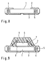
- Figures 9, 10(a), and 10(b) show a conventional semiconductor package for a card-type memory device.
- Figure 9 is a cross-sectional view of the semiconductor package
- Figure 10(a) is a perspective view of the chip side of the semiconductor package
- Figure 10(b) is a perspective view of the external terminal side of the semiconductor package.
- a substrate 1 is formed of resin, which has a thickness of approximately 0.1 - 0.4 mm, and a semiconductor chip 6 is bonded to the substrate 1 by an adhesive 9.
- a gold wire 7 provides an electrical connection between a chip connection terminal 2 of the substrate 1 and a bonding pad of tile semiconductor chip 6.
- the chip side of the substrate 1 is molded by a resin 8 that covers the semiconductor chip 6, and an external connection terminal 3 is provided on the other side of the substrate 1.
- the external connection terminal 3 is electrically connected to the chip connection terminal 2 via a through-hole 4 that penetrates the substrate 1.
- FIG 8 shows a cross-sectional view of the substrate used in the conventional semiconductor package of Figure 9.
- the chip connection terminal 2 which is located on the chip side of the substrate 1, is typically plated with soft gold with a purity of 99.9% or higher.
- the soft gold on the chip connection terminal 2 provides a good connection between the bonding wire 7 and the chip connection terminal 2 because soft gold or aluminum is typically used for the bonding wire that is connected between the chip's bonding pad and the chip connection terminal of the substrate 1.
- the external connection terminal 3 which is located on the side of the substrate opposite the semiconductor chip 6, is typically plated with hard gold with a purity of approximately 99%.
- Hard gold is used for the external connection terminal because it offers a greater resistance to damage.
- a boundary 5 between the soft gold plating and the hard gold plating is located at a central portion of the through-hole 4.
- Figure 8 does not individually show the gold plating, nickel plating, and copper plating and foil that are described below. These layers are collectively shown as the chip connection terminal and the external connection terminal in Figure 8.
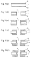
- FIGs 11(a) through 11(f) show a typical manufacturing process for the conventional semiconductor device substrate described above.
- copper foils 24 with an illustrative thickness of about 18 ⁇ m are attached using an adhesive to both sides of a resin substrate 1, as shown in Figure 11(a).
- the substrate 1 is then drilled to open a through-hole 4, as shown in Figure 11(b).
- the entire substrate is plated with copper so that copper plating 25 is provided on the inner side of the through-hole and on both sides of the substrate.
- the copper plating provides an electrical connection between the two sides of the substrate.
- a photoresist-type dry film is then pasted onto the copper of the substrate and a copper interconnection is formed through exposure of light, patterning, and etching of the copper, as shown in Figure 11(d).
- the copper interconnections are typically formed of both copper foils and copper plating because the copper foils can be used to easily and quickly increase the thickness of the connection by merely pasting them onto the substrate.
- the copper foil cannot be attached to the inner side of the through-hole to complete the interconnection.
- it is rather difficult to increase the thickness of the connection terminal through copper plating because of the slow progress of the plating process. In cases where a low relative thickness or slow progress are not drawbacks, it is possible to omit the copper foils and use only the copper plating to form the copper interconnections.
- the chip-mounting side of the substrate is entirely masked using a tape or photoresist-type dry film.
- Bright nickel (not shown) and hard gold are then consecutively plated on the substrate to provide a hard gold plating 3 over the copper interconnection on the external terminal side of the substrate and on the inside of the through-hole 4, as shown in Figure 11(e).
- the hard gold-plated external terminal side of the substrate is entirely masked using a tape or dry film.
- Non-bright or semi-bright nickel (not shown) and soft gold are then consecutively plated on the substrate to provide soft gold plating 2 over the copper interconnection on the chip-mounting side of the substrate and on the inside of the through-hole 4, as shown in Figure 11(f).
- the nickel plating is interposed between the copper plating and the gold plating because the intervening nickel layer prevents a slow diffusion of the gold into the copper.
- the order of the gold plating is reversed so that soft gold is first plated on the chip-mounting side and then hard gold is plated on the external terminal side of the substrate.
- one side of the through-hole 4 is closed by the masking during both soil gold and hard gold plating.
- air builds up in the through-hole 4 and the plating solution is prevented from flowing through the through-hole 4. Therefore, ⁇ in some cases, no plating is attained at the central portion of the through-hole 4.
- the through-hole 4 has portions that are not plated by either the soil gold or hard gold, the underlying metal layer of copper or nickel is exposed to oxygen and the like. This allows corrosive action to occur in the exposed portion of the through-hole so that a breakage of the interconnection between the two sides of the substrate may result.
- the present invention to remove the above-mentioned drawbacks and to provide a semiconductor substrate in which the inside of the through-hole is completely plated in order to improve the reliability of the interconnection.
- the through-hole in the substrate is not blocked when it is selectively plated.
- the plating solution readily flows through and near the through-hole so that plating is provided on the surface of the through-hole. Thug, there is no plating boundary located within the through-hole, so corrosive action is prevented in the underlying layers in the through-hole portion and the reliability of the interconnection that passes through the through-hole is improved.
- the present invention also provides a method of manufacturing such a device.
- a semiconductor device that includes a substrate having a first side, a second side, and a through-hole.
- An external connection terminal is located on the first side of the substrate, and a chip connection terminal is located on the second side of the substrate.
- the chip connection terminal is electrically connected to the external connection terminal via the through-hole.
- the external connection terminal, the inner portion of the through hole, and a first portion of the chip connection terminal have a hard gold plating, and a second portion of the chip connection terminal has a soft gold plating.
- a semiconductor device that includes a substrate having a first side, a second side, and a through-hole.
- An external connection terminal is located on the first side of the substrate, and a chip connection terminal is located on the second side of the substrate.
- the chip connection terminal is electrically connected to the external connection terminal via the through-hole.
- the chip connection terminal, the inner portion of the through hole, and a first portion of the external connection terminal have a soft plating, and a second portion of the external connection terminal has a hard gold plating.
- a method for manufacturing a semiconductor device by making an interconnection pattern of copper plating on a first side and a second side of a substrate and on the inner side of a through-hole.
- a first mask is formed on the first side of the substrate so as to cover a portion of the interconnection pattern on the first side without covering the through-hole.
- Nickel and then hard gold are plated on the portion of the interconnection pattern that is not covered by the first mask (including the inner side of the through-hole), and then the first mask is removed.
- a second mask is then formed to cover the portion of the interconnection pattern that was plated with hard gold. Nickel and then soft gold are plated on the portion of the interconnection pattern that is not covered by the second mask, and then the second mask is removed.
- a method for manufacturing a semiconductor device by making an interconnection pattern of copper plating on a first side and a second side of a substrate and on the inner side of a through-hole.
- a first mask is formed on the first side of the substrate so as to cover a portion of the interconnection pattern on the first side and the through-hole.
- Nickel and then soft gold are plated on the portion of the interconnection pattern that is not covered by the first mask, and then the first mask is removed.
- a second mask is then formed to cover the portion of the interconnection pattern that was plated with soft gold. Nickel and then hard gold are plated on the portion of the interconnection pattern that is not covered by the second mask (including the inner side of the through-hole), and then the second mask is removed.
- a semiconductor device includes a substrate having a first side, a second side, and a through-hole.
- An external connection terminal is located on the first side of the substrate, and a chip connection terminal is located on the second side of the substrate.
- the chip connection terminal is electrically connected to the external connection terminal via the through-hole.
- a semiconductor chip is attached to the second side of the substrate and electrically connected to the chip connection terminal, and a resin molding covers at least a portion of the second side of the substrate.
- the external connection terminal, the inner portion of the through hole, and a first portion of the chip connection terminal have a hard gold plating, and a second portion of the chip connection terminal has a soft gold plating.
- a semiconductor device includes a substrate having a first side, a second side, and a through-hole.
- An external connection terminal is located on the first side of the substrate, and a chip connection terminal is located on the second side of the substrate.
- the chip connection terminal is electrically connected to the external connection terminal via the through-hole.
- a semiconductor chip is attached to the second side of the substrate and electrically connected to the chip connection terminal, and a resin molding covers at least a portion of the second side of the substrate.
- the chip connection terminal, the inner portion of the through hole, and a first portion of the external connection terminal have a soft plating, and a second portion of the external connection terminal has a hard gold plating.
- the some embodiments of the present invention provide a card-type module that includes the semiconductor device of the previously-described embodiments. Additionally, some embodiments of the present invention provide a memory device having such a card-type module and a main body.
- the main body includes a first connector connected to the external connection terminal of the card-type module, a second connector connected to an apparatus, and an interface control circuit connected to the first and second connectors.
- Figure 1 shows a semiconductor device substrate according to a preferred embodiment of the present invention
- Figure 6 shows a preferred manufacturing process for the semiconductor device substrate of Figure 1.
- copper foils 24 with an illustrative thickness of 18 ⁇ m are attached using an adhesive to both sides of a resin substrate 1, as shown in Figure 6(a).
- the substrate is a high strength substrate formed of a glass fiber framework that is covered by an epoxy resin.
- a through-hole 4 is then formed by drilling through the substrate, as shown in Figure 6(b).
- Figure 6(c) the entire substrate is plated with copper so that copper plating 25 is provided on the inner side of the through-hole 4 and on both sides of the substrate 1.
- the copper plating 25, which provides an electrical connection between the two sides of the substrate, is illustratively formed with a thickness of about 10 to 15 ⁇ m.
- a copper interconnection is then formed using a photoresist-type dry film or the like. For example, when a dry film is used, it is pasted onto the copper 25 of the substrate and a copper interconnection is formed by sequentially performing exposure to light, patterning, and etching of the copper.
- the portion of the interconnection on the chip-mounting side of the substrate is masked.
- the through-hole 4 is not masked.
- Such a mask can be formed by adhering a pre-shaped tape to the substrate, or by applying a dry film over the entire chip-mounting side of the substrate and then patterning the film using a lithography technique or the like.
- the substrate is then consecutively subjected to bright-nickel plating (not shown) and hard gold plating to provide a hard gold plating 3 over the interconnection pattern, as shown in Figure 6(e). Because the through-hole 4 is not closed at its top or bottom by the mask, the plating solution readily flows through and near the through-hole 4.
- the hard gold plating 3 covers the entire copper interconnection on the external terminal side of the substrate, the entire copper interconnection layer on the inner side of the through-hole 4, and the unmasked portion of the copper interconnection on the chip-mounting side of the substrate.
- the hard gold-plated portion 3 is newly masked in the same manner as described above. Then, the unmasked portion is consecutively subjected to non-bright nickel plating (not shown) and soft gold plating to provide a soft gold plating 2 over the interconnection pattern. The new mask is then also removed. As a result, the soft-gold plating 2 is provided on the unmasked portion of the chip connection terminal (of the copper interconnection) on the chip-mounting side of the substrate, as shown in Figure 6(f).
- Figures 1-3 do not individually show the gold plating, nickel plating, and copper plating and foil described above. These layers are collectively shown as the chip connection terminal and the external connection terminal in these figures.
- the entire copper interconnection layer on the inner side of the through-hole 4 is covered with the hard gold plating 3 so that the boundary 5 between the soft gold plating and the hard gold plating is located outside of the through-hole 4.
- the above gold plating order is reversed. That is, soft gold is first plated to the chip connection terminal on the chip-mounting side of the substrate, and then hard gold is plated on the entire copper interconnection on the external terminal side of the substrate, the entire copper interconnection layer on the inner side of the through-hole 4, and the non-soft gold plated portion of the copper interconnection on the chip-mounting side of the substrate.
- FIG 4 shows a top view of the semiconductor device substrate of Figure 1.
- An interconnection 12 extends from a chip connection terminal 11, through a through-hole 4, and to an external connection terminal on the opposite side of the substrate 1.
- a semiconductor chip is mounted on a chip mount surface portion 13 of the substrate, and resin molding is performed on the area within resin molding boundary line 14.
- a cutting line 15 shows the line along which the semiconductor module is cut after the substrate 1 is mounted with a semiconductor chip and then resin molded.
- a gold plating boundary line 16 represents a boundary between the soft gold plating and the hard gold plating of the interconnections. More specifically, the inner side of the gold plating boundary line 16 is plated with soft gold, and the outer side is plated with hard gold. In further embodiments, the gold plating boundary line 16 is on the outer side of the resin molding boundary line 14.
- FIG. 2 shows a semiconductor package according to a preferred embodiment of the present invention.
- the semiconductor package is formed by bonding a semiconductor chip 6 to the substrate of Figure 1 by an adhesive 9.
- a bonding pad of the semiconductor chip 6 is connected by a gold wire 7 to the chip connection terminal of the substrate 1, and the chip-mounting side of the substrate is molded by resin 8.
- the resin 8 is an epoxy resin and the semiconductor chip is a nonvolatile semiconductor memory device such as a NAND-type Flash EEPROM.
- the chip may be any type of semiconductor chip.
- the semiconductor chip is connected to the chip connection terminal of the substrate through a flip-chip-type connection that utilizes a bump 10, as shown in Figure 3.
- the semiconductor packages of Figures 2 and 3 may be used in a card-type module, as shown in Figure 5.
- the card-type module is smaller than a typical IC card, which is connected to a personal computer or the like.
- the card-type module employs a base card 18 that is illustratively formed of resin and has an illustrative length, width, and thickness of 37 mm by 45 mm by 0.76 mm.
- the base card is provided with a recessed portion 18a that holds the semiconductor package.
- the semiconductor package 17 is bonded to the base card 18 by burying the resin-molded side of the semiconductor package 17 into the recessed portion 18a of the base card in such a manner that the external terminal 3 side of the package is flush with the surface of the base card 18.
- the card-type module contains a nonvolatile semiconductor memory device so that it is analogous to a floppy disk. That is, the card-type module contains the storage portion but not the driver portion of the complete storage device.
- the driver portion i.e., processing circuitry and the like
- the storage portion of the memory device can be exchanged, just like a floppy disk, by exchanging the card-type module.
- Figures 7(a) and 7(b) show an adapter card that allows the card-type module of Figure 5 to be connected to a PCMCIA card slot or the like so that the card-type module can be interfaced with a personal computer, digital camera, or other electronic device.
- the adapter card 20 has the outer appearance of a PCMCIA card and includes an insertion hole 20a for receiving a card-type module 19.
- one connector 23 allows the adaptor card to be attached to the PCMCIA card slot of a personal computer, electronic device, or the like, and another connector 22 in the interior of the adapter card 20 contacts with the external connection terminals 3 of the card-type module 19.
- an interface circuit 21 functions as an interface between the card-type module 19 and an external apparatus, such as a personal computer.
- the adapter is of a form other than the card-type that is attached to a PCMCIA card slot.
- a drive circuit or the like may be provided in the interior of the adapter card 20 to control the card-type module.
- the connector 22 that contacts with the external connection terminals 3 of the card-type module may be provided, typically along with the interface circuit 21 and the like, in the main body of a personal computer, digital camera, or other electronic device.
- the substrate is formed of resin
- the substrate is formed of TAB tape. More specifically, tape automating bonding ("TAB") is used to form a thinner semiconductor package in which the wires connected to the chip electrodes are formed by copper plating on the insulation tape film.
- TAB tape automating bonding
- the semiconductor substrate has hard gold plating located on the external terminal side of the substrate, the inner side of the through-hole, and a portion of the chip-mounting side of the substrate.
- the present invention is not limited to only that specific structure. For example, the sides could be reversed, the soft gold and hard gold plating portions could be switched, or all soft gold plating could be used.
- the present invention provides a semiconductor substrate having a through-hole which is not blocked when it is selectively plated.
- the plating solution readily flows through and near the through-hole so that plating is provided on the surface of the through-hole.
- there is no plating boundary located within the through-hole so corrosive action is prevented in the underlying layers in the through-hole portion.
- the reliability of the interconnection that passes through the through-hole is improved.
Landscapes
- Engineering & Computer Science (AREA)
- Manufacturing & Machinery (AREA)
- Microelectronics & Electronic Packaging (AREA)
- Printing Elements For Providing Electric Connections Between Printed Circuits (AREA)
- Internal Circuitry In Semiconductor Integrated Circuit Devices (AREA)
- Structures Or Materials For Encapsulating Or Coating Semiconductor Devices Or Solid State Devices (AREA)
Applications Claiming Priority (3)
| Application Number | Priority Date | Filing Date | Title |
|---|---|---|---|
| JP138344/96 | 1996-05-31 | ||
| JP13834496 | 1996-05-31 | ||
| JP13834496 | 1996-05-31 |
Publications (3)
| Publication Number | Publication Date |
|---|---|
| EP0810656A2 true EP0810656A2 (de) | 1997-12-03 |
| EP0810656A3 EP0810656A3 (de) | 1998-08-26 |
| EP0810656B1 EP0810656B1 (de) | 2004-10-06 |
Family
ID=15219733
Family Applications (1)
| Application Number | Title | Priority Date | Filing Date |
|---|---|---|---|
| EP97108766A Expired - Lifetime EP0810656B1 (de) | 1996-05-31 | 1997-06-02 | Halbleitersubstrat und seine Herstellung |
Country Status (6)
| Country | Link |
|---|---|
| US (1) | US6091137A (de) |
| EP (1) | EP0810656B1 (de) |
| KR (1) | KR100280170B1 (de) |
| CN (1) | CN1146040C (de) |
| DE (1) | DE69731028T2 (de) |
| TW (1) | TW332334B (de) |
Cited By (2)
| Publication number | Priority date | Publication date | Assignee | Title |
|---|---|---|---|---|
| US6798058B1 (en) | 1999-02-18 | 2004-09-28 | Seiko Epson Corporation | Semiconductor device, mounting and method of manufacturing mounting substrate, circuit board, and electronic instrument |
| CN103237416A (zh) * | 2013-05-08 | 2013-08-07 | 无锡江南计算技术研究所 | 同一表面实现电镀硬金和电镀软金的图形制作方法 |
Families Citing this family (28)
| Publication number | Priority date | Publication date | Assignee | Title |
|---|---|---|---|---|
| US5952716A (en) * | 1997-04-16 | 1999-09-14 | International Business Machines Corporation | Pin attach structure for an electronic package |
| SE512710C2 (sv) * | 1998-07-08 | 2000-05-02 | Ericsson Telefon Ab L M | Kapsel för högeffekttransistorchip för höga frekvenser innefattande en elektriskt och termiskt ledande fläns |
| US6599147B1 (en) * | 1999-05-11 | 2003-07-29 | Socket Communications, Inc. | High-density removable expansion module having I/O and second-level-removable expansion memory |
| US6353870B1 (en) * | 1999-05-11 | 2002-03-05 | Socket Communications Inc. | Closed case removable expansion card having interconnect and adapter circuitry for both I/O and removable memory |
| US6600214B2 (en) * | 2000-05-15 | 2003-07-29 | Hitachi Aic Inc. | Electronic component device and method of manufacturing the same |
| JP2002092575A (ja) * | 2000-09-19 | 2002-03-29 | Mitsubishi Electric Corp | 小型カードとその製造方法 |
| US6774486B2 (en) | 2001-10-10 | 2004-08-10 | Micron Technology, Inc. | Circuit boards containing vias and methods for producing same |
| WO2003088021A2 (en) * | 2002-04-08 | 2003-10-23 | Socket Communications, Inc | Wireless enabled memory module |
| TWI234210B (en) * | 2002-12-03 | 2005-06-11 | Sanyo Electric Co | Semiconductor module and manufacturing method thereof as well as wiring member of thin sheet |
| KR100499003B1 (ko) * | 2002-12-12 | 2005-07-01 | 삼성전기주식회사 | 도금 인입선을 사용하지 않는 패키지 기판 및 그 제조 방법 |
| TWI228804B (en) * | 2003-07-02 | 2005-03-01 | Lite On Semiconductor Corp | Chip package substrate having flexible printed circuit board and method for fabricating the same |
| US7240144B2 (en) * | 2004-04-02 | 2007-07-03 | Arm Limited | Arbitration of data transfer requests |
| JP4361826B2 (ja) * | 2004-04-20 | 2009-11-11 | 新光電気工業株式会社 | 半導体装置 |
| KR100723493B1 (ko) * | 2005-07-18 | 2007-06-04 | 삼성전자주식회사 | 와이어 본딩 및 플립 칩 본딩이 가능한 스마트 카드 모듈기판 및 이를 포함하는 스마트 카드 모듈 |
| US20080237842A1 (en) * | 2007-03-29 | 2008-10-02 | Manepalli Rahul N | Thermally conductive molding compounds for heat dissipation in semiconductor packages |
| JP2009206429A (ja) | 2008-02-29 | 2009-09-10 | Toshiba Corp | 記憶媒体 |
| US8084348B2 (en) * | 2008-06-04 | 2011-12-27 | Oracle America, Inc. | Contact pads for silicon chip packages |
| KR20100033012A (ko) | 2008-09-19 | 2010-03-29 | 주식회사 하이닉스반도체 | 반도체 패키지 및 이를 갖는 적층 반도체 패키지 |
| USD794644S1 (en) * | 2009-01-07 | 2017-08-15 | Samsung Electronics Co., Ltd. | Memory device |
| USD794034S1 (en) * | 2009-01-07 | 2017-08-08 | Samsung Electronics Co., Ltd. | Memory device |
| USD794642S1 (en) * | 2009-01-07 | 2017-08-15 | Samsung Electronics Co., Ltd. | Memory device |
| USD795261S1 (en) * | 2009-01-07 | 2017-08-22 | Samsung Electronics Co., Ltd. | Memory device |
| USD794643S1 (en) * | 2009-01-07 | 2017-08-15 | Samsung Electronics Co., Ltd. | Memory device |
| USD794641S1 (en) * | 2009-01-07 | 2017-08-15 | Samsung Electronics Co., Ltd. | Memory device |
| USD795262S1 (en) * | 2009-01-07 | 2017-08-22 | Samsung Electronics Co., Ltd. | Memory device |
| US8407888B2 (en) | 2010-05-07 | 2013-04-02 | Oracle International Corporation | Method of assembling a circuit board assembly |
| CN102339404B (zh) * | 2010-07-20 | 2016-06-15 | 上海仪电智能电子有限公司 | 一种新型智能卡模块及其生产工艺 |
| TWI408837B (zh) * | 2011-02-08 | 2013-09-11 | 旭德科技股份有限公司 | 封裝載板及其製作方法 |
Family Cites Families (45)
| Publication number | Priority date | Publication date | Assignee | Title |
|---|---|---|---|---|
| US3663376A (en) * | 1971-03-17 | 1972-05-16 | Gary Uchytil | Selective spot plating of lead frame sheets |
| FR2439478A1 (fr) * | 1978-10-19 | 1980-05-16 | Cii Honeywell Bull | Boitier plat pour dispositifs a circuits integres |
| JPS5990938A (ja) * | 1982-11-17 | 1984-05-25 | Nec Corp | 半導体装置用プリント回路基板 |
| US4703420A (en) * | 1985-02-28 | 1987-10-27 | International Business Machines Corporation | System for arbitrating use of I/O bus by co-processor and higher priority I/O units in which co-processor automatically request bus access in anticipation of need |
| DE3531318A1 (de) * | 1985-09-02 | 1987-03-05 | Allied Corp | Kontaktiereinrichtung fuer eine chip-karte |
| US4882702A (en) * | 1986-03-31 | 1989-11-21 | Allen-Bradley Company, Inc. | Programmable controller with I/O expansion module located in one of I/O module positions for communication with outside I/O modules |
| US4837628A (en) * | 1986-07-14 | 1989-06-06 | Kabushiki Kaisha Toshiba | Electronic still camera for recording still picture on memory card with mode selecting shutter release |
| US4980856A (en) * | 1986-10-20 | 1990-12-25 | Brother Kogyo Kabushiki Kaisha | IC memory cartridge and a method for providing external IC memory cartridges to an electronic device extending end-to-end |
| JPS6478397A (en) * | 1987-09-18 | 1989-03-23 | Mitsubishi Electric Corp | Ic card writing system |
| FR2624635B1 (fr) * | 1987-12-14 | 1991-05-10 | Sgs Thomson Microelectronics | Support de composant electronique pour carte memoire et produit ainsi obtenu |
| US5018017A (en) * | 1987-12-25 | 1991-05-21 | Kabushiki Kaisha Toshiba | Electronic still camera and image recording method thereof |
| JPH0795577B2 (ja) * | 1988-04-12 | 1995-10-11 | 富士プラント工業株式会社 | リードフレームへの部分メッキ方法 |
| JP2565387B2 (ja) * | 1988-10-28 | 1996-12-18 | イビデン株式会社 | Icカード用プリント配線板とその製造方法 |
| US5184282A (en) * | 1989-02-27 | 1993-02-02 | Mips Co., Ltd. | IC card adapter |
| JPH02111861U (de) * | 1989-02-27 | 1990-09-06 | ||
| US5535328A (en) * | 1989-04-13 | 1996-07-09 | Sandisk Corporation | Non-volatile memory system card with flash erasable sectors of EEprom cells including a mechanism for substituting defective cells |
| US5172338B1 (en) * | 1989-04-13 | 1997-07-08 | Sandisk Corp | Multi-state eeprom read and write circuits and techniques |
| DE69034227T2 (de) * | 1989-04-13 | 2007-05-03 | Sandisk Corp., Sunnyvale | EEprom-System mit Blocklöschung |
| US5457590A (en) * | 1989-12-12 | 1995-10-10 | Smartdiskette Gmbh | Insertable element for a disk station of EDP equipment with connections to external components |
| US5153818A (en) * | 1990-04-20 | 1992-10-06 | Rohm Co., Ltd. | Ic memory card with an anisotropic conductive rubber interconnector |
| JPH0416396A (ja) * | 1990-05-10 | 1992-01-21 | Mitsubishi Electric Corp | 半導体装置カード |
| JP2560895B2 (ja) * | 1990-07-25 | 1996-12-04 | 三菱電機株式会社 | Icカードの製造方法およびicカード |
| US5293236A (en) * | 1991-01-11 | 1994-03-08 | Fuji Photo Film Co., Ltd. | Electronic still camera including an EEPROM memory card and having a continuous shoot mode |
| US5663901A (en) * | 1991-04-11 | 1997-09-02 | Sandisk Corporation | Computer memory cards using flash EEPROM integrated circuit chips and memory-controller systems |
| DE4121023C2 (de) * | 1991-06-26 | 1994-06-01 | Smartdiskette Gmbh | In eine EDV-Einrichtung einsteckbares Element |
| US5430859A (en) * | 1991-07-26 | 1995-07-04 | Sundisk Corporation | Solid state memory system including plural memory chips and a serialized bus |
| US5299089A (en) * | 1991-10-28 | 1994-03-29 | E. I. Dupont De Nemours & Co. | Connector device having two storage decks and three contact arrays for one hard disk drive package or two memory cards |
| FR2686172B1 (fr) * | 1992-01-14 | 1996-09-06 | Gemplus Card Int | Carte enfichable pour microordinateur formant lecteur de carte a contacts affleurants. |
| JPH06105271A (ja) * | 1992-09-16 | 1994-04-15 | Asahi Optical Co Ltd | Icメモリカードカメラシステム |
| US5343319A (en) * | 1993-06-14 | 1994-08-30 | Motorola, Inc. | Apparatus for adapting an electrical communications port to an optical communications port |
| EP0620933A4 (de) * | 1992-11-12 | 1995-03-01 | New Media Corp | Rekonfigurierbare schnittstelle zwischen einem rechner und peripheriegeraeten. |
| US5475441A (en) * | 1992-12-10 | 1995-12-12 | Eastman Kodak Company | Electronic camera with memory card interface to a computer |
| US5469399A (en) * | 1993-03-16 | 1995-11-21 | Kabushiki Kaisha Toshiba | Semiconductor memory, memory card, and method of driving power supply for EEPROM |
| US5488433A (en) * | 1993-04-21 | 1996-01-30 | Kinya Washino | Dual compression format digital video production system |
| JPH0737049A (ja) * | 1993-07-23 | 1995-02-07 | Toshiba Corp | 外部記憶装置 |
| US5887145A (en) * | 1993-09-01 | 1999-03-23 | Sandisk Corporation | Removable mother/daughter peripheral card |
| JPH07321155A (ja) * | 1994-05-25 | 1995-12-08 | Hitachi Cable Ltd | Tabテープキャリアの製造方法 |
| KR0144818B1 (ko) * | 1994-07-25 | 1998-08-17 | 김광호 | 낸드형 플래쉬메모리 아이씨카드 |
| FR2723257B1 (fr) * | 1994-07-26 | 1997-01-24 | Sgs Thomson Microelectronics | Boitier bga de circuit integre |
| US5611057A (en) * | 1994-10-06 | 1997-03-11 | Dell Usa, L.P. | Computer system modular add-in daughter card for an adapter card which also functions as an independent add-in card |
| US5508971A (en) * | 1994-10-17 | 1996-04-16 | Sandisk Corporation | Programmable power generation circuit for flash EEPROM memory systems |
| JPH08139456A (ja) * | 1994-11-10 | 1996-05-31 | Hitachi Chem Co Ltd | 半導体搭載用多層配線板の製造法 |
| KR0152042B1 (ko) * | 1995-04-15 | 1998-10-15 | 김광호 | 낸드형 플래쉬메모리 아이씨카드 기록장치 |
| JPH08319456A (ja) * | 1995-04-28 | 1996-12-03 | E I Du Pont De Nemours & Co | 印刷回路用の水系処理可能な軟質の光画像化可能耐久被覆材 |
| US5596532A (en) * | 1995-10-18 | 1997-01-21 | Sandisk Corporation | Flash EEPROM self-adaptive voltage generation circuit operative within a continuous voltage source range |
-
1997
- 1997-05-28 TW TW086107247A patent/TW332334B/zh not_active IP Right Cessation
- 1997-05-29 US US08/864,958 patent/US6091137A/en not_active Expired - Lifetime
- 1997-05-30 CN CNB971149046A patent/CN1146040C/zh not_active Expired - Fee Related
- 1997-05-30 KR KR1019970021875A patent/KR100280170B1/ko not_active Expired - Fee Related
- 1997-06-02 EP EP97108766A patent/EP0810656B1/de not_active Expired - Lifetime
- 1997-06-02 DE DE69731028T patent/DE69731028T2/de not_active Expired - Lifetime
Cited By (5)
| Publication number | Priority date | Publication date | Assignee | Title |
|---|---|---|---|---|
| US6798058B1 (en) | 1999-02-18 | 2004-09-28 | Seiko Epson Corporation | Semiconductor device, mounting and method of manufacturing mounting substrate, circuit board, and electronic instrument |
| US7163613B2 (en) | 1999-02-18 | 2007-01-16 | Seiko Epson Corporation | Method of manufacturing a semiconductor device by forming plating layers having differing thicknesses |
| US8110245B2 (en) | 1999-02-18 | 2012-02-07 | Seiko Epson Corporation | Semiconductor device, mounting substrate and method of manufacturing mounting substrate, circuit board, and electronic instrument |
| CN103237416A (zh) * | 2013-05-08 | 2013-08-07 | 无锡江南计算技术研究所 | 同一表面实现电镀硬金和电镀软金的图形制作方法 |
| CN103237416B (zh) * | 2013-05-08 | 2015-10-07 | 无锡江南计算技术研究所 | 同一表面实现电镀硬金和电镀软金的图形制作方法 |
Also Published As
| Publication number | Publication date |
|---|---|
| CN1170960A (zh) | 1998-01-21 |
| TW332334B (en) | 1998-05-21 |
| EP0810656A3 (de) | 1998-08-26 |
| CN1146040C (zh) | 2004-04-14 |
| KR100280170B1 (ko) | 2001-02-01 |
| DE69731028T2 (de) | 2005-10-06 |
| KR970077542A (ko) | 1997-12-12 |
| DE69731028D1 (de) | 2004-11-11 |
| EP0810656B1 (de) | 2004-10-06 |
| US6091137A (en) | 2000-07-18 |
Similar Documents
| Publication | Publication Date | Title |
|---|---|---|
| EP0810656B1 (de) | Halbleitersubstrat und seine Herstellung | |
| US7293716B1 (en) | Secure digital memory card using land grid array structure | |
| KR100447313B1 (ko) | 반도체 장치 및 그 제조방법 | |
| TWI402950B (zh) | 具單邊遮蓋的系統封裝模組 | |
| US6569712B2 (en) | Structure of a ball-grid array package substrate and processes for producing thereof | |
| KR940003375B1 (ko) | 반도체 장치 및 그 제조 방법 | |
| US6731010B2 (en) | Resin sealed stacked semiconductor packages with flat surfaces | |
| EP0632682A1 (de) | Elastische Leitung zur Oberflächenmontage einer Chippackung auf einem Substrat | |
| EP0942392A2 (de) | Chipkarte | |
| KR20040051310A (ko) | 도금 인입선을 사용하지 않는 패키지 기판 및 그 제조 방법 | |
| JPWO1998018161A1 (ja) | 半導体装置及びその製造方法、回路基板並びにフィルムキャリアテープ | |
| JPH08316362A (ja) | 半導体装置用基板、半導体装置および半導体装置の製造方法 | |
| EP1171915B1 (de) | Elektrische leiteranordnung für ein halbleiterbauelement und verfahren zu ihrer herstellung | |
| US7633763B1 (en) | Double mold memory card and its manufacturing method | |
| US20040124516A1 (en) | Circuit device, circuit module, and method for manufacturing circuit device | |
| EP0803901B1 (de) | Montageverfahren für eine Mehrzahl von Halbleiteranordnungen in korrespondierenden Trägern | |
| JP3475569B2 (ja) | パッケージ及びその製造方法 | |
| JP3137323B2 (ja) | 半導体装置及びその製造方法 | |
| US20010001507A1 (en) | Substrate for a semiconductor device, a semiconductor device, a card type module, and a data memory device | |
| US7220915B1 (en) | Memory card and its manufacturing method | |
| JP3351711B2 (ja) | 半導体装置用基板及びその製造方法、及び半導体装置、カード型モジュール、情報記憶装置 | |
| JPS61145696A (ja) | Icカ−ド | |
| KR100195510B1 (ko) | 칩 카드 | |
| JP3976984B2 (ja) | 半導体装置及びその製造方法 | |
| KR100386636B1 (ko) | 반도체 패키지용 인쇄회로기판의 제조방법 |
Legal Events
| Date | Code | Title | Description |
|---|---|---|---|
| PUAI | Public reference made under article 153(3) epc to a published international application that has entered the european phase |
Free format text: ORIGINAL CODE: 0009012 |
|
| AK | Designated contracting states |
Kind code of ref document: A2 Designated state(s): DE FR GB |
|
| PUAL | Search report despatched |
Free format text: ORIGINAL CODE: 0009013 |
|
| AK | Designated contracting states |
Kind code of ref document: A3 Designated state(s): AT BE CH DE DK ES FI FR GB GR IE IT LI LU MC NL PT SE |
|
| 17P | Request for examination filed |
Effective date: 19980930 |
|
| AKX | Designation fees paid |
Free format text: DE FR GB |
|
| RBV | Designated contracting states (corrected) |
Designated state(s): DE FR GB |
|
| 17Q | First examination report despatched |
Effective date: 20010117 |
|
| GRAP | Despatch of communication of intention to grant a patent |
Free format text: ORIGINAL CODE: EPIDOSNIGR1 |
|
| GRAS | Grant fee paid |
Free format text: ORIGINAL CODE: EPIDOSNIGR3 |
|
| GRAA | (expected) grant |
Free format text: ORIGINAL CODE: 0009210 |
|
| AK | Designated contracting states |
Kind code of ref document: B1 Designated state(s): DE FR GB |
|
| REG | Reference to a national code |
Ref country code: GB Ref legal event code: FG4D |
|
| REF | Corresponds to: |
Ref document number: 69731028 Country of ref document: DE Date of ref document: 20041111 Kind code of ref document: P |
|
| ET | Fr: translation filed | ||
| PLBE | No opposition filed within time limit |
Free format text: ORIGINAL CODE: 0009261 |
|
| STAA | Information on the status of an ep patent application or granted ep patent |
Free format text: STATUS: NO OPPOSITION FILED WITHIN TIME LIMIT |
|
| 26N | No opposition filed |
Effective date: 20050707 |
|
| PGFP | Annual fee paid to national office [announced via postgrant information from national office to epo] |
Ref country code: FR Payment date: 20110621 Year of fee payment: 15 |
|
| PGFP | Annual fee paid to national office [announced via postgrant information from national office to epo] |
Ref country code: GB Payment date: 20110601 Year of fee payment: 15 |
|
| PGFP | Annual fee paid to national office [announced via postgrant information from national office to epo] |
Ref country code: DE Payment date: 20110525 Year of fee payment: 15 |
|
| GBPC | Gb: european patent ceased through non-payment of renewal fee |
Effective date: 20120602 |
|
| REG | Reference to a national code |
Ref country code: FR Ref legal event code: ST Effective date: 20130228 |
|
| REG | Reference to a national code |
Ref country code: DE Ref legal event code: R119 Ref document number: 69731028 Country of ref document: DE Effective date: 20130101 |
|
| PG25 | Lapsed in a contracting state [announced via postgrant information from national office to epo] |
Ref country code: FR Free format text: LAPSE BECAUSE OF NON-PAYMENT OF DUE FEES Effective date: 20120702 Ref country code: DE Free format text: LAPSE BECAUSE OF NON-PAYMENT OF DUE FEES Effective date: 20130101 Ref country code: GB Free format text: LAPSE BECAUSE OF NON-PAYMENT OF DUE FEES Effective date: 20120602 |