EP0809199B1 - Taktverschiebungsunempfindliche Wiederordnung einer Abtastkette - Google Patents
Taktverschiebungsunempfindliche Wiederordnung einer Abtastkette Download PDFInfo
- Publication number
- EP0809199B1 EP0809199B1 EP97303362A EP97303362A EP0809199B1 EP 0809199 B1 EP0809199 B1 EP 0809199B1 EP 97303362 A EP97303362 A EP 97303362A EP 97303362 A EP97303362 A EP 97303362A EP 0809199 B1 EP0809199 B1 EP 0809199B1
- Authority
- EP
- European Patent Office
- Prior art keywords
- clock
- sequential circuit
- scan chain
- clock signal
- scan
- Prior art date
- Legal status (The legal status is an assumption and is not a legal conclusion. Google has not performed a legal analysis and makes no representation as to the accuracy of the status listed.)
- Expired - Lifetime
Links
Images


Classifications
-
- G—PHYSICS
- G01—MEASURING; TESTING
- G01R—MEASURING ELECTRIC VARIABLES; MEASURING MAGNETIC VARIABLES
- G01R31/00—Arrangements for testing electric properties; Arrangements for locating electric faults; Arrangements for electrical testing characterised by what is being tested not provided for elsewhere
- G01R31/28—Testing of electronic circuits, e.g. by signal tracer
- G01R31/317—Testing of digital circuits
- G01R31/3181—Functional testing
- G01R31/3185—Reconfiguring for testing, e.g. LSSD, partitioning
- G01R31/318533—Reconfiguring for testing, e.g. LSSD, partitioning using scanning techniques, e.g. LSSD, Boundary Scan, JTAG
- G01R31/318552—Clock circuits details
-
- G—PHYSICS
- G01—MEASURING; TESTING
- G01R—MEASURING ELECTRIC VARIABLES; MEASURING MAGNETIC VARIABLES
- G01R31/00—Arrangements for testing electric properties; Arrangements for locating electric faults; Arrangements for electrical testing characterised by what is being tested not provided for elsewhere
- G01R31/28—Testing of electronic circuits, e.g. by signal tracer
- G01R31/317—Testing of digital circuits
- G01R31/31725—Timing aspects, e.g. clock distribution, skew, propagation delay
-
- G—PHYSICS
- G01—MEASURING; TESTING
- G01R—MEASURING ELECTRIC VARIABLES; MEASURING MAGNETIC VARIABLES
- G01R31/00—Arrangements for testing electric properties; Arrangements for locating electric faults; Arrangements for electrical testing characterised by what is being tested not provided for elsewhere
- G01R31/28—Testing of electronic circuits, e.g. by signal tracer
- G01R31/317—Testing of digital circuits
- G01R31/3181—Functional testing
- G01R31/3185—Reconfiguring for testing, e.g. LSSD, partitioning
- G01R31/318533—Reconfiguring for testing, e.g. LSSD, partitioning using scanning techniques, e.g. LSSD, Boundary Scan, JTAG
- G01R31/318594—Timing aspects
-
- G—PHYSICS
- G06—COMPUTING OR CALCULATING; COUNTING
- G06F—ELECTRIC DIGITAL DATA PROCESSING
- G06F1/00—Details not covered by groups G06F3/00 - G06F13/00 and G06F21/00
- G06F1/04—Generating or distributing clock signals or signals derived directly therefrom
- G06F1/10—Distribution of clock signals, e.g. skew
Definitions
- the present invention relates to a method of laying out complex circuit designs and in particular, but not exclusively, to a method of reordering a scan chain based on the results of distributing a clock signal to eliminate any scan chain hold time failures and minimize chip area overhead required for the scan chain.
- Integrated circuits utilize a clock signal to control the timing of combinatorial (gates) and sequential (latches, flip-flops) circuit elements contained therein.
- this clock signal must reach the various elements that are physically distributed throughout the integrated circuit at the same time. If the elements are located at varying distances from the source of the clock signal, the clock signal will arrive at different times to the elements over the interconnecting metal leads. This is one cause of a phenomenon known as clock skew. Clock skew can also be caused by the resistance and the capacitance encountered by the clock signal to the various elements. Techniques to compensate for this cause of clock skew include designing the metal leads to have equivalent length and capacitively loading some of the metal leads to equalize the capacitance throughout the clock tree.
- Another technique for minimizing clock skew uses multiple buffers to drive the resistance and capacitance encountered by the clock signal.
- these buffers add propagation delays, which also cause clock skew.
- testability is a scan path method which enables direct application of test vectors to sequential circuit elements.
- the sequential circuit elements are serially connected together to form a scan path.
- a test vector is applied from an input pin to the first sequential circuit element of the scan path.
- a clock (enable) signal stores the value of the test vector as it propagates through the sequential circuit elements.
- the sequential circuit elements function as a shift register.
- the output from the last sequential circuit element is compared with an expected value.
- the clock signals of adjacent sequential circuit elements should not be active at the same time.
- the scan path is reordered during the layout process to minimize the chip area overhead of adding the scan path to the design.
- Examples of such a reordering are disclosed in US-A-5,307,286 to Rusu et al. entitled “METHOD FOR OPTIMIZING AUTOMATIC PLACE AND ROUTE LAYOUT FOR FULL SCAN CIRCUITS" and US-A-5,212,651 to Yabe entitled “SCAN PATH GENERATION WITH FLIP-FLOP REARRANGEMENT ACCORDING TO GEOMETRY OF LOGIC CIRCUIT.”
- US-A-5,307,286 discloses an integrated circuit having flip-flop circuits arranged in rows with buffers that provide signals to those flip-flops.
- the flip-flops are grouped in rows with similar latches and buffers in a manner that scan enable signal terminals, clock lines and other global signal lines are connected between adjacent flip-flops by abutment. Buffer values are then computed to select the correct buffers to be placed in the rows with the flip-flops.
- the scan path connections are direct from one sequential circuit element to another.
- the elements in the scan path are susceptible to hold time failures due to clock skew because of the length of the direct connections between the scan elements.
- a clock signal provided to the buffers in one flip-flop row may be skewed with respect to a clock signal provided to the buffers of a directly connected flip-flop row.
- the clock signals in this case, for example, are provided from different clock buffers of the clock tree.
- US-A-5,212,651 discloses a method of scan path generation. The method places flip-flops in a two-dimensional plane according to original scan path data that represents a sequence according to how the flip-flops would originally be connected in the scan path. The flip-flops are then connected in a sequence that meets geometrical design requirements of a logic circuit.
- Balanced clock tree is a common method for providing low skew clock distribution.
- hold time failures will occur in the scan path.
- a hold time failure occurs when the clock skew between two scan elements is greater than the propagation delay minus the hold time of the scan elements. This is becoming a significant issue in integrated circuit testing because the device propagation delays are reducing and RC induced clock skews are increasing with sub-micron technologies. Thus, there arises a significant problem relating to the ability to use a scan path in an integrated circuit design.
- US-A-5,459,736 discloses a scan path circuit which utilizes at least two test clock signals and additional logic to avoid a malfunction during the scan test due to clock skew.
- An evident disadvantage to the apparatus disclosed in US-A-5,459,736 is that the additional logic and plural clock signals increase the complexity in implementing scan testing.
- the additional logic and wiring of the two test clock signals will increase the amount of chip area required on an integrated circuit.
- the complexity of the timing control of the additional logic and the plural signals will also increase.
- the manufacturing of the integrated circuit will become more complex since the additional logic and plural test clock signals' wiring can require more complex masks and additional steps in fabrication.
- US-A-5,337,321 discloses a series of scan path flip-flops that are clocked by a contra-data-direction clock signal.
- a scan test clock signal is provided to a selector associated with the last flip-flop in the scan path.
- the selector outputs a delayed scan test clock signal which is provided to the last flip-flop and to another selector associated with a preceding flip-flop of the scan path.
- the other selector outputs a further delayed scan test clock signal which is provided to the preceding flip-flop and to yet another selector associated with a next-preceding flip-flop of the scan path. This increasing delay of the scan test clock signal is done for each flip-flop remaining in the scan path.
- the present invention therefore seeks to provide for a method and related device having advantages over known methods and apparatus.
- the present invention can therefore include a method of eliminating scan hold time failures of a scan chain.
- the method uses information resulting from the distribution of a clock signal throughout an integrated circuit.
- a scan chain is reordered according to the results of the distribution of the clock signal.
- the distribution of the clock signal provides separate groups of sequential circuit elements that form the scan chain.
- One method of distributing the clock signal contemplated by the present invention is a clock balancing method.
- connections within and between those groups are made. This eliminates clock signal skew for the scan chain. It also provides for reducing the length of the connections within each group. As a result, there is a corresponding reduction in chip area overhead for integration of the scan chain in the circuit.
- sequential circuit elements are designed so that in the absence of a scan enable signal, for example, they function as a part of the overall design in the integrated circuit.
- the scan enable signal When the scan enable signal is provided, the sequential circuit elements are connected to form a scan chain where the sequential elements are linked together to form one extended shift register.
- These sequential elements are serially clocked to receive generated test vectors.
- a test vector is applied with the scan enable signal, the scan enable signal is then removed, and the integrated circuit is functionally operated for at least one clock pulse.
- the scan enable signal is then provided again and the test vector is scanned out of the extended shift register for comparison with an expected pattern.
- the present invention can include this type of testing.
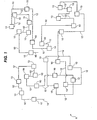
- a scan chain 8 is illustrated that includes sequential circuit elements 10, such as conventional scan chain flip-flops, ordered according to a designer's original scan chain connections 12. Note that the placement of connections 12 is not dictated by the proximity of adjacent sequential circuit elements 10. The connections 12 are not optimized for length, which results in an increased chip area overhead for the scan chain connections 12.
- Connection 14 is typically coupled to an input pad that is coupled to receive the input test vector.
- Connection 16 is typically coupled to an output pad that is coupled to provide the output of scan chain 8.
- clock tree 20 including clock buffers 22 and clock connections 24 are laid out according to a conventional clock balancing technique.
- Figure 2 illustrates such a balanced clock tree that is known in the art. Examples of other methods for clock distribution are mesh and H-tree, which are also known in the art and encompassed by the present invention. Note that sequential circuit elements 10 use the same clock signal.
- the clock balancing process defines the sequential circuit elements 10 into groups 30 having associated clock buffers 22. Sequential circuit elements 10 within each of these groups 30 are close enough to each other so that the clock signal provided by the associated clock buffer 22 will typically have very small skew over clock connections 24. However, if there is skew that will cause hold time problems, the scan chain connecting for the sequential circuit elements 10 can be rearranged to eliminate those problems. Specifically, the scan chain connecting for the sequential circuit elements 10 can be ordered so that each succeeding sequential circuit element 10 in the group receives a clock signal with less skew than the clock signal for the preceding sequential circuit element 10. This reordering method will connect the sequential circuit elements 10 to eliminate all possible hold time failures within the respective groups.
- groups 30 defined by the balancing of the clock tree 20 are used to reorder sequential circuit elements 10. Reordering in this manner will reduce the amount of clock signal skew among the grouped sequential circuit elements 10. The clock signal skew within the groups 30 is less than the clock signal skew for the entire scan chain.
- scan chain connections 12' are optimized, thus reducing chip area overhead for the inclusion of the scan path in an integrated circuit.
- Connection 26 is typically coupled to an input pad that is coupled to receive the input test vector.
- Connection 28 is typically coupled to an output pad that is coupled to provide the output of scan chain 8'.
- Connections between groups 30 can be determined by the relative clock signal skew between groups 30. For example, groups 30 should be ordered so that each succeeding group 30 in the scan chain receives a clock signal with less skew than the clock signal for the preceding group 30. Thus, this reordering method will connect the scan chain of sequential circuit elements 10 to eliminate all possible hold time failures.
- FIG. 4A Another embodiment of the present invention is illustrated in Figures 4A-C.
- a scan chain 118 is illustrated that includes sequential circuit elements 110 that are ordered according to a designer's original scan chain connections 112.
- Connection 114 is typically coupled to an input pad that is coupled to receive the input test vector.
- Connection 116 is typically coupled to an output pad that is coupled to provide the output of scan chain 118.
- Figure 4B shows scan chain 118' reordered according co the physical placement of sequential circuit elements 110 with connections 112'. Although this minimizes the amount of channel space which is occupied by scan chain 118', clock skew has not been taken into account.
- Connection 114' is typically coupled to an input pad that is coupled to receive the input test vector.
- Connection 116' is typically coupled to an output pad that is coupled to provide the output of scan chain 118'.
- each sequential circuit element 110 can be connected to different clock buffers (not shown). This in itself may cause a clock skew among sequential circuit elements 110.
- sequential circuit elements 110 are reordered according to the relative skew among them.
- sequential circuit elements 110 can be ordered so that each succeeding sequential circuit element 110 in the group receives a clock signal with less skew than the clock signal for the preceding sequential circuit element 110. This reordering method will connect the sequential circuit elements 110 to eliminate all possible hold time failures within the respective groups.
- sequential circuit element 110a starts the scan chain because it receives a clock signal (not shown) that has the most skew relative to sequential circuit element 110d.
- Sequential circuit element 110a is connected by connection 112'' to sequential circuit element 110b.
- Sequential circuit element 110b receives a clock signal (not shown) that has less skew than the clock signal provided to sequential circuit element 110a and has greater skew than the clock signal provided to sequential circuit element 110d.
- Sequential circuit element 110b is connected by connection 112'' to sequential circuit element 110c.
- Sequential circuit element 110c receives a clock signal (not shown) that has less skew than the clock signals provided to sequential circuit elements 110a and 110b, and has greater skew than the clock signal provided to sequential circuit element 110d. Reordering sequential elements 110 according to clock skew will eliminate corresponding hold time problems for each respective group of the scan chain.
- Connection 114'' is typically coupled to an input pad that is coupled to receive the input test vector.
- Connection 116'' is typically coupled to an output pad that is coupled to provide the output of scan chain 118''.
Landscapes
- Engineering & Computer Science (AREA)
- Physics & Mathematics (AREA)
- General Engineering & Computer Science (AREA)
- General Physics & Mathematics (AREA)
- Theoretical Computer Science (AREA)
- Tests Of Electronic Circuits (AREA)
- Semiconductor Integrated Circuits (AREA)
- Test And Diagnosis Of Digital Computers (AREA)
Claims (1)
- Verfahren zum Eliminieren von Abtasthaltezeitfehlern an sequentiellen Schaltungselementen, die seriell zu einer Abtastkette (8, 118) geschaltet sind, umfassend die folgenden Schritte:wobei Verbindungen zwischen den Gruppen (3) anhand des relativen Taktversatzes zwischen Gruppen ermittelt werden, so dass die Gruppen (30) so geordnet werden, dass jede nachfolgende Gruppe (30) in der Abtastkette ein Taktsignal mit einem Versatz erhält, der geringer ist als der des Taktsignals für die vorhergehende Gruppe (30), undVerteilen eines Taktsignals, einschließlich des Schrittes des Abgleichens eines Taktbaums (20) aus Taktpuffern (22) und Verbindungen (24) zum Definieren sequentieller Schaltungselemente zu Gruppen (30) mit assoziierten Taktpuffern (22);Ordnen der Abtastkette, die Gruppen von sequentiellen Schaltungselementen (10) beinhaltet;
wobei als Reaktion auf das Vorhandensein eines Haltezeitprobleme verursachendenVersatzes die Abtastkettenverbindung für die sequentiellen Schaltungselemente 10 so umgeordnet wird, dass diese Probleme ausgeschaltet werden; Ordnen der Abtastkette in wenigstens einer Gruppe so, dass jedes nachfolgende sequentielle Schaltungselement 10 in der Gruppe ein Taktsignal mit einem Versatz erhält, der geringer ist als der des Taktsignals für das vorhergehende sequentielle Schaltungselement 10.
Applications Claiming Priority (2)
| Application Number | Priority Date | Filing Date | Title |
|---|---|---|---|
| US08/650,248 US6539509B1 (en) | 1996-05-22 | 1996-05-22 | Clock skew insensitive scan chain reordering |
| US650248 | 1996-05-22 |
Publications (3)
| Publication Number | Publication Date |
|---|---|
| EP0809199A2 EP0809199A2 (de) | 1997-11-26 |
| EP0809199A3 EP0809199A3 (de) | 2000-07-19 |
| EP0809199B1 true EP0809199B1 (de) | 2003-07-30 |
Family
ID=24608110
Family Applications (1)
| Application Number | Title | Priority Date | Filing Date |
|---|---|---|---|
| EP97303362A Expired - Lifetime EP0809199B1 (de) | 1996-05-22 | 1997-05-16 | Taktverschiebungsunempfindliche Wiederordnung einer Abtastkette |
Country Status (5)
| Country | Link |
|---|---|
| US (1) | US6539509B1 (de) |
| EP (1) | EP0809199B1 (de) |
| JP (1) | JPH10104320A (de) |
| KR (1) | KR970076176A (de) |
| DE (1) | DE69723771T2 (de) |
Families Citing this family (14)
| Publication number | Priority date | Publication date | Assignee | Title |
|---|---|---|---|---|
| WO2002071411A1 (en) * | 2001-03-06 | 2002-09-12 | Koninklijke Philips Electronics N.V. | Clock-skew resistant chain of sequential cells |
| US7000163B1 (en) * | 2002-02-25 | 2006-02-14 | Lsi Logic Corporation | Optimized buffering for JTAG boundary scan nets |
| US7392495B1 (en) * | 2002-08-13 | 2008-06-24 | Cypress Semiconductor Corporation | Method and system for providing hybrid clock distribution |
| JP2005032102A (ja) * | 2003-07-09 | 2005-02-03 | Matsushita Electric Ind Co Ltd | スキャンテスト設計方法、スキャンテスト回路、スキャンフリップフロップ回路、スキャンテスト回路挿入用cadプログラム、大規模集積回路及び携帯デジタル機器 |
| US7162673B2 (en) * | 2003-11-14 | 2007-01-09 | Integrated Device Technology, Inc. | Scan chain registers that utilize feedback paths within latch units to support toggling of latch unit outputs during enhanced delay fault testing |
| KR20050078704A (ko) * | 2004-01-31 | 2005-08-08 | 삼성전자주식회사 | 스캔 베이스 atpg 테스트회로, 테스트방법 및 스캔체인 재배열방법 |
| US7421610B2 (en) * | 2005-07-21 | 2008-09-02 | Freescale Semiconductor, Inc. | Clock generation circuit |
| US7987400B2 (en) * | 2008-02-22 | 2011-07-26 | International Business Machines Corporation | Method for optimizing scan chains in an integrated circuit that has multiple levels of hierarchy |
| US8443326B1 (en) | 2012-04-10 | 2013-05-14 | Freescale Semiconductor, Inc. | Scan chain re-ordering in electronic circuit design based on region congestion in layout plan |
| JP5856542B2 (ja) * | 2012-06-11 | 2016-02-09 | 株式会社日立製作所 | 半導体集積回路装置 |
| US8839061B2 (en) | 2013-02-07 | 2014-09-16 | Freescale Semiconductor, Inc. | System and method for scan chain re-ordering |
| GB2540741B (en) * | 2015-07-14 | 2018-05-09 | Advanced Risc Mach Ltd | Clock signal distribution and signal value storage |
| US9627012B1 (en) | 2016-06-29 | 2017-04-18 | International Business Machines Corporation | Shift register with opposite shift data and shift clock directions |
| TWI712947B (zh) | 2019-06-06 | 2020-12-11 | 瑞昱半導體股份有限公司 | 積體電路設計方法與其非暫態電腦可讀取媒體 |
Family Cites Families (21)
| Publication number | Priority date | Publication date | Assignee | Title |
|---|---|---|---|---|
| US4879718A (en) | 1987-11-30 | 1989-11-07 | Tandem Computers Incorporated | Scan data path coupling |
| US5239215A (en) * | 1988-05-16 | 1993-08-24 | Matsushita Electric Industrial Co., Ltd. | Large scale integrated circuit configured to eliminate clock signal skew effects |
| JPH02236779A (ja) | 1989-03-10 | 1990-09-19 | Nec Corp | スキャンパス接続方式 |
| US5305451A (en) * | 1990-09-05 | 1994-04-19 | International Business Machines Corporation | Single phase clock distribution circuit for providing clock signals to multiple chip integrated circuit systems |
| JP2638281B2 (ja) * | 1990-10-08 | 1997-08-06 | 日本電気株式会社 | スキャンパス回路 |
| US5208764A (en) | 1990-10-29 | 1993-05-04 | Sun Microsystems, Inc. | Method for optimizing automatic place and route layout for full scan circuits |
| US5109168A (en) | 1991-02-27 | 1992-04-28 | Sun Microsystems, Inc. | Method and apparatus for the design and optimization of a balanced tree for clock distribution in computer integrated circuits |
| JP2695078B2 (ja) | 1991-06-10 | 1997-12-24 | 株式会社東芝 | データ処理装置クロック信号の分配方法 |
| JPH0582611A (ja) | 1991-09-02 | 1993-04-02 | Rohm Co Ltd | 論理回路のレイアウトパターン検証方法 |
| US5475830A (en) | 1992-01-31 | 1995-12-12 | Quickturn Design Systems, Inc. | Structure and method for providing a reconfigurable emulation circuit without hold time violations |
| JP2871291B2 (ja) * | 1992-05-20 | 1999-03-17 | 日本電気株式会社 | 論理集積回路 |
| JP3013332B2 (ja) * | 1993-08-06 | 2000-02-28 | 松下電器産業株式会社 | スキャンテスト回路の配置配線方法及びその配置配線装置並びに半導体集積回路装置 |
| US5481209A (en) * | 1993-09-20 | 1996-01-02 | Lsi Logic Corporation | Clock distribution and control in an integrated circuit |
| KR950022079A (ko) * | 1993-12-01 | 1995-07-26 | 이헌조 | 클럭 스큐에 의한 불안정현상 방지회로 |
| GB9405804D0 (en) * | 1994-03-24 | 1994-05-11 | Discovision Ass | Scannable latch and method of using the same |
| US5502731A (en) * | 1994-08-18 | 1996-03-26 | International Business Machines Corporation | Delay test coverage without additional dummy latches in a scan-based test design |
| KR0157880B1 (ko) * | 1995-03-29 | 1998-12-15 | 문정환 | 클럭 스큐 제거장치 |
| JPH08320893A (ja) * | 1995-05-24 | 1996-12-03 | Mitsubishi Electric Corp | 論理合成装置、論理合成方法及び半導体集積回路 |
| US5596585A (en) * | 1995-06-07 | 1997-01-21 | Advanced Micro Devices, Inc. | Performance driven BIST technique |
| KR970002691A (ko) * | 1995-06-07 | 1997-01-28 | 고속 시스템에 있어서, 클럭 스큐를 최소화하고 리타임 마진을 극대화 하기 위한 장치 | |
| CA2187466A1 (en) * | 1995-10-19 | 1997-04-20 | Kwang-Ting Cheng | Method for inserting test points for full- and partial-scan built-in self-testing |
-
1996
- 1996-05-22 US US08/650,248 patent/US6539509B1/en not_active Expired - Lifetime
-
1997
- 1997-05-16 EP EP97303362A patent/EP0809199B1/de not_active Expired - Lifetime
- 1997-05-16 DE DE69723771T patent/DE69723771T2/de not_active Expired - Lifetime
- 1997-05-20 JP JP9130108A patent/JPH10104320A/ja active Pending
- 1997-05-22 KR KR1019970020109A patent/KR970076176A/ko not_active Ceased
Also Published As
| Publication number | Publication date |
|---|---|
| EP0809199A2 (de) | 1997-11-26 |
| JPH10104320A (ja) | 1998-04-24 |
| DE69723771D1 (de) | 2003-09-04 |
| US6539509B1 (en) | 2003-03-25 |
| DE69723771T2 (de) | 2004-04-22 |
| EP0809199A3 (de) | 2000-07-19 |
| KR970076176A (ko) | 1997-12-12 |
Similar Documents
| Publication | Publication Date | Title |
|---|---|---|
| EP0809199B1 (de) | Taktverschiebungsunempfindliche Wiederordnung einer Abtastkette | |
| US5717700A (en) | Method for creating a high speed scan-interconnected set of flip-flop elements in an integrated circuit to enable faster scan-based testing | |
| US5719878A (en) | Scannable storage cell and method of operation | |
| US7747973B2 (en) | Clustering circuit paths in electronic circuit design | |
| US7017132B2 (en) | Methodology to optimize hierarchical clock skew by clock delay compensation | |
| JP4160733B2 (ja) | 集積回路内のマクロを横切る配線をマクロ内に設計する方法およびシステム | |
| US6640310B2 (en) | Clock system for multiple component system | |
| EP0289158A2 (de) | Diagnosegerät für ein Datenverarbeitungssystem | |
| JP4748896B2 (ja) | 同期型データ転送処理装置 | |
| Kitahara et al. | A clock-gating method for low-power LSI design | |
| US20030210603A1 (en) | Method and apparatus for performing signal synchronization | |
| US6060924A (en) | Semiconductor integrated circuit which contains scan circuits of different types | |
| US20070016884A1 (en) | Apparatus, method, and medium for designing semiconductor integrated circuit | |
| US6647540B2 (en) | Method for reducing EMI and IR-drop in digital synchronous circuits | |
| US7028273B2 (en) | Delay optimization designing system and delay optimization designing method for a logic circuit and control program | |
| EP0351157B1 (de) | Integrierte Halbleiterschaltungen | |
| EP0544164A1 (de) | Halb auf Kundenwunsch hergestellte integrierte Schaltung mit synchroner Taktschaltung und reduzierter Taktverschiebung | |
| JP3198999B2 (ja) | スキャンパス回路のクロックツリー形成方法 | |
| JPH05233092A (ja) | クロック信号分配方法および分配回路 | |
| US6292411B1 (en) | Delay control circuit synchronous with clock signal | |
| JP3178127B2 (ja) | 自動レイアウト手法による半導体集積回路のブロック配置方法 | |
| US20080155490A1 (en) | Method for Reducing Coupling Noise, Reducing Signal Skew, and Saving Layout Area for an Integrated Circuit | |
| US5649177A (en) | Control logic for very fast clock speeds | |
| JP2993488B2 (ja) | 集積回路の設計方法、集積回路及び記憶媒体 | |
| US20080141207A1 (en) | Wiring Design System of Semiconductor Integrated Circuit, Semiconductor Integrated Circuit, and Wiring Design Program |
Legal Events
| Date | Code | Title | Description |
|---|---|---|---|
| PUAI | Public reference made under article 153(3) epc to a published international application that has entered the european phase |
Free format text: ORIGINAL CODE: 0009012 |
|
| AK | Designated contracting states |
Kind code of ref document: A2 Designated state(s): DE FR GB |
|
| RAP1 | Party data changed (applicant data changed or rights of an application transferred) |
Owner name: SYMBIOS, INC. |
|
| RAP1 | Party data changed (applicant data changed or rights of an application transferred) |
Owner name: LSI LOGIC CORPORATION |
|
| PUAL | Search report despatched |
Free format text: ORIGINAL CODE: 0009013 |
|
| AK | Designated contracting states |
Kind code of ref document: A3 Designated state(s): DE FR GB |
|
| RIC1 | Information provided on ipc code assigned before grant |
Free format text: 7G 06F 17/50 A, 7G 01R 31/3185 B |
|
| 17P | Request for examination filed |
Effective date: 20000915 |
|
| 17Q | First examination report despatched |
Effective date: 20020417 |
|
| GRAH | Despatch of communication of intention to grant a patent |
Free format text: ORIGINAL CODE: EPIDOS IGRA |
|
| GRAH | Despatch of communication of intention to grant a patent |
Free format text: ORIGINAL CODE: EPIDOS IGRA |
|
| GRAA | (expected) grant |
Free format text: ORIGINAL CODE: 0009210 |
|
| AK | Designated contracting states |
Designated state(s): DE FR GB |
|
| REG | Reference to a national code |
Ref country code: GB Ref legal event code: FG4D |
|
| REF | Corresponds to: |
Ref document number: 69723771 Country of ref document: DE Date of ref document: 20030904 Kind code of ref document: P |
|
| ET | Fr: translation filed | ||
| PLBE | No opposition filed within time limit |
Free format text: ORIGINAL CODE: 0009261 |
|
| STAA | Information on the status of an ep patent application or granted ep patent |
Free format text: STATUS: NO OPPOSITION FILED WITHIN TIME LIMIT |
|
| 26N | No opposition filed |
Effective date: 20040504 |
|
| PGFP | Annual fee paid to national office [announced via postgrant information from national office to epo] |
Ref country code: GB Payment date: 20140514 Year of fee payment: 18 |
|
| PGFP | Annual fee paid to national office [announced via postgrant information from national office to epo] |
Ref country code: DE Payment date: 20140515 Year of fee payment: 18 Ref country code: FR Payment date: 20140509 Year of fee payment: 18 |
|
| REG | Reference to a national code |
Ref country code: DE Ref legal event code: R119 Ref document number: 69723771 Country of ref document: DE |
|
| GBPC | Gb: european patent ceased through non-payment of renewal fee |
Effective date: 20150516 |
|
| REG | Reference to a national code |
Ref country code: FR Ref legal event code: ST Effective date: 20160129 |
|
| PG25 | Lapsed in a contracting state [announced via postgrant information from national office to epo] |
Ref country code: GB Free format text: LAPSE BECAUSE OF NON-PAYMENT OF DUE FEES Effective date: 20150516 Ref country code: DE Free format text: LAPSE BECAUSE OF NON-PAYMENT OF DUE FEES Effective date: 20151201 |
|
| PG25 | Lapsed in a contracting state [announced via postgrant information from national office to epo] |
Ref country code: FR Free format text: LAPSE BECAUSE OF NON-PAYMENT OF DUE FEES Effective date: 20150601 |