EP0805557A2 - Vorrichtung mit integrierter Halbleiterschaltung - Google Patents
Vorrichtung mit integrierter Halbleiterschaltung Download PDFInfo
- Publication number
- EP0805557A2 EP0805557A2 EP19970107187 EP97107187A EP0805557A2 EP 0805557 A2 EP0805557 A2 EP 0805557A2 EP 19970107187 EP19970107187 EP 19970107187 EP 97107187 A EP97107187 A EP 97107187A EP 0805557 A2 EP0805557 A2 EP 0805557A2
- Authority
- EP
- European Patent Office
- Prior art keywords
- signal
- circuit
- output
- amplitude
- input
- Prior art date
- Legal status (The legal status is an assumption and is not a legal conclusion. Google has not performed a legal analysis and makes no representation as to the accuracy of the status listed.)
- Withdrawn
Links
Images


Classifications
-
- H—ELECTRICITY
- H10—SEMICONDUCTOR DEVICES; ELECTRIC SOLID-STATE DEVICES NOT OTHERWISE PROVIDED FOR
- H10D—INORGANIC ELECTRIC SEMICONDUCTOR DEVICES
- H10D89/00—Aspects of integrated devices not covered by groups H10D84/00 - H10D88/00
- H10D89/211—Design considerations for internal polarisation
- H10D89/213—Design considerations for internal polarisation in field-effect devices
-
- H—ELECTRICITY
- H03—ELECTRONIC CIRCUITRY
- H03K—PULSE TECHNIQUE
- H03K19/00—Logic circuits, i.e. having at least two inputs acting on one output; Inverting circuits
- H03K19/003—Modifications for increasing the reliability for protection
- H03K19/00369—Modifications for compensating variations of temperature, supply voltage or other physical parameters
- H03K19/00384—Modifications for compensating variations of temperature, supply voltage or other physical parameters in field effect transistor circuits
-
- H—ELECTRICITY
- H03—ELECTRONIC CIRCUITRY
- H03K—PULSE TECHNIQUE
- H03K19/00—Logic circuits, i.e. having at least two inputs acting on one output; Inverting circuits
- H03K19/0175—Coupling arrangements; Interface arrangements
- H03K19/0185—Coupling arrangements; Interface arrangements using field effect transistors only
- H03K19/018507—Interface arrangements
-
- H—ELECTRICITY
- H10—SEMICONDUCTOR DEVICES; ELECTRIC SOLID-STATE DEVICES NOT OTHERWISE PROVIDED FOR
- H10W—GENERIC PACKAGES, INTERCONNECTIONS, CONNECTORS OR OTHER CONSTRUCTIONAL DETAILS OF DEVICES COVERED BY CLASS H10
- H10W72/00—Interconnections or connectors in packages
- H10W72/50—Bond wires
- H10W72/541—Dispositions of bond wires
- H10W72/5445—Dispositions of bond wires being orthogonal to a side surface of the chip, e.g. parallel arrangements
-
- H—ELECTRICITY
- H10—SEMICONDUCTOR DEVICES; ELECTRIC SOLID-STATE DEVICES NOT OTHERWISE PROVIDED FOR
- H10W—GENERIC PACKAGES, INTERCONNECTIONS, CONNECTORS OR OTHER CONSTRUCTIONAL DETAILS OF DEVICES COVERED BY CLASS H10
- H10W72/00—Interconnections or connectors in packages
- H10W72/90—Bond pads, in general
- H10W72/931—Shapes of bond pads
- H10W72/932—Plan-view shape, i.e. in top view
-
- H—ELECTRICITY
- H10—SEMICONDUCTOR DEVICES; ELECTRIC SOLID-STATE DEVICES NOT OTHERWISE PROVIDED FOR
- H10W—GENERIC PACKAGES, INTERCONNECTIONS, CONNECTORS OR OTHER CONSTRUCTIONAL DETAILS OF DEVICES COVERED BY CLASS H10
- H10W90/00—Package configurations
- H10W90/701—Package configurations characterised by the relative positions of pads or connectors relative to package parts
- H10W90/751—Package configurations characterised by the relative positions of pads or connectors relative to package parts of bond wires
- H10W90/753—Package configurations characterised by the relative positions of pads or connectors relative to package parts of bond wires between laterally-adjacent chips
Definitions
- the present invention relates to a semiconductor integrated circuit device having driver circuits each for driving a bus, a clock line or an input/output line of a semiconductor chip.
- one of the methods of reducing the power consumption is to reduce the signal amplitude.
- this method is not easy. The reasons are as follows: first, it is difficult to realize the driver circuit for outputting a small amplitude signal under a low power consumption. Or else, it is difficult to realize a receiver circuit for receiving the small-amplitude signal and returning the received small-amplitude signal to the ordinary amplitude signal under a low power consumption.
- the small-amplitude signals have been so far used for only a part of the circuits whose characteristics are well known (e.g., as with the case of bit line signals of a memory device).
- the signals having an amplitude changing between the supply voltage and the ground voltage have been so far used.
- the power consumption cannot be reduced in the semiconductor integrated circuit device having the driver circuits.
- a first aspect of the present invention provides a semiconductor integrated circuit device, comprising: a bias circuit for generating a predetermined voltage fixed between a first supply voltage and a second supply voltage; a driver circuit for receiving an inversion input signal and a non-inversion input signal each vibrating between the first and second supply voltages, for converting the received input signals into a signal vibrating between an output voltage of said bias circuit and the first supply voltage, and for driving a transfer path by the converted signal; a voltage divider circuit for dividing an output voltage of said bias circuit; and a receiver circuit for detecting the signal for driving the transfer path by use of an output of said voltage divider circuit as a reference voltage, and for converting the detected signal into a signal vibrating between the first supply voltage and the second supply voltage.
- a second aspect of the present invention provides a semiconductor integrated circuit device, comprising: a bias circuit for generating a predetermined voltage fixed between a first supply voltage and a second supply voltage; a driver circuit for receiving an inversion input signal and a non-inversion input signal each vibrating between the first and second supply voltages, for converting the received input signals into a signal vibrating between an output voltage of said bias circuit and the first supply voltage on the basis of an enable signal, and for driving a transfer path by the converted signal or for setting an output thereof to a high impedance; a voltage divider circuit for dividing an output voltage of said bias circuit; and a receiver circuit for detecting the signal for driving the transfer path by use of an output of said voltage divider circuit as a reference voltage, and for converting the detected signal into a signal vibrating between the first supply voltage and the second supply voltage.
- a third aspect of the present invention provides a semiconductor integrated circuit device, comprising: a bias circuit for generating a predetermined voltage fixed between a first supply voltage and a second supply voltage; a driver circuit for receiving an inversion input signal and a non-inversion input signal each vibrating between the first and second supply voltages, for converting the received input signals into two differential signals each vibrating between an output voltage of said bias circuit and the first supply voltage, and for driving two transfer paths by the two differential signals, respectively; and a receiver circuit for detecting the differential signals for driving the transfer paths, and for converting the detected differential signals into a signal vibrating between the first supply voltage and the second supply voltage.
- a fourth aspect of the present invention provides a semiconductor integrated circuit device, comprising: a bias circuit for generating a predetermined voltage fixed between a first supply voltage and a second supply voltage; a driver circuit for receiving an inversion input signal and a non-inversion input signal each vibrating between the first and second supply voltages, for converting the received input signals into two differential signals each vibrating between an output voltage of said bias circuit and the first supply voltage on the basis of an enable signal, and for driving two transfer paths by the two differential signals or for setting two outputs thereof to a high impedance, respectively; and a receiver circuit for detecting the differential signals for driving the transfer paths, and for converting the detected differential signals into a signal vibrating between the first supply voltage and the second supply voltage.
- a fifth aspect of the present invention provides a semiconductor integrated circuit device, comprising: a first semiconductor chip including: a bias circuit for generating a predetermined voltage fixed between a first supply voltage and a second supply voltage; a first driver circuit for receiving a first inversion input signal and a first non-inversion input signal each vibrating between the first and second supply voltages, for converting the received input signals into a signal vibrating between an output voltage of said bias circuit and the first supply voltage on the basis of a first enable signal, and for outputting the converted signal or for setting an output thereof to a high impedance; a first voltage divider circuit for dividing an output voltage of said bias circuit; and a first receiver circuit; and a second semiconductor chip including: a second voltage divider circuit having an input end connected to an input end of said first voltage divider circuit via a wire, for dividing an output voltage of said bias circuit; a second driver circuit having an output end connected to an output end of said first driver circuit via a transfer wire, for receiving a second inversion input signal and
- a sixth aspect of the present invention provides a semiconductor integrated circuit device, comprising: a first semiconductor chip including: a first bias circuit for generating a predetermined fixed voltage between a first supply voltage and a second supply voltage; a first driver circuit for receiving a first inversion input signal and a first non-inversion input signal each vibrating between the first and second supply voltages, for converting the received input signals into two differential signals each vibrating between an output voltage of said first bias circuit and the first supply voltage on the basis of a first enable signal, and for outputting the converted differential signals or setting two outputs thereof to a high impedance, respectively; and a first receiver circuit; and a second semiconductor chip including: a second bias circuit for generating another predetermined voltage fixed between a third supply voltage and a fourth supply voltage; a second driver circuit for receiving a second inversion input signal and a second non-inversion input signal each vibrating between the third and fourth supply voltages, for converting the received input signals into two differential signals each vibrating between an output voltage of said second bias circuit and the
- a seventh aspect of the present invention provides a semiconductor integrated circuit device, which comprises: a plurality of semiconductor chips arranged in a matrix pattern, each semiconductor chip including: input/output ends connected to input/output ends of another adjacent semiconductor chip by transfer wires of bonding wires or substrate wires, respectively, for transferring data; and a small-amplitude input/output circuit arranged in each of the input/output ends of a part or all of said semiconductor chips, for receiving a non-inversion signal and an inversion signal each vibrating between a first supply voltage and a second supply voltage according to each semiconductor chip including the small-amplitude input/output circuit, for converting the received signals into a small-amplitude signal vibrating between a predetermined voltage fixed between the first and second supply voltages and the first supply voltage, for outputting the converted signal to the input/output end of another adjacent semiconductor chip via the transfer wire, and for converting the small-amplitude signal transferred via the transfer wire into a signal vibrating between the first supply voltage and the second supply voltage.
- Fig. 1 shows a first embodiment thereof, which comprises a small-amplitude output circuit having a bias circuit 1 and a driver circuit 5, a voltage divider circuit 9, and a receiver circuit 10 having a sense amplifier circuit.
- the bias circuit 1 generates a predetermined voltage, which comprises a current source 2, a series circuit constructed by connecting an n-units of N-channel MOS transistors M 1 , M 2 , ..., M n of the same size in series, an N-channel MOS transistor 3, and a capacitor 4.
- a current source 2 a series circuit constructed by connecting an n-units of N-channel MOS transistors M 1 , M 2 , ..., M n of the same size in series, an N-channel MOS transistor 3, and a capacitor 4.
- the drain terminal of the transistor M n is connected to an output terminal of the current source 2; and the source terminal of the transistor M 1 is grounded.
- the drain terminal of the transistor 3 is connected to a drive voltage supply V DD ; the gate terminal thereof is connected to the drain terminal of the transistor M n ; and the source terminal thereof is grounded via the capacitor 4.
- the voltage at the drain terminal of the transistor M n is n ⁇ V th .
- the threshold voltage of the transistor 3 can be set to V th
- the voltage at the source terminal of the transistor 3; that is, the voltage at the output terminal N V of the bias circuit 1 can be set to a constant voltage of (n-1) ⁇ V th .
- the capacitor 4 when the capacitor 4 is connected to stabilize the voltage at the output terminal of the bias circuit 1, it is possible to improve the transient response of the output of the driver circuit 1. However, this capacitor 4 can be omitted.
- the driver circuit 5 receives a non-inversion input signal and an inversion input signal both vibrating between the drive voltage V DD and the ground voltage GND, converts the received input signals into a small-amplitude signal vibrating between the output voltage of the bias circuit 1 and the ground voltage GND, and drives a transfer path 100 such as a bus, a clock line, etc. on the basis of the converted small-amplitude signal.
- the driver circuit 5 comprises two series-connected N-channel MOS transistors 6 1 and 6 2 .
- the drain of the transistor 6 1 is connected to the output terminal N V of the bias circuit; the source thereof is connected to the drain of the transistor 6 2 ; and the gate thereof receives a non-inversion input signal. Further, the source of the transistor 6 2 is grounded; and the gate thereof receives an inversion input signal. Further, an output signal of the driver circuit 5 is outputted from a junction point between the two transistors 6 1 and 6 2 to the transfer path 100.
- the voltage divider circuit 9 divides the output voltage of the bias circuit 1, which can be constructed by a plurality of series-connected resistors (e.g., R 1 and R 2 as shown in Fig. 3).
- the receiver circuit 10 detects the small-amplitude signal transmitted through the transfer path 100 by a sense amplifier circuit by use of the output voltage of the voltage divider circuit 9 as a reference voltage, and converts the detected small-amplitude signal into a signal vibrating between the drive voltage V DD and the ground voltage GND.
- the power consumption of the driver circuit is proportional to the amplitude of the output signal. Therefore, the power consumption of this first embodiment can be reduced in comparison with that of the prior art semiconductor integrated circuit device.
- the series-connected circuit thereof can be composed of a plurality of N-channel transistors of different sizes.
- Fig. 2 shows a second embodiment of the semiconductor integrated circuit device according to the present invention, which is different from the first embodiment shown in Fig. 1 in that two NOR gates 7 1 and 7 2 are additionally connected in the driver circuit 5.
- the NOR gate 7 1 executes NOR operation on the basis of the non-inversion input signal and an enable signal, and transmits the operation result to the gate of the transistor 6 1 .
- the NOR gate 7 2 executes NOR operation on the basis of the inversion input signal and the same enable signal, and transmits the operation result to the gate of the transistor 6 2 .
- Fig. 4 shows a third embodiment of the semiconductor integrated circuit device according to the present invention, which is different from the first embodiment shown in Fig. 1 in that the voltage divider circuit 9 is omitted and further two series-connected N-channel MOS transistors 6 3 and 6 4 are additionally connected in the driver circuit 5.
- the drain of the transistor 6 3 is connected to the output terminal of the bias circuit 1; the source thereof is connected to the drain of the transistor 6 4 ; and the gate thereof receives the inversion input signal.
- the source of the transistor 6 4 is grounded; and the gate thereof receives the non-inversion input signal.
- the non-inversion small-amplitude signal can be transmitted from the junction point between the two transistors 6 1 and 6 2 to the receiver circuit 10 via the transfer path 100 1 .
- the inversion small-amplitude signal can be transmitted from the junction point between the two transistors 6 3 and 6 4 to the receiver circuit 10 via the transfer path 100 2 .
- the driver circuit 5 can drive the two transfer paths 100 1 and 100 2 by a differential signal vibrating between a predetermined voltage of (n-1) ⁇ V th and the ground voltage GND. Further, the receiver circuit 10 detects the differential signal transmitted through the two transfer paths 100 1 and 100 2 by the sense amplifier circuit, and further converts the detected differential signal into a signal vibrating between the drive voltage V DD and the ground voltage GND.
- Fig. 5 shows a fourth embodiment of the semiconductor integrated circuit device according to the present invention, which is different from the third embodiment shown in Fig. 4 in that two NOR gates 7 1 and 7 2 are additionally connected in the driver circuit 5.
- the NOR gate 7 1 executes NOR operation on the basis of the non-inversion input signal and an enable signal, and transmits the operation result to the gates of the two transistors 6 1 and 6 4 .
- the NOR gate 7 2 executes NOR operation on the basis of the inversion input signal and the same enable signal, and transmits the operation result to the gates of the two transistor 6 2 and 6 3 .
- the non-inversion input signal and the inversion input signal used in the first to fourth embodiments can be generated by a circuit as shown in Fig. 6.
- the circuit shown in Fig. 6 is composed of two inversion gates 21 and 22, and a transfer gate 23 made up of a P-channel MOS transistor and an N-channel MOS transistor.
- the sense amplifier circuit used for the first to fourth embodiments can be constructed by a circuit as shown in Fig. 7.
- the circuit shown in Fig. 7 is composed of a current source 25, two P-channel MOS transistors 26 1 and 26 2 for receiving a differential input signal, and two N-channel MOS transistors 27 1 and 27 2 .
- the output of the voltage divider circuit 9 is inputted to the gate of the transistor 26 2 .
- the sense amplifier circuit can be constructed as shown in Fig. 8.
- the sense amplifier shown in Fig. 8 is composed of a P-channel MOS transistor 31 for receiving a control signal at the gate thereof; two P-channel MOS transistors 32 1 and 32 2 for receiving a differential input signal at the gate thereof; two common-gate and series-connected P-channel MOS transistor 33 1 and N-channel MOS transistor 34 1 ; and two common-gate and series-connected P-channel MOS transistor 33 2 and N-channel MOS transistor 34 2 .
- Fig. 9 shows a fifth embodiment of the semiconductor integrated circuit device according to the present invention, which is different from the second embodiment shown in Fig. 2 in that a bus terminator circuit 40 is additionally connected between the output terminal of the bias circuit 1 and the transfer path 100.
- This bus terminator circuit 40 can maintain the voltage at the transfer path 100 (e.g., bus) when the output of the driver circuit 5 is set to a high impedance.
- this bus terminator circuit 40 can be constructed by two P-channel MOS transistors 41 1 and 41 2 , and two N-channel MOS transistors 42 1 and 42 2 .
- this third embodiment it is of course possible to obtain the same effect as with the case of the first embodiment and further to minimize the power consumption. Further, it is possible to maintain the voltage at the transfer path 100 (e.g., bus) at a predetermined voltage, when the output of the driver circuit 5 is set to a high impedance.
- the transfer path 100 e.g., bus
- Fig. 11 shows a sixth embodiment of the semiconductor integrated circuit device according to the present invention, which is different from the fourth embodiment shown in Fig. 5 in that a bus terminator circuit 40 is additionally connected between the output terminal of the bias circuit 1 and the two transfer paths 100 1 and 100 2 .
- this bus terminator circuit 40 can maintain the voltages at the two transfer paths 100 1 and 100 2 , respectively when the two outputs of the driver circuit 5 are set to a high impedance, respectively.
- This bus terminator circuit 40 can be constructed as shown in Fig. 10.
- the transfer path 100 1 is connected to the drains of the two transistors 41 1 and 42 1
- the transfer path 100 2 is connected to the drains of the two transistors 41 2 and 42 2 , respectively.
- this sixth embodiment it is possible to minimize the power consumption, as with the case of the fourth embodiment. Further, it is possible to maintain the voltages at the two transfer paths 100 1 and 100 2 at a predetermined voltage, respectively, when the outputs of the driver circuit 5 are set to a high impedance, respectively.
- the driver circuit 5 and the receiver circuit 10 can be driven by the same voltage supply or two different voltage supplies.
- Fig. 12 shows a seventh embodiment of the semiconductor integrated circuit device according to the present invention.
- the semiconductor integrated circuit device comprises two semiconductor chips. Therefore, a bias circuit 1 A , a driver circuit 5 A , a voltage divider circuit 9 A and a receiver circuit 10 A are provided for the semiconductor chip A. Further, a capacitor 4 B , a driver circuit 5 B , a voltage divider circuit 9 B and a receiver circuit 10 B are provided for the semiconductor chip B.
- the bias circuit 1 A the driver circuits 5 A and 5 B , and the voltage divider circuits 9 A and 9 B are the same in construction as the bias circuit 1, the driver circuit 5 and the voltage divider circuit 9 of the second embodiment, respectively.
- the output terminal N V of the bias circuit 1 A is connected to the input terminal of the voltage divider circuit 9 A and further to a pad 51 A formed on the semiconductor chip A. Further, the input terminal of the voltage divider circuit 9 B and one end of the capacitor 4 B are connected to a pad 51 B formed on the chip B. These two chips A and B are arranged at the nearest possible distance and two pads 51 A and 51 B are connected to each other by a boding wire 61. Therefore, the output voltage of the bias circuit 1 A is applied to the voltage divider circuit 9 B and the capacitor 4 B of the chip B via the pad 51 A , the bonding wire 61 and the pad 51 B . Further, the capacitor 4 B is connected to maintain the voltage at the input terminal of the voltage divider circuit 9 B stably. However, this capacitor 4 B can be omitted.
- the output terminal of the driver circuit 5 A is connected to a pad 52 A formed on the chip A
- the output terminal of the driver circuit 5 B is connected to a pad 52 B formed on the chip B.
- These two pads 52 A and 52 B are connected to each other via a bonding wire 62.
- the drain of the transistor 6 1 of the driver circuit 5 B is connected to the pad 51 B .
- the receiver circuit 10 A detects the output of the driver circuit 5 B transmitted through the bonding wire 62 by the sense amplifier circuit by use of the output voltage of the voltage divider circuit 9 A as a reference voltage, and converts the detected output into a signal vibrating between the drive voltage V DD and the ground voltage GND.
- the receiver circuit 10 B detects the output of the driver circuit 5 A transmitted through the bonding wire 62 by the sense amplifier circuit by use of the output voltage of the voltage divider circuit 9 B as a reference voltage, and converts the detected output into a signal vibrating between the drive voltage V DD and the ground voltage GND.
- the driver circuit 5 A when the driver circuit 5 A is being activated, although the receiver circuit 10 B is also activated, the driver circuit 5 B and the receiver circuit 10 A are both deactivated. Further, when the driver circuit 5 B is being activated, although the receiver circuit 10 A is also activated, the driver circuit 5 A and the receiver circuit 10 B are both deactivated. As described above, in this embodiment, since the signal transmitted between the two chips A and B is of small-amplitude signal, it is possible to reduce the power of the driver circuits, respectively, with the result that the power consumption of the semiconductor integrated circuit device can be minimized.
- the small-amplitude output circuit composed of the bias circuit 1 A and the driver circuit 5 A , and the small amplitude input circuit composed of the voltage divider circuit 9 A and the receiver circuit 10 A are provided on the chip A. Further, the small-amplitude output circuit composed of the driver circuit 5 B , and the small amplitude input circuit composed of the voltage divider circuit 9 B and the receiver circuit 10 B are provided on the chip B.
- the output capacitance can be reduced. Further, even if the impedance matching is not considered between the inter-chip bonding wire and the driver circuit, a large signal reflection will not be developed.
- the bias circuit can be formed on the chip B.
- the bonding wire 61 can be eliminated.
- the same voltage supply can be used for both the chips A and B, or else two different voltage supplies can be used for both the chips A and B, respectively.
- the two chips are connected to each other by use of the boding wires, it is also possible to connect the two chips directly by use of wires formed on the substrate.
- Fig. 13 shows an eighth embodiment of the semiconductor integrated circuit device according to the present invention.
- the small-amplitude input circuit and the small-amplitude output circuit are provided for each of the two semiconductor chips A and B arranged at the nearest possible distance.
- the small-amplitude output circuit of the chip A is composed of the bias circuit 1 A and the driver circuit 5 A
- the small-amplitude input circuit of the chip A is composed of the receiver circuit 10 A .
- the small-amplitude output circuit of the chip B is composed of the bias circuit 1 B and the driver circuit 5 B
- the small-amplitude input circuit of the chip B is composed of the receiver circuit 10 B .
- the circuit constructions of the bias circuits 1 A and 1 B and the driver circuits 5 A and 5 B are the same as those of the bias circuit 1 and the driver circuit 5 of the fourth embodiment shown in Fig. 5. Further, the two outputs of the driver circuit 5 A are connected to two pads 53 A and 54 A formed on the chip A, respectively. Further, the two outputs of the driver circuit 5 B are connected to two pads 53 B and 54 B formed on the chip B, respectively.
- the pad 53 A formed on the chip A and the pad 53 B formed on the chip B are connected to each other by a bonding wire 63, and the pad 54 A formed on the chip A and the pad 54 B formed on the chip B are connected to each other by a bonding wire 64.
- the receiver circuit 10 A detects the small-amplitude differential output of the driver circuit 5 B transmitted through the two bonding wires 63 and 64 by the sense amplifier circuit, and converts the detected differential output into a signal vibrating between the drive voltage V DD and the ground voltage GND. Further, the receiver circuit 10 B detects the small-amplitude differential output of the driver circuit 5 A transmitted through the two bonding wires 63 and 64 by the sense amplifier circuit, and converts the detected differential output into a signal vibrating between the drive voltage V DD and the ground voltage GND.
- the driver circuit 5 A when the driver circuit 5 A is being activated, although the receiver circuit 10 B is also activated, the driver circuit 5 B and the receiver circuit 10 A are both deactivated. Further, when the driver circuit 5 B is being activated, although the receiver circuit 10 A is also activated, the driver circuit 5 A and the receiver circuit 10 B are both deactivated.
- the signal transmitted between the two chips A and B is of small-amplitude signal, it is possible to reduce the power of the driver circuits, respectively, with the result that the power consumption of the semiconductor integrated circuit device can be minimized.
- the output capacitance can be reduced. Further, even if the impedance matching is not considered between the interchip bonding wire and the driver circuit, a large signal reflection will not be developed.
- the two chips A and B connected to each other by use of bonding wires can be mounted on the same lead frame base, and then sealed by use of a resin.
- FIG. 14 A ninth embodiment of the semiconductor integrated circuit device according to the present invention will be described hereinbelow with reference to Fig. 14 and Figs. 15A and 15B.
- Fig. 14 is an entire circuit construction of this embodiment, in which a plurality of semiconductor chips 72 1 , ..., 72 n arranged in a line are connected to each other by use of bonding wires 77.
- Each of the semiconductor chips 72 1 and 72 n arranged on both the ends is constructed as a chip 85 shown in Fig. 15A. That is, the end chip 85 is provided with a function block 86, a small-amplitude input/output circuit 87, and a pad 88.
- This small-amplitude input/output circuit 87 is the same as the small-amplitude input circuit and the small-amplitude output circuit of the seventh and eighth embodiments shown in Fig. 12 or Fig. 13, respectively. Further, when the small-amplitude input circuit and the small-amplitude output circuit of the eighth embodiment are used, two pads 88 are necessary.
- the construction of the small-amplitude input/output circuits 91 and 94 is the same as that of the small-amplitude input/output circuit 87 shown in Fig. 15A.
- the output signal of the function block 86 is converted into a small-amplitude signal by the small-amplitude input/output circuit 87, and then transmitted to the adjacent semiconductor chip through the pad 88 and the bonding wire 89. Further, a small-amplitude signal transmitted by the adjacent semiconductor chip through the boding wire 89 is inputted to the small-amplitude input/output circuit 87 via the pad 88, amplified into a large-amplitude signal, and then transmitted to the functional block 86.
- the small-amplitude signal transmitted from the adjacent semiconductor chip via the pad 95 for instance is amplified into a large-amplitude signal by the small-amplitude input/output circuit 91, converted into a large-amplitude signal, and then transmitted to the switch circuit 92.
- the large-amplitude signal is selectively transmitted through the switch circuit 92 to the function block 93 or bypassed to the small-amplitude input/output circuit 94.
- the large-amplitude signal transmitted to the small-amplitude input/output circuit 94 is converted into a small-amplitude signal, and then transmitted to the adjacent semiconductor chip via the pad 96 and the bonding wire 99.
- control signal is transmitted from the other semiconductor chip or the outside of the semiconductor integrated circuit device.
- the transmitted signal is processed.
- the signal is transmitted to the small-amplitude input/output circuit 91 or the small-amplitude input/output circuit 94 via the switch circuit 92.
- the transmitted signal is converted into the small-amplitude signal by the small-amplitude input/output circuit 91 or the small-amplitude input/output circuit 94, and then transmitted to the adjacent semiconductor chip via the bonding wire 98 or the bonding wire 99.
- the function block 86 is a circuit corresponding to a CPU or a memory, which is provided with predetermined processing functions.
- the small-amplitude signal transmitted from the adjacent semiconductor chip via the pad 96 is amplified into a large-amplitude signal by the small-amplitude input/output circuit 94. Further, on the basis of the control signal (not shown) applied to the switch circuit 92, the large-amplitude signal is selectively transmitted through the switch circuit 92 to the function block 93 or bypassed to the small-amplitude input/output circuit 91. The large-amplitude signal transmitted to the small-amplitude input/output circuit 91 is converted into a small-amplitude signal, and then transmitted to the adjacent semiconductor chip via the pad 95 and the bonding wire 98.
- the signal transmitted between the adjacent chips is of small-amplitude signal, it is possible to reduce the power of the driver circuits of the small-amplitude input/output circuits, respectively, with the result that the power consumption of the semiconductor integrated circuit device can be minimized.
- Figs. 16A, 16B and 16C show practical constructions of the switch circuit 92 used for the ninth embodiment of the semiconductor integrated circuit device according to the present invention.
- the switch circuit 92 is composed of three switch elements 101, 102 and 103.
- the switch element 101 connects a node N 1 to a node N 2 on the basis of a control signal S 12 applied to the same switch element 101;
- the switch element 102 connects the node N 2 to a node N 3 on the basis of a control signal S 23 applied to the same switch element 102;
- the switch element 103 connects the node N 3 to the node N 1 on the basis of a control signal S 31 applied to the same switch element 103.
- each switch element is composed of an inverter circuit 105 and a transfer gate having a P-channel MOS transistor 106 and an N-channel MOS transistor 107.
- the control signal S is applied to the gate of the N-channel MOS transistor 107 and further to the gate of the P-channel MOS transistor 106 via the inverter circuit 105.
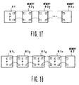
- Fig. 17 shows a first modification of the ninth embodiment of the semiconductor integrated circuit device according to the present invention.
- This first modification is of single CPU semiconductor integrated circuit device, in which a semiconductor chip 81 having a CPU and a plurality of memories 82 1 , ..., 82 n are arranged adjacent to each other in a line and further connected to each other by boding wires, respectively.
- the power consumption can be reduced, and further a large amount of data can be accessed by the CPU at high speed.
- Fig. 18 shows a second modification of the ninth embodiment of the semiconductor integrated circuit device according to the present invention.
- This second modification is of multi-CPU semiconductor integrated circuit device, in which a plurality of semiconductor chips 81 1 , .., 81 n each including a CPU and a memory 82 are arranged adjacent to each other in a line and further connected to each other by boding wires.
- the construction of the small-amplitude input/output circuits 91 and 94 is the same as that of the small-amplitude input/output circuit 87 shown in Fig. 15A.
- the small-amplitude signal transmitted from the adjacent semiconductor chip via the bonding wire 98 is detected by the small-amplitude input/output circuit 91, converted into a large-amplitude signal vibrating between the drive voltage V DD and the ground voltage GND, for instance, and then transmitted to the selector 92 a . Further, on the basis of the control signal (not shown) applied to the selector 92a, the large-amplitude signal is selectively transmitted through the selector 92a to the function block 93 or bypassed to the small-amplitude input/output circuit 94 via the bus 92c and the selector 92b.
- the large-amplitude signal transmitted to the small-amplitude input/output circuit 94 is converted into a small-amplitude signal by the small-amplitude input/output circuit 94, and then transmitted to the adjacent semiconductor chip via the pad 96 and the bonding wire 99.
- the small-amplitude signal transmitted from the adjacent semiconductor chip via the bonding wire 99 is detected and further converted into a large-amplitude signal by the small-amplitude input/output circuit 94 and then transmitted to the selector 92b. Further, on the basis of the control signal (not shown) applied to the selector 92b, the large-amplitude signal is selectively transmitted through the selector 92b to the function block 93 or bypassed to the small-amplitude input/output circuit 91 via the bus 92c and the selector 92a. The large-amplitude signal transmitted to the small-amplitude input/output circuit 91 is converted into a small-amplitude signal, and then transmitted to the adjacent semiconductor chip via the pad 95 and the bonding wire 98.
- the transmitted signals are of small-amplitude signal, it is possible to reduce the power consumption of the driver circuits of the small-amplitude input/output circuits, respectively, with the result that the semiconductor integrated circuit device can be minimized.
- Fig. 20 shows an eleventh embodiment of the semiconductor integrated circuit device according to the present invention.
- This embodiment is different from the tenth embodiment shown in Fig. 19 in that two small-amplitude input/output circuits 110 and 111 are additionally connected on both ends of the bypassing bus 92c.
- This embodiment is effective when the capacitance of the bypass 92C is large. In this construction, it is of course possible to reduce the power consumption of the semiconductor integrated circuit device.
- Fig. 21 shows a twelfth embodiment of the semiconductor integrated circuit device according to the present invention.
- four semiconductor chips 120 11 , 120 12 , 120 13 , and 120 22 are arranged in a matrix pattern and further connected to each other by bonding wires.
- each semiconductor chip is composed of the two small-amplitude input/output circuits 91 and 94, the switch circuit 92, the function block 93, and the two pads 95 and 96. Therefore, since the signals transmitted between the semiconductor chips are of small-amplitude signal, it is possible to reduce the power of the driver circuit of the small-amplitude input/output circuit and thereby to minimize the power consumption thereof.
- Fig. 22 shows a thirteenth embodiment of the semiconductor integrated circuit device according to the present invention.
- a plurality of semiconductor chips 130 11 , 130 12 , ..., 130 mn arranged in a matrix pattern (m x n units) are connected to each other by bonding wires.
- each of the four corner semiconductor chips 130 11 , 130 1n , 130 m1 and 130 mn arranged at four corners of the matrix pattern is constructed as shown in Fig. 15B.
- each of the semiconductor chips comprises three small-amplitude input/output circuits 151, 152 and 153; a switch circuit 155, a function block 156, three pads 157 1 , 157 2 and 157 3 .
- the pad 157 1 is connected to the small-amplitude input/output circuit 151; the pad 157 2 is connected to the small-amplitude input/output circuit 152; and the pad 157 3 is connected to the small-amplitude input/output circuit 153.
- the small-amplitude signals each transmitted from each adjacent semiconductor chip via each of the pads 157 i is detected by each of the small-amplitude input/output circuits 151, 152 and 153, converted into a large-amplitude signal vibrating between the drive voltage V DD and the ground voltage GND, for instance, and then transmitted to the switch circuit 155. Further, on the basis of the control signal (not shown) applied to the switch circuit 155, the large-amplitude signal is selectively transmitted through the switch circuit 155 to the function block 156 or bypassed to the other small-amplitude input/output circuit. The large-amplitude signal transmitted to the small-amplitude input/output circuit is converted into a small-amplitude signal, and then transmitted to the adjacent semiconductor chip via the corresponding pad and
- the large-amplitude signal is transmitted to the function block 156, the transmitted large-amplitude signal is processed.
- the output of the function block 156 is transmitted to the small-amplitude input/output circuit via the switch circuit, converted into a small-amplitude signal, and then transmitted to the adjacent semiconductor chip via the corresponding pad.
- the pad 147 1 is connected to the small-amplitude input/output circuit 141 and further connected to the adjacent semiconductor chip via a bonding wire; the pad 147 2 is connected to the small-amplitude input/output circuit 142 and further connected to the adjacent semiconductor chip via a bonding wire; the pad 147 3 is connected to the small-amplitude input/output circuit 143 and further connected to the adjacent semiconductor chip via a bonding wire; and the pad 147 4 is connected to the small-amplitude input/output circuit 144 and further connected to the adjacent semiconductor chip via a bonding wire.
- the small-amplitude signal transmitted from the adjacent semiconductor chip via the pads is detected and further converted into a large-amplitude signal and then transmitted to the switch circuit 145. Further, on the basis of the control signal (not shown) applied to the switch circuit 145, the large-amplitude signal is selectively transmitted through the switch circuit 145 to the function block 146 or bypassed to the other small-amplitude input/output circuit. The large-amplitude signal transmitted to the small-amplitude input/output circuit is converted into a small-amplitude signal, and then transmitted to the adjacent semiconductor chip via the corresponding pad and bonding wire.
- the transmitted large-amplitude signal is processed.
- the output of the function block 146 is transmitted to the small-amplitude input/output circuit via the switch circuit 145, converted into a small-amplitude signal, and then transmitted to the adjacent semiconductor chip via the corresponding pad.
- the signal transmitted between the chips is of small-amplitude signal, it is possible to reduce the power of the driver circuits of the small-amplitude input/output circuits, respectively, with the result that the power consumption of the semiconductor integrated circuit device can be minimized.
- the chips are connected by use of bonding wires, it is also possible to connect these chips directly by use of substrate wires.
- pads 161a, 161b, 161c and 161d are formed on a package substrate 160; and further bumps 162a, 162b, 162c and 162d are formed on these pads, respectively.
- the pad 161a and the pad 161c are connected to each other by a substrate wire 165a, and the pad 161b and the pad 161d are connected to each other by a substrate wire 165b. Further, pads 171a and 171b are formed on the surface of a semiconductor chip 171, and pads 172a and 172b are formed on the surface of another semiconductor chip 172.
- the pads 171a and 171b formed on the semiconductor chip 171 are connected to the pads 161a and 161b formed on the package substrate 160 via the bumps 162a and 162b, respectively; and the pads 172a and 172b formed on the semiconductor chip 172 are connected to the pads 161c and 161d formed on the package substrate 160 via the bumps 162c and 162d, respectively.
- Fig. 25 shows a fourteenth embodiment of the semiconductor integrated circuit device according to the present invention, in which a plurality of semiconductor chips 180 1 , .., 180 n arranged in a line on the same plane are connected to each other through two buses 186 and 187.
- the semiconductor chip 180 1 is provided with a small-amplitude output circuit composed of the bias circuit 1 A and the driver circuit 5 A , and the small-amplitude input circuit composed of the voltage divider circuit 9 A and the receiver circuit 10 A , in the same way as with the case of the semiconductor chip A of the seventh embodiment shown in Fig. 12.
- the output terminal of the voltage divider circuit 9 A is connected to the pad 182 1
- the output terminal of the driver circuit 5 A is connected to the pad 183 1 .
- the other semiconductor chips 180 i are provided with a small-amplitude output circuit composed of the driver circuit 5 B , and the small-amplitude input circuit composed of the voltage divider circuit 9 B and the receiver circuit 10 B , respectively, in the same way as with the case of the semiconductor chip B of the seventh embodiment shown in Fig. 12.
- the output terminal of the voltage divider circuit 9 B is connected to the pad 182 i
- the output terminal of the driver circuit 5 B is connected to the pad 183 i .
- the signals transferred between the semiconductor chips are of small-amplitude signal, in the same way as with the case of the seventh embodiment, it is possible to reduce the power of the driver circuits, so that the power consumption thereof can be minimized.
- the semiconductor chips are connected through the two buses, it is possible to transmit signals at a high speed by a small power. Further, signals transmitted from one chip can be received by the other chips at the same time.
- Fig. 26 shows a fifteenth embodiment of the semiconductor integrated circuit device according to the present invention, in which a plurality of the semiconductor chips 180 1 , .., 180 n arranged in the fourteenth embodiment shown in Fig. 25 are laminated one upon another. This structure is referred to as a multi-chip semiconductor device.
- the buses 186 and 187 are constructed by junction wires for connecting the respective chips.
- the bias circuit on the other semiconductor chip 180 i (i ⁇ 1) on which no bias circuit is provided.
- the pads 182 1 , .., 182 n and the bus 186 can be eliminated.
- one of the two output ends of the driver circuit 5 A is connected to the pad 182 i , and the other of the two output ends thereof is connected to the pad 183 i .
- the bias circuit is constructed by the N-channel transistors, it is of course possible to construct the bias circuit by use of P-channel transistors. In this case, the drive voltage V DD and the ground voltage GND must be reversed with respect to each other.
- the signals flowing through the transfer path are of small-amplitude signal
- the power of the driver circuits for driving the transfer path can be reduced, with the result that the power consumption of the semiconductor integrated circuit can be minimized.
Landscapes
- Engineering & Computer Science (AREA)
- Computer Hardware Design (AREA)
- Physics & Mathematics (AREA)
- Computing Systems (AREA)
- General Engineering & Computer Science (AREA)
- Mathematical Physics (AREA)
- Logic Circuits (AREA)
- Semiconductor Integrated Circuits (AREA)
- Dc Digital Transmission (AREA)
- Memory System (AREA)
- Dram (AREA)
- Amplifiers (AREA)
Applications Claiming Priority (4)
| Application Number | Priority Date | Filing Date | Title |
|---|---|---|---|
| JP132826/96 | 1996-04-30 | ||
| JP13282696 | 1996-04-30 | ||
| JP87963/97 | 1997-04-07 | ||
| JP8796397A JP3195913B2 (ja) | 1996-04-30 | 1997-04-07 | 半導体集積回路装置 |
Publications (2)
| Publication Number | Publication Date |
|---|---|
| EP0805557A2 true EP0805557A2 (de) | 1997-11-05 |
| EP0805557A3 EP0805557A3 (de) | 1999-04-07 |
Family
ID=26429188
Family Applications (1)
| Application Number | Title | Priority Date | Filing Date |
|---|---|---|---|
| EP19970107187 Withdrawn EP0805557A3 (de) | 1996-04-30 | 1997-04-30 | Vorrichtung mit integrierter Halbleiterschaltung |
Country Status (3)
| Country | Link |
|---|---|
| US (2) | US5933029A (de) |
| EP (1) | EP0805557A3 (de) |
| JP (1) | JP3195913B2 (de) |
Cited By (1)
| Publication number | Priority date | Publication date | Assignee | Title |
|---|---|---|---|---|
| EP1024598A1 (de) * | 1999-01-29 | 2000-08-02 | Fairchild Semiconductor Corporation | CMOS-ECL Umsetzer mit hoher Geschwindigkeit und geringer Phasenverschiebung |
Families Citing this family (23)
| Publication number | Priority date | Publication date | Assignee | Title |
|---|---|---|---|---|
| US6133749A (en) * | 1999-01-04 | 2000-10-17 | International Business Machines Corporation | Variable impedance output driver circuit using analog biases to match driver output impedance to load input impedance |
| US6400178B1 (en) * | 2000-05-30 | 2002-06-04 | International Business Machines Corporation | CMOS small signal terminated receiver |
| JP2002354134A (ja) * | 2001-05-23 | 2002-12-06 | Aiphone Co Ltd | 集合住宅インターホンシステム |
| US7305310B2 (en) * | 2004-10-18 | 2007-12-04 | Electro Industries/Gauge Tech. | System and method for compensating for potential and current transformers in energy meters |
| US7508190B2 (en) * | 2004-10-20 | 2009-03-24 | Electro Industries/Gauge Tech. | Test pulses for enabling revenue testable panel meters |
| US9080894B2 (en) | 2004-10-20 | 2015-07-14 | Electro Industries/Gauge Tech | Intelligent electronic device for receiving and sending data at high speeds over a network |
| US7304586B2 (en) | 2004-10-20 | 2007-12-04 | Electro Industries / Gauge Tech | On-line web accessed energy meter |
| US7747733B2 (en) | 2004-10-25 | 2010-06-29 | Electro Industries/Gauge Tech | Power meter having multiple ethernet ports |
| US8190381B2 (en) | 2005-01-27 | 2012-05-29 | Electro Industries/Gauge Tech | Intelligent electronic device with enhanced power quality monitoring and communications capabilities |
| US8620608B2 (en) | 2005-01-27 | 2013-12-31 | Electro Industries/Gauge Tech | Intelligent electronic device and method thereof |
| US8160824B2 (en) | 2005-01-27 | 2012-04-17 | Electro Industries/Gauge Tech | Intelligent electronic device with enhanced power quality monitoring and communication capabilities |
| US7996171B2 (en) | 2005-01-27 | 2011-08-09 | Electro Industries/Gauge Tech | Intelligent electronic device with broad-range high accuracy |
| JP5020625B2 (ja) * | 2006-12-22 | 2012-09-05 | キヤノン株式会社 | インタフェース回路 |
| US7920976B2 (en) | 2007-03-27 | 2011-04-05 | Electro Industries / Gauge Tech. | Averaging in an intelligent electronic device |
| US20130275066A1 (en) | 2007-04-03 | 2013-10-17 | Electro Industries/Gaugetech | Digital power metering system |
| US9989618B2 (en) | 2007-04-03 | 2018-06-05 | Electro Industries/Gaugetech | Intelligent electronic device with constant calibration capabilities for high accuracy measurements |
| US11307227B2 (en) | 2007-04-03 | 2022-04-19 | Electro Industries/Gauge Tech | High speed digital transient waveform detection system and method for use in an intelligent electronic device |
| US10845399B2 (en) | 2007-04-03 | 2020-11-24 | Electro Industries/Gaugetech | System and method for performing data transfers in an intelligent electronic device |
| JP5040421B2 (ja) * | 2007-05-07 | 2012-10-03 | 富士通セミコンダクター株式会社 | 定電圧回路、定電圧供給システム、および定電圧供給方法 |
| US12061218B2 (en) | 2008-03-13 | 2024-08-13 | Ei Electronics Llc | System and method for multi-rate concurrent waveform capture and storage for power quality metering |
| KR20120050262A (ko) | 2010-11-10 | 2012-05-18 | 삼성전자주식회사 | 소스 팔로워 타입 전압 모드 전송기 및 그에 따른 구동 전압 제어방법 |
| US12433850B2 (en) | 2016-05-05 | 2025-10-07 | Aquestive Therapeutics, Inc. | Enhanced delivery epinephrine and prodrug compositions |
| US12427121B2 (en) | 2016-05-05 | 2025-09-30 | Aquestive Therapeutics, Inc. | Enhanced delivery epinephrine compositions |
Citations (1)
| Publication number | Priority date | Publication date | Assignee | Title |
|---|---|---|---|---|
| EP0608786A1 (de) * | 1993-01-25 | 1994-08-03 | Standard Microsystems Corporation | Übermittlung von logischen Signalen sehr niedriger Spannung zwischen CMOS-Chips für eine grosse Anzahl Hochgeschwindigkeitsausgangsleitungen mit jeweils grosser kapazitiver Last |
Family Cites Families (17)
| Publication number | Priority date | Publication date | Assignee | Title |
|---|---|---|---|---|
| GB1245347A (en) * | 1968-07-01 | 1971-09-08 | Nippon Telegraph & Telephone | Improved high speed logic circuit device |
| US3648065A (en) * | 1970-01-28 | 1972-03-07 | Ibm | Storage circuit for shift register |
| JPS593950A (ja) * | 1982-06-30 | 1984-01-10 | Fujitsu Ltd | ゲ−トアレイチツプ |
| JPS60694A (ja) * | 1983-06-15 | 1985-01-05 | Hitachi Ltd | 半導体メモリ |
| US5086238A (en) * | 1985-07-22 | 1992-02-04 | Hitachi, Ltd. | Semiconductor supply incorporating internal power supply for compensating for deviation in operating condition and fabrication process conditions |
| JP2902016B2 (ja) * | 1989-11-21 | 1999-06-07 | 株式会社日立製作所 | 信号伝送方法および回路 |
| EP0432280A1 (de) * | 1989-12-04 | 1991-06-19 | Siemens Aktiengesellschaft | Schnittstelle zwischen zwei an unterschiedlichen Betriebsspannungen betriebenen elektrischen Schaltungen |
| CA2062414C (en) * | 1991-03-07 | 1999-03-30 | Satomi Horita | A circuit for interconnecting integrated semiconductor circuits |
| JPH04360312A (ja) * | 1991-06-06 | 1992-12-14 | Hitachi Ltd | 半導体集積回路装置と信号処理装置 |
| US5369317A (en) * | 1992-06-26 | 1994-11-29 | Micron Technology, Inc. | Circuit and method for controlling the potential of a digit line and in limiting said potential to a maximum value |
| US5459412A (en) * | 1993-07-01 | 1995-10-17 | National Semiconductor Corporation | BiCMOS circuit for translation of ECL logic levels to MOS logic levels |
| US5644245A (en) * | 1993-11-24 | 1997-07-01 | Tokyo Electron Limited | Probe apparatus for inspecting electrical characteristics of a microelectronic element |
| EP0655839B1 (de) * | 1993-11-29 | 2007-01-03 | Fujitsu Limited | Elektronisches System zum Abschluss von Busleitungen |
| JPH07302144A (ja) * | 1994-05-02 | 1995-11-14 | Hitachi Ltd | インタフェース回路 |
| US5510729A (en) * | 1995-03-27 | 1996-04-23 | General Datacomm, Inc. | Output characteristics stabilization of CMOS devices |
| US5585744A (en) * | 1995-10-13 | 1996-12-17 | Cirrus Logic, Inc. | Circuits systems and methods for reducing power loss during transfer of data across a conductive line |
| US5886539A (en) * | 1997-04-10 | 1999-03-23 | Advanced Micro Devices, Ind | Communication within an integrated circuit by data serialization through a metal plane |
-
1997
- 1997-04-07 JP JP8796397A patent/JP3195913B2/ja not_active Expired - Fee Related
- 1997-04-28 US US08/848,126 patent/US5933029A/en not_active Expired - Lifetime
- 1997-04-30 EP EP19970107187 patent/EP0805557A3/de not_active Withdrawn
-
1999
- 1999-03-29 US US09/280,726 patent/US6037805A/en not_active Expired - Lifetime
Patent Citations (1)
| Publication number | Priority date | Publication date | Assignee | Title |
|---|---|---|---|---|
| EP0608786A1 (de) * | 1993-01-25 | 1994-08-03 | Standard Microsystems Corporation | Übermittlung von logischen Signalen sehr niedriger Spannung zwischen CMOS-Chips für eine grosse Anzahl Hochgeschwindigkeitsausgangsleitungen mit jeweils grosser kapazitiver Last |
Cited By (2)
| Publication number | Priority date | Publication date | Assignee | Title |
|---|---|---|---|---|
| EP1024598A1 (de) * | 1999-01-29 | 2000-08-02 | Fairchild Semiconductor Corporation | CMOS-ECL Umsetzer mit hoher Geschwindigkeit und geringer Phasenverschiebung |
| US6175249B1 (en) | 1999-01-29 | 2001-01-16 | Fairchild Semiconductor Corp. | High speed low skew CMOS to ECL converter |
Also Published As
| Publication number | Publication date |
|---|---|
| US6037805A (en) | 2000-03-14 |
| JP3195913B2 (ja) | 2001-08-06 |
| US5933029A (en) | 1999-08-03 |
| EP0805557A3 (de) | 1999-04-07 |
| JPH1022812A (ja) | 1998-01-23 |
Similar Documents
| Publication | Publication Date | Title |
|---|---|---|
| US5933029A (en) | Semiconductor integrated circuit device comprising a bias circuit, a driver circuit, and a receiver circuit | |
| JP3562725B2 (ja) | 出力バッファ回路、および入出力バッファ回路 | |
| US5483110A (en) | Signal transmission method, signal transmission circuit and information processing system using same | |
| US5283565A (en) | Multimode input circuit receiving two signals having amplitude variations different from each other | |
| US5461333A (en) | Multi-chip modules having chip-to-chip interconnections with reduced signal voltage level and swing | |
| US7078934B2 (en) | Level conversion circuit | |
| US5825214A (en) | Integrated circuit arrangement with diode characteristic | |
| GB2248988A (en) | Interface circuits | |
| US5455524A (en) | CMOS integrated circuit device and data processing system using the same | |
| US4583013A (en) | Oscillator signal detect circuit | |
| JP3315286B2 (ja) | パルス倍電圧回路 | |
| JPH0671202B2 (ja) | 液晶駆動装置 | |
| KR950016000A (ko) | 씨모스(cmos) 회로와 바이폴라 회로가 혼재되어 있는 반도체 디바이스 | |
| US6417655B2 (en) | Common mode bias voltage generator | |
| US5701072A (en) | Integrated circuit output driver systems including multiple power and ground lines | |
| KR100249974B1 (ko) | 반도체 집적회로 장치 | |
| JP3233627B2 (ja) | 半導体装置 | |
| JP2690060B2 (ja) | 半導体回路 | |
| JPH06291638A (ja) | 半導体装置 | |
| US5233235A (en) | On-chip intermediate driver for discrete WSI systems | |
| EP0548551A1 (de) | Logische Schaltung mit hoher Geschwindigkeit und geringem Leistungsverbrauch | |
| US20040165471A1 (en) | Semiconductor device | |
| JPH05327465A (ja) | 半導体集積回路 | |
| US6806735B2 (en) | Buffer for contact circuit | |
| KR970012784A (ko) | 노말/테스트 겸용 본딩 패드를 가진 반도체 메모리 장치 |
Legal Events
| Date | Code | Title | Description |
|---|---|---|---|
| PUAI | Public reference made under article 153(3) epc to a published international application that has entered the european phase |
Free format text: ORIGINAL CODE: 0009012 |
|
| 17P | Request for examination filed |
Effective date: 19970430 |
|
| AK | Designated contracting states |
Kind code of ref document: A2 Designated state(s): DE FR GB |
|
| PUAL | Search report despatched |
Free format text: ORIGINAL CODE: 0009013 |
|
| AK | Designated contracting states |
Kind code of ref document: A3 Designated state(s): DE FR GB |
|
| 17Q | First examination report despatched |
Effective date: 20020620 |
|
| STAA | Information on the status of an ep patent application or granted ep patent |
Free format text: STATUS: THE APPLICATION IS DEEMED TO BE WITHDRAWN |
|
| 18D | Application deemed to be withdrawn |
Effective date: 20040914 |