EP0805557A2 - Semiconductor integrated circuit device - Google Patents
Semiconductor integrated circuit device Download PDFInfo
- Publication number
- EP0805557A2 EP0805557A2 EP19970107187 EP97107187A EP0805557A2 EP 0805557 A2 EP0805557 A2 EP 0805557A2 EP 19970107187 EP19970107187 EP 19970107187 EP 97107187 A EP97107187 A EP 97107187A EP 0805557 A2 EP0805557 A2 EP 0805557A2
- Authority
- EP
- European Patent Office
- Prior art keywords
- signal
- circuit
- output
- amplitude
- input
- Prior art date
- Legal status (The legal status is an assumption and is not a legal conclusion. Google has not performed a legal analysis and makes no representation as to the accuracy of the status listed.)
- Withdrawn
Links
Images


Classifications
-
- H—ELECTRICITY
- H10—SEMICONDUCTOR DEVICES; ELECTRIC SOLID-STATE DEVICES NOT OTHERWISE PROVIDED FOR
- H10D—INORGANIC ELECTRIC SEMICONDUCTOR DEVICES
- H10D89/00—Aspects of integrated devices not covered by groups H10D84/00 - H10D88/00
- H10D89/211—Design considerations for internal polarisation
- H10D89/213—Design considerations for internal polarisation in field-effect devices
-
- H—ELECTRICITY
- H03—ELECTRONIC CIRCUITRY
- H03K—PULSE TECHNIQUE
- H03K19/00—Logic circuits, i.e. having at least two inputs acting on one output; Inverting circuits
- H03K19/003—Modifications for increasing the reliability for protection
- H03K19/00369—Modifications for compensating variations of temperature, supply voltage or other physical parameters
- H03K19/00384—Modifications for compensating variations of temperature, supply voltage or other physical parameters in field effect transistor circuits
-
- H—ELECTRICITY
- H03—ELECTRONIC CIRCUITRY
- H03K—PULSE TECHNIQUE
- H03K19/00—Logic circuits, i.e. having at least two inputs acting on one output; Inverting circuits
- H03K19/0175—Coupling arrangements; Interface arrangements
- H03K19/0185—Coupling arrangements; Interface arrangements using field effect transistors only
- H03K19/018507—Interface arrangements
-
- H—ELECTRICITY
- H10—SEMICONDUCTOR DEVICES; ELECTRIC SOLID-STATE DEVICES NOT OTHERWISE PROVIDED FOR
- H10W—GENERIC PACKAGES, INTERCONNECTIONS, CONNECTORS OR OTHER CONSTRUCTIONAL DETAILS OF DEVICES COVERED BY CLASS H10
- H10W72/00—Interconnections or connectors in packages
- H10W72/50—Bond wires
- H10W72/541—Dispositions of bond wires
- H10W72/5445—Dispositions of bond wires being orthogonal to a side surface of the chip, e.g. parallel arrangements
-
- H—ELECTRICITY
- H10—SEMICONDUCTOR DEVICES; ELECTRIC SOLID-STATE DEVICES NOT OTHERWISE PROVIDED FOR
- H10W—GENERIC PACKAGES, INTERCONNECTIONS, CONNECTORS OR OTHER CONSTRUCTIONAL DETAILS OF DEVICES COVERED BY CLASS H10
- H10W72/00—Interconnections or connectors in packages
- H10W72/90—Bond pads, in general
- H10W72/931—Shapes of bond pads
- H10W72/932—Plan-view shape, i.e. in top view
-
- H—ELECTRICITY
- H10—SEMICONDUCTOR DEVICES; ELECTRIC SOLID-STATE DEVICES NOT OTHERWISE PROVIDED FOR
- H10W—GENERIC PACKAGES, INTERCONNECTIONS, CONNECTORS OR OTHER CONSTRUCTIONAL DETAILS OF DEVICES COVERED BY CLASS H10
- H10W90/00—Package configurations
- H10W90/701—Package configurations characterised by the relative positions of pads or connectors relative to package parts
- H10W90/751—Package configurations characterised by the relative positions of pads or connectors relative to package parts of bond wires
- H10W90/753—Package configurations characterised by the relative positions of pads or connectors relative to package parts of bond wires between laterally-adjacent chips
Definitions
- the present invention relates to a semiconductor integrated circuit device having driver circuits each for driving a bus, a clock line or an input/output line of a semiconductor chip.
- one of the methods of reducing the power consumption is to reduce the signal amplitude.
- this method is not easy. The reasons are as follows: first, it is difficult to realize the driver circuit for outputting a small amplitude signal under a low power consumption. Or else, it is difficult to realize a receiver circuit for receiving the small-amplitude signal and returning the received small-amplitude signal to the ordinary amplitude signal under a low power consumption.
- the small-amplitude signals have been so far used for only a part of the circuits whose characteristics are well known (e.g., as with the case of bit line signals of a memory device).
- the signals having an amplitude changing between the supply voltage and the ground voltage have been so far used.
- the power consumption cannot be reduced in the semiconductor integrated circuit device having the driver circuits.
- a first aspect of the present invention provides a semiconductor integrated circuit device, comprising: a bias circuit for generating a predetermined voltage fixed between a first supply voltage and a second supply voltage; a driver circuit for receiving an inversion input signal and a non-inversion input signal each vibrating between the first and second supply voltages, for converting the received input signals into a signal vibrating between an output voltage of said bias circuit and the first supply voltage, and for driving a transfer path by the converted signal; a voltage divider circuit for dividing an output voltage of said bias circuit; and a receiver circuit for detecting the signal for driving the transfer path by use of an output of said voltage divider circuit as a reference voltage, and for converting the detected signal into a signal vibrating between the first supply voltage and the second supply voltage.
- a second aspect of the present invention provides a semiconductor integrated circuit device, comprising: a bias circuit for generating a predetermined voltage fixed between a first supply voltage and a second supply voltage; a driver circuit for receiving an inversion input signal and a non-inversion input signal each vibrating between the first and second supply voltages, for converting the received input signals into a signal vibrating between an output voltage of said bias circuit and the first supply voltage on the basis of an enable signal, and for driving a transfer path by the converted signal or for setting an output thereof to a high impedance; a voltage divider circuit for dividing an output voltage of said bias circuit; and a receiver circuit for detecting the signal for driving the transfer path by use of an output of said voltage divider circuit as a reference voltage, and for converting the detected signal into a signal vibrating between the first supply voltage and the second supply voltage.
- a third aspect of the present invention provides a semiconductor integrated circuit device, comprising: a bias circuit for generating a predetermined voltage fixed between a first supply voltage and a second supply voltage; a driver circuit for receiving an inversion input signal and a non-inversion input signal each vibrating between the first and second supply voltages, for converting the received input signals into two differential signals each vibrating between an output voltage of said bias circuit and the first supply voltage, and for driving two transfer paths by the two differential signals, respectively; and a receiver circuit for detecting the differential signals for driving the transfer paths, and for converting the detected differential signals into a signal vibrating between the first supply voltage and the second supply voltage.
- a fourth aspect of the present invention provides a semiconductor integrated circuit device, comprising: a bias circuit for generating a predetermined voltage fixed between a first supply voltage and a second supply voltage; a driver circuit for receiving an inversion input signal and a non-inversion input signal each vibrating between the first and second supply voltages, for converting the received input signals into two differential signals each vibrating between an output voltage of said bias circuit and the first supply voltage on the basis of an enable signal, and for driving two transfer paths by the two differential signals or for setting two outputs thereof to a high impedance, respectively; and a receiver circuit for detecting the differential signals for driving the transfer paths, and for converting the detected differential signals into a signal vibrating between the first supply voltage and the second supply voltage.
- a fifth aspect of the present invention provides a semiconductor integrated circuit device, comprising: a first semiconductor chip including: a bias circuit for generating a predetermined voltage fixed between a first supply voltage and a second supply voltage; a first driver circuit for receiving a first inversion input signal and a first non-inversion input signal each vibrating between the first and second supply voltages, for converting the received input signals into a signal vibrating between an output voltage of said bias circuit and the first supply voltage on the basis of a first enable signal, and for outputting the converted signal or for setting an output thereof to a high impedance; a first voltage divider circuit for dividing an output voltage of said bias circuit; and a first receiver circuit; and a second semiconductor chip including: a second voltage divider circuit having an input end connected to an input end of said first voltage divider circuit via a wire, for dividing an output voltage of said bias circuit; a second driver circuit having an output end connected to an output end of said first driver circuit via a transfer wire, for receiving a second inversion input signal and
- a sixth aspect of the present invention provides a semiconductor integrated circuit device, comprising: a first semiconductor chip including: a first bias circuit for generating a predetermined fixed voltage between a first supply voltage and a second supply voltage; a first driver circuit for receiving a first inversion input signal and a first non-inversion input signal each vibrating between the first and second supply voltages, for converting the received input signals into two differential signals each vibrating between an output voltage of said first bias circuit and the first supply voltage on the basis of a first enable signal, and for outputting the converted differential signals or setting two outputs thereof to a high impedance, respectively; and a first receiver circuit; and a second semiconductor chip including: a second bias circuit for generating another predetermined voltage fixed between a third supply voltage and a fourth supply voltage; a second driver circuit for receiving a second inversion input signal and a second non-inversion input signal each vibrating between the third and fourth supply voltages, for converting the received input signals into two differential signals each vibrating between an output voltage of said second bias circuit and the
- a seventh aspect of the present invention provides a semiconductor integrated circuit device, which comprises: a plurality of semiconductor chips arranged in a matrix pattern, each semiconductor chip including: input/output ends connected to input/output ends of another adjacent semiconductor chip by transfer wires of bonding wires or substrate wires, respectively, for transferring data; and a small-amplitude input/output circuit arranged in each of the input/output ends of a part or all of said semiconductor chips, for receiving a non-inversion signal and an inversion signal each vibrating between a first supply voltage and a second supply voltage according to each semiconductor chip including the small-amplitude input/output circuit, for converting the received signals into a small-amplitude signal vibrating between a predetermined voltage fixed between the first and second supply voltages and the first supply voltage, for outputting the converted signal to the input/output end of another adjacent semiconductor chip via the transfer wire, and for converting the small-amplitude signal transferred via the transfer wire into a signal vibrating between the first supply voltage and the second supply voltage.
- Fig. 1 shows a first embodiment thereof, which comprises a small-amplitude output circuit having a bias circuit 1 and a driver circuit 5, a voltage divider circuit 9, and a receiver circuit 10 having a sense amplifier circuit.
- the bias circuit 1 generates a predetermined voltage, which comprises a current source 2, a series circuit constructed by connecting an n-units of N-channel MOS transistors M 1 , M 2 , ..., M n of the same size in series, an N-channel MOS transistor 3, and a capacitor 4.
- a current source 2 a series circuit constructed by connecting an n-units of N-channel MOS transistors M 1 , M 2 , ..., M n of the same size in series, an N-channel MOS transistor 3, and a capacitor 4.
- the drain terminal of the transistor M n is connected to an output terminal of the current source 2; and the source terminal of the transistor M 1 is grounded.
- the drain terminal of the transistor 3 is connected to a drive voltage supply V DD ; the gate terminal thereof is connected to the drain terminal of the transistor M n ; and the source terminal thereof is grounded via the capacitor 4.
- the voltage at the drain terminal of the transistor M n is n ⁇ V th .
- the threshold voltage of the transistor 3 can be set to V th
- the voltage at the source terminal of the transistor 3; that is, the voltage at the output terminal N V of the bias circuit 1 can be set to a constant voltage of (n-1) ⁇ V th .
- the capacitor 4 when the capacitor 4 is connected to stabilize the voltage at the output terminal of the bias circuit 1, it is possible to improve the transient response of the output of the driver circuit 1. However, this capacitor 4 can be omitted.
- the driver circuit 5 receives a non-inversion input signal and an inversion input signal both vibrating between the drive voltage V DD and the ground voltage GND, converts the received input signals into a small-amplitude signal vibrating between the output voltage of the bias circuit 1 and the ground voltage GND, and drives a transfer path 100 such as a bus, a clock line, etc. on the basis of the converted small-amplitude signal.
- the driver circuit 5 comprises two series-connected N-channel MOS transistors 6 1 and 6 2 .
- the drain of the transistor 6 1 is connected to the output terminal N V of the bias circuit; the source thereof is connected to the drain of the transistor 6 2 ; and the gate thereof receives a non-inversion input signal. Further, the source of the transistor 6 2 is grounded; and the gate thereof receives an inversion input signal. Further, an output signal of the driver circuit 5 is outputted from a junction point between the two transistors 6 1 and 6 2 to the transfer path 100.
- the voltage divider circuit 9 divides the output voltage of the bias circuit 1, which can be constructed by a plurality of series-connected resistors (e.g., R 1 and R 2 as shown in Fig. 3).
- the receiver circuit 10 detects the small-amplitude signal transmitted through the transfer path 100 by a sense amplifier circuit by use of the output voltage of the voltage divider circuit 9 as a reference voltage, and converts the detected small-amplitude signal into a signal vibrating between the drive voltage V DD and the ground voltage GND.
- the power consumption of the driver circuit is proportional to the amplitude of the output signal. Therefore, the power consumption of this first embodiment can be reduced in comparison with that of the prior art semiconductor integrated circuit device.
- the series-connected circuit thereof can be composed of a plurality of N-channel transistors of different sizes.
- Fig. 2 shows a second embodiment of the semiconductor integrated circuit device according to the present invention, which is different from the first embodiment shown in Fig. 1 in that two NOR gates 7 1 and 7 2 are additionally connected in the driver circuit 5.
- the NOR gate 7 1 executes NOR operation on the basis of the non-inversion input signal and an enable signal, and transmits the operation result to the gate of the transistor 6 1 .
- the NOR gate 7 2 executes NOR operation on the basis of the inversion input signal and the same enable signal, and transmits the operation result to the gate of the transistor 6 2 .
- Fig. 4 shows a third embodiment of the semiconductor integrated circuit device according to the present invention, which is different from the first embodiment shown in Fig. 1 in that the voltage divider circuit 9 is omitted and further two series-connected N-channel MOS transistors 6 3 and 6 4 are additionally connected in the driver circuit 5.
- the drain of the transistor 6 3 is connected to the output terminal of the bias circuit 1; the source thereof is connected to the drain of the transistor 6 4 ; and the gate thereof receives the inversion input signal.
- the source of the transistor 6 4 is grounded; and the gate thereof receives the non-inversion input signal.
- the non-inversion small-amplitude signal can be transmitted from the junction point between the two transistors 6 1 and 6 2 to the receiver circuit 10 via the transfer path 100 1 .
- the inversion small-amplitude signal can be transmitted from the junction point between the two transistors 6 3 and 6 4 to the receiver circuit 10 via the transfer path 100 2 .
- the driver circuit 5 can drive the two transfer paths 100 1 and 100 2 by a differential signal vibrating between a predetermined voltage of (n-1) ⁇ V th and the ground voltage GND. Further, the receiver circuit 10 detects the differential signal transmitted through the two transfer paths 100 1 and 100 2 by the sense amplifier circuit, and further converts the detected differential signal into a signal vibrating between the drive voltage V DD and the ground voltage GND.
- Fig. 5 shows a fourth embodiment of the semiconductor integrated circuit device according to the present invention, which is different from the third embodiment shown in Fig. 4 in that two NOR gates 7 1 and 7 2 are additionally connected in the driver circuit 5.
- the NOR gate 7 1 executes NOR operation on the basis of the non-inversion input signal and an enable signal, and transmits the operation result to the gates of the two transistors 6 1 and 6 4 .
- the NOR gate 7 2 executes NOR operation on the basis of the inversion input signal and the same enable signal, and transmits the operation result to the gates of the two transistor 6 2 and 6 3 .
- the non-inversion input signal and the inversion input signal used in the first to fourth embodiments can be generated by a circuit as shown in Fig. 6.
- the circuit shown in Fig. 6 is composed of two inversion gates 21 and 22, and a transfer gate 23 made up of a P-channel MOS transistor and an N-channel MOS transistor.
- the sense amplifier circuit used for the first to fourth embodiments can be constructed by a circuit as shown in Fig. 7.
- the circuit shown in Fig. 7 is composed of a current source 25, two P-channel MOS transistors 26 1 and 26 2 for receiving a differential input signal, and two N-channel MOS transistors 27 1 and 27 2 .
- the output of the voltage divider circuit 9 is inputted to the gate of the transistor 26 2 .
- the sense amplifier circuit can be constructed as shown in Fig. 8.
- the sense amplifier shown in Fig. 8 is composed of a P-channel MOS transistor 31 for receiving a control signal at the gate thereof; two P-channel MOS transistors 32 1 and 32 2 for receiving a differential input signal at the gate thereof; two common-gate and series-connected P-channel MOS transistor 33 1 and N-channel MOS transistor 34 1 ; and two common-gate and series-connected P-channel MOS transistor 33 2 and N-channel MOS transistor 34 2 .
- Fig. 9 shows a fifth embodiment of the semiconductor integrated circuit device according to the present invention, which is different from the second embodiment shown in Fig. 2 in that a bus terminator circuit 40 is additionally connected between the output terminal of the bias circuit 1 and the transfer path 100.
- This bus terminator circuit 40 can maintain the voltage at the transfer path 100 (e.g., bus) when the output of the driver circuit 5 is set to a high impedance.
- this bus terminator circuit 40 can be constructed by two P-channel MOS transistors 41 1 and 41 2 , and two N-channel MOS transistors 42 1 and 42 2 .
- this third embodiment it is of course possible to obtain the same effect as with the case of the first embodiment and further to minimize the power consumption. Further, it is possible to maintain the voltage at the transfer path 100 (e.g., bus) at a predetermined voltage, when the output of the driver circuit 5 is set to a high impedance.
- the transfer path 100 e.g., bus
- Fig. 11 shows a sixth embodiment of the semiconductor integrated circuit device according to the present invention, which is different from the fourth embodiment shown in Fig. 5 in that a bus terminator circuit 40 is additionally connected between the output terminal of the bias circuit 1 and the two transfer paths 100 1 and 100 2 .
- this bus terminator circuit 40 can maintain the voltages at the two transfer paths 100 1 and 100 2 , respectively when the two outputs of the driver circuit 5 are set to a high impedance, respectively.
- This bus terminator circuit 40 can be constructed as shown in Fig. 10.
- the transfer path 100 1 is connected to the drains of the two transistors 41 1 and 42 1
- the transfer path 100 2 is connected to the drains of the two transistors 41 2 and 42 2 , respectively.
- this sixth embodiment it is possible to minimize the power consumption, as with the case of the fourth embodiment. Further, it is possible to maintain the voltages at the two transfer paths 100 1 and 100 2 at a predetermined voltage, respectively, when the outputs of the driver circuit 5 are set to a high impedance, respectively.
- the driver circuit 5 and the receiver circuit 10 can be driven by the same voltage supply or two different voltage supplies.
- Fig. 12 shows a seventh embodiment of the semiconductor integrated circuit device according to the present invention.
- the semiconductor integrated circuit device comprises two semiconductor chips. Therefore, a bias circuit 1 A , a driver circuit 5 A , a voltage divider circuit 9 A and a receiver circuit 10 A are provided for the semiconductor chip A. Further, a capacitor 4 B , a driver circuit 5 B , a voltage divider circuit 9 B and a receiver circuit 10 B are provided for the semiconductor chip B.
- the bias circuit 1 A the driver circuits 5 A and 5 B , and the voltage divider circuits 9 A and 9 B are the same in construction as the bias circuit 1, the driver circuit 5 and the voltage divider circuit 9 of the second embodiment, respectively.
- the output terminal N V of the bias circuit 1 A is connected to the input terminal of the voltage divider circuit 9 A and further to a pad 51 A formed on the semiconductor chip A. Further, the input terminal of the voltage divider circuit 9 B and one end of the capacitor 4 B are connected to a pad 51 B formed on the chip B. These two chips A and B are arranged at the nearest possible distance and two pads 51 A and 51 B are connected to each other by a boding wire 61. Therefore, the output voltage of the bias circuit 1 A is applied to the voltage divider circuit 9 B and the capacitor 4 B of the chip B via the pad 51 A , the bonding wire 61 and the pad 51 B . Further, the capacitor 4 B is connected to maintain the voltage at the input terminal of the voltage divider circuit 9 B stably. However, this capacitor 4 B can be omitted.
- the output terminal of the driver circuit 5 A is connected to a pad 52 A formed on the chip A
- the output terminal of the driver circuit 5 B is connected to a pad 52 B formed on the chip B.
- These two pads 52 A and 52 B are connected to each other via a bonding wire 62.
- the drain of the transistor 6 1 of the driver circuit 5 B is connected to the pad 51 B .
- the receiver circuit 10 A detects the output of the driver circuit 5 B transmitted through the bonding wire 62 by the sense amplifier circuit by use of the output voltage of the voltage divider circuit 9 A as a reference voltage, and converts the detected output into a signal vibrating between the drive voltage V DD and the ground voltage GND.
- the receiver circuit 10 B detects the output of the driver circuit 5 A transmitted through the bonding wire 62 by the sense amplifier circuit by use of the output voltage of the voltage divider circuit 9 B as a reference voltage, and converts the detected output into a signal vibrating between the drive voltage V DD and the ground voltage GND.
- the driver circuit 5 A when the driver circuit 5 A is being activated, although the receiver circuit 10 B is also activated, the driver circuit 5 B and the receiver circuit 10 A are both deactivated. Further, when the driver circuit 5 B is being activated, although the receiver circuit 10 A is also activated, the driver circuit 5 A and the receiver circuit 10 B are both deactivated. As described above, in this embodiment, since the signal transmitted between the two chips A and B is of small-amplitude signal, it is possible to reduce the power of the driver circuits, respectively, with the result that the power consumption of the semiconductor integrated circuit device can be minimized.
- the small-amplitude output circuit composed of the bias circuit 1 A and the driver circuit 5 A , and the small amplitude input circuit composed of the voltage divider circuit 9 A and the receiver circuit 10 A are provided on the chip A. Further, the small-amplitude output circuit composed of the driver circuit 5 B , and the small amplitude input circuit composed of the voltage divider circuit 9 B and the receiver circuit 10 B are provided on the chip B.
- the output capacitance can be reduced. Further, even if the impedance matching is not considered between the inter-chip bonding wire and the driver circuit, a large signal reflection will not be developed.
- the bias circuit can be formed on the chip B.
- the bonding wire 61 can be eliminated.
- the same voltage supply can be used for both the chips A and B, or else two different voltage supplies can be used for both the chips A and B, respectively.
- the two chips are connected to each other by use of the boding wires, it is also possible to connect the two chips directly by use of wires formed on the substrate.
- Fig. 13 shows an eighth embodiment of the semiconductor integrated circuit device according to the present invention.
- the small-amplitude input circuit and the small-amplitude output circuit are provided for each of the two semiconductor chips A and B arranged at the nearest possible distance.
- the small-amplitude output circuit of the chip A is composed of the bias circuit 1 A and the driver circuit 5 A
- the small-amplitude input circuit of the chip A is composed of the receiver circuit 10 A .
- the small-amplitude output circuit of the chip B is composed of the bias circuit 1 B and the driver circuit 5 B
- the small-amplitude input circuit of the chip B is composed of the receiver circuit 10 B .
- the circuit constructions of the bias circuits 1 A and 1 B and the driver circuits 5 A and 5 B are the same as those of the bias circuit 1 and the driver circuit 5 of the fourth embodiment shown in Fig. 5. Further, the two outputs of the driver circuit 5 A are connected to two pads 53 A and 54 A formed on the chip A, respectively. Further, the two outputs of the driver circuit 5 B are connected to two pads 53 B and 54 B formed on the chip B, respectively.
- the pad 53 A formed on the chip A and the pad 53 B formed on the chip B are connected to each other by a bonding wire 63, and the pad 54 A formed on the chip A and the pad 54 B formed on the chip B are connected to each other by a bonding wire 64.
- the receiver circuit 10 A detects the small-amplitude differential output of the driver circuit 5 B transmitted through the two bonding wires 63 and 64 by the sense amplifier circuit, and converts the detected differential output into a signal vibrating between the drive voltage V DD and the ground voltage GND. Further, the receiver circuit 10 B detects the small-amplitude differential output of the driver circuit 5 A transmitted through the two bonding wires 63 and 64 by the sense amplifier circuit, and converts the detected differential output into a signal vibrating between the drive voltage V DD and the ground voltage GND.
- the driver circuit 5 A when the driver circuit 5 A is being activated, although the receiver circuit 10 B is also activated, the driver circuit 5 B and the receiver circuit 10 A are both deactivated. Further, when the driver circuit 5 B is being activated, although the receiver circuit 10 A is also activated, the driver circuit 5 A and the receiver circuit 10 B are both deactivated.
- the signal transmitted between the two chips A and B is of small-amplitude signal, it is possible to reduce the power of the driver circuits, respectively, with the result that the power consumption of the semiconductor integrated circuit device can be minimized.
- the output capacitance can be reduced. Further, even if the impedance matching is not considered between the interchip bonding wire and the driver circuit, a large signal reflection will not be developed.
- the two chips A and B connected to each other by use of bonding wires can be mounted on the same lead frame base, and then sealed by use of a resin.
- FIG. 14 A ninth embodiment of the semiconductor integrated circuit device according to the present invention will be described hereinbelow with reference to Fig. 14 and Figs. 15A and 15B.
- Fig. 14 is an entire circuit construction of this embodiment, in which a plurality of semiconductor chips 72 1 , ..., 72 n arranged in a line are connected to each other by use of bonding wires 77.
- Each of the semiconductor chips 72 1 and 72 n arranged on both the ends is constructed as a chip 85 shown in Fig. 15A. That is, the end chip 85 is provided with a function block 86, a small-amplitude input/output circuit 87, and a pad 88.
- This small-amplitude input/output circuit 87 is the same as the small-amplitude input circuit and the small-amplitude output circuit of the seventh and eighth embodiments shown in Fig. 12 or Fig. 13, respectively. Further, when the small-amplitude input circuit and the small-amplitude output circuit of the eighth embodiment are used, two pads 88 are necessary.
- the construction of the small-amplitude input/output circuits 91 and 94 is the same as that of the small-amplitude input/output circuit 87 shown in Fig. 15A.
- the output signal of the function block 86 is converted into a small-amplitude signal by the small-amplitude input/output circuit 87, and then transmitted to the adjacent semiconductor chip through the pad 88 and the bonding wire 89. Further, a small-amplitude signal transmitted by the adjacent semiconductor chip through the boding wire 89 is inputted to the small-amplitude input/output circuit 87 via the pad 88, amplified into a large-amplitude signal, and then transmitted to the functional block 86.
- the small-amplitude signal transmitted from the adjacent semiconductor chip via the pad 95 for instance is amplified into a large-amplitude signal by the small-amplitude input/output circuit 91, converted into a large-amplitude signal, and then transmitted to the switch circuit 92.
- the large-amplitude signal is selectively transmitted through the switch circuit 92 to the function block 93 or bypassed to the small-amplitude input/output circuit 94.
- the large-amplitude signal transmitted to the small-amplitude input/output circuit 94 is converted into a small-amplitude signal, and then transmitted to the adjacent semiconductor chip via the pad 96 and the bonding wire 99.
- control signal is transmitted from the other semiconductor chip or the outside of the semiconductor integrated circuit device.
- the transmitted signal is processed.
- the signal is transmitted to the small-amplitude input/output circuit 91 or the small-amplitude input/output circuit 94 via the switch circuit 92.
- the transmitted signal is converted into the small-amplitude signal by the small-amplitude input/output circuit 91 or the small-amplitude input/output circuit 94, and then transmitted to the adjacent semiconductor chip via the bonding wire 98 or the bonding wire 99.
- the function block 86 is a circuit corresponding to a CPU or a memory, which is provided with predetermined processing functions.
- the small-amplitude signal transmitted from the adjacent semiconductor chip via the pad 96 is amplified into a large-amplitude signal by the small-amplitude input/output circuit 94. Further, on the basis of the control signal (not shown) applied to the switch circuit 92, the large-amplitude signal is selectively transmitted through the switch circuit 92 to the function block 93 or bypassed to the small-amplitude input/output circuit 91. The large-amplitude signal transmitted to the small-amplitude input/output circuit 91 is converted into a small-amplitude signal, and then transmitted to the adjacent semiconductor chip via the pad 95 and the bonding wire 98.
- the signal transmitted between the adjacent chips is of small-amplitude signal, it is possible to reduce the power of the driver circuits of the small-amplitude input/output circuits, respectively, with the result that the power consumption of the semiconductor integrated circuit device can be minimized.
- Figs. 16A, 16B and 16C show practical constructions of the switch circuit 92 used for the ninth embodiment of the semiconductor integrated circuit device according to the present invention.
- the switch circuit 92 is composed of three switch elements 101, 102 and 103.
- the switch element 101 connects a node N 1 to a node N 2 on the basis of a control signal S 12 applied to the same switch element 101;
- the switch element 102 connects the node N 2 to a node N 3 on the basis of a control signal S 23 applied to the same switch element 102;
- the switch element 103 connects the node N 3 to the node N 1 on the basis of a control signal S 31 applied to the same switch element 103.
- each switch element is composed of an inverter circuit 105 and a transfer gate having a P-channel MOS transistor 106 and an N-channel MOS transistor 107.
- the control signal S is applied to the gate of the N-channel MOS transistor 107 and further to the gate of the P-channel MOS transistor 106 via the inverter circuit 105.
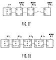
- Fig. 17 shows a first modification of the ninth embodiment of the semiconductor integrated circuit device according to the present invention.
- This first modification is of single CPU semiconductor integrated circuit device, in which a semiconductor chip 81 having a CPU and a plurality of memories 82 1 , ..., 82 n are arranged adjacent to each other in a line and further connected to each other by boding wires, respectively.
- the power consumption can be reduced, and further a large amount of data can be accessed by the CPU at high speed.
- Fig. 18 shows a second modification of the ninth embodiment of the semiconductor integrated circuit device according to the present invention.
- This second modification is of multi-CPU semiconductor integrated circuit device, in which a plurality of semiconductor chips 81 1 , .., 81 n each including a CPU and a memory 82 are arranged adjacent to each other in a line and further connected to each other by boding wires.
- the construction of the small-amplitude input/output circuits 91 and 94 is the same as that of the small-amplitude input/output circuit 87 shown in Fig. 15A.
- the small-amplitude signal transmitted from the adjacent semiconductor chip via the bonding wire 98 is detected by the small-amplitude input/output circuit 91, converted into a large-amplitude signal vibrating between the drive voltage V DD and the ground voltage GND, for instance, and then transmitted to the selector 92 a . Further, on the basis of the control signal (not shown) applied to the selector 92a, the large-amplitude signal is selectively transmitted through the selector 92a to the function block 93 or bypassed to the small-amplitude input/output circuit 94 via the bus 92c and the selector 92b.
- the large-amplitude signal transmitted to the small-amplitude input/output circuit 94 is converted into a small-amplitude signal by the small-amplitude input/output circuit 94, and then transmitted to the adjacent semiconductor chip via the pad 96 and the bonding wire 99.
- the small-amplitude signal transmitted from the adjacent semiconductor chip via the bonding wire 99 is detected and further converted into a large-amplitude signal by the small-amplitude input/output circuit 94 and then transmitted to the selector 92b. Further, on the basis of the control signal (not shown) applied to the selector 92b, the large-amplitude signal is selectively transmitted through the selector 92b to the function block 93 or bypassed to the small-amplitude input/output circuit 91 via the bus 92c and the selector 92a. The large-amplitude signal transmitted to the small-amplitude input/output circuit 91 is converted into a small-amplitude signal, and then transmitted to the adjacent semiconductor chip via the pad 95 and the bonding wire 98.
- the transmitted signals are of small-amplitude signal, it is possible to reduce the power consumption of the driver circuits of the small-amplitude input/output circuits, respectively, with the result that the semiconductor integrated circuit device can be minimized.
- Fig. 20 shows an eleventh embodiment of the semiconductor integrated circuit device according to the present invention.
- This embodiment is different from the tenth embodiment shown in Fig. 19 in that two small-amplitude input/output circuits 110 and 111 are additionally connected on both ends of the bypassing bus 92c.
- This embodiment is effective when the capacitance of the bypass 92C is large. In this construction, it is of course possible to reduce the power consumption of the semiconductor integrated circuit device.
- Fig. 21 shows a twelfth embodiment of the semiconductor integrated circuit device according to the present invention.
- four semiconductor chips 120 11 , 120 12 , 120 13 , and 120 22 are arranged in a matrix pattern and further connected to each other by bonding wires.
- each semiconductor chip is composed of the two small-amplitude input/output circuits 91 and 94, the switch circuit 92, the function block 93, and the two pads 95 and 96. Therefore, since the signals transmitted between the semiconductor chips are of small-amplitude signal, it is possible to reduce the power of the driver circuit of the small-amplitude input/output circuit and thereby to minimize the power consumption thereof.
- Fig. 22 shows a thirteenth embodiment of the semiconductor integrated circuit device according to the present invention.
- a plurality of semiconductor chips 130 11 , 130 12 , ..., 130 mn arranged in a matrix pattern (m x n units) are connected to each other by bonding wires.
- each of the four corner semiconductor chips 130 11 , 130 1n , 130 m1 and 130 mn arranged at four corners of the matrix pattern is constructed as shown in Fig. 15B.
- each of the semiconductor chips comprises three small-amplitude input/output circuits 151, 152 and 153; a switch circuit 155, a function block 156, three pads 157 1 , 157 2 and 157 3 .
- the pad 157 1 is connected to the small-amplitude input/output circuit 151; the pad 157 2 is connected to the small-amplitude input/output circuit 152; and the pad 157 3 is connected to the small-amplitude input/output circuit 153.
- the small-amplitude signals each transmitted from each adjacent semiconductor chip via each of the pads 157 i is detected by each of the small-amplitude input/output circuits 151, 152 and 153, converted into a large-amplitude signal vibrating between the drive voltage V DD and the ground voltage GND, for instance, and then transmitted to the switch circuit 155. Further, on the basis of the control signal (not shown) applied to the switch circuit 155, the large-amplitude signal is selectively transmitted through the switch circuit 155 to the function block 156 or bypassed to the other small-amplitude input/output circuit. The large-amplitude signal transmitted to the small-amplitude input/output circuit is converted into a small-amplitude signal, and then transmitted to the adjacent semiconductor chip via the corresponding pad and
- the large-amplitude signal is transmitted to the function block 156, the transmitted large-amplitude signal is processed.
- the output of the function block 156 is transmitted to the small-amplitude input/output circuit via the switch circuit, converted into a small-amplitude signal, and then transmitted to the adjacent semiconductor chip via the corresponding pad.
- the pad 147 1 is connected to the small-amplitude input/output circuit 141 and further connected to the adjacent semiconductor chip via a bonding wire; the pad 147 2 is connected to the small-amplitude input/output circuit 142 and further connected to the adjacent semiconductor chip via a bonding wire; the pad 147 3 is connected to the small-amplitude input/output circuit 143 and further connected to the adjacent semiconductor chip via a bonding wire; and the pad 147 4 is connected to the small-amplitude input/output circuit 144 and further connected to the adjacent semiconductor chip via a bonding wire.
- the small-amplitude signal transmitted from the adjacent semiconductor chip via the pads is detected and further converted into a large-amplitude signal and then transmitted to the switch circuit 145. Further, on the basis of the control signal (not shown) applied to the switch circuit 145, the large-amplitude signal is selectively transmitted through the switch circuit 145 to the function block 146 or bypassed to the other small-amplitude input/output circuit. The large-amplitude signal transmitted to the small-amplitude input/output circuit is converted into a small-amplitude signal, and then transmitted to the adjacent semiconductor chip via the corresponding pad and bonding wire.
- the transmitted large-amplitude signal is processed.
- the output of the function block 146 is transmitted to the small-amplitude input/output circuit via the switch circuit 145, converted into a small-amplitude signal, and then transmitted to the adjacent semiconductor chip via the corresponding pad.
- the signal transmitted between the chips is of small-amplitude signal, it is possible to reduce the power of the driver circuits of the small-amplitude input/output circuits, respectively, with the result that the power consumption of the semiconductor integrated circuit device can be minimized.
- the chips are connected by use of bonding wires, it is also possible to connect these chips directly by use of substrate wires.
- pads 161a, 161b, 161c and 161d are formed on a package substrate 160; and further bumps 162a, 162b, 162c and 162d are formed on these pads, respectively.
- the pad 161a and the pad 161c are connected to each other by a substrate wire 165a, and the pad 161b and the pad 161d are connected to each other by a substrate wire 165b. Further, pads 171a and 171b are formed on the surface of a semiconductor chip 171, and pads 172a and 172b are formed on the surface of another semiconductor chip 172.
- the pads 171a and 171b formed on the semiconductor chip 171 are connected to the pads 161a and 161b formed on the package substrate 160 via the bumps 162a and 162b, respectively; and the pads 172a and 172b formed on the semiconductor chip 172 are connected to the pads 161c and 161d formed on the package substrate 160 via the bumps 162c and 162d, respectively.
- Fig. 25 shows a fourteenth embodiment of the semiconductor integrated circuit device according to the present invention, in which a plurality of semiconductor chips 180 1 , .., 180 n arranged in a line on the same plane are connected to each other through two buses 186 and 187.
- the semiconductor chip 180 1 is provided with a small-amplitude output circuit composed of the bias circuit 1 A and the driver circuit 5 A , and the small-amplitude input circuit composed of the voltage divider circuit 9 A and the receiver circuit 10 A , in the same way as with the case of the semiconductor chip A of the seventh embodiment shown in Fig. 12.
- the output terminal of the voltage divider circuit 9 A is connected to the pad 182 1
- the output terminal of the driver circuit 5 A is connected to the pad 183 1 .
- the other semiconductor chips 180 i are provided with a small-amplitude output circuit composed of the driver circuit 5 B , and the small-amplitude input circuit composed of the voltage divider circuit 9 B and the receiver circuit 10 B , respectively, in the same way as with the case of the semiconductor chip B of the seventh embodiment shown in Fig. 12.
- the output terminal of the voltage divider circuit 9 B is connected to the pad 182 i
- the output terminal of the driver circuit 5 B is connected to the pad 183 i .
- the signals transferred between the semiconductor chips are of small-amplitude signal, in the same way as with the case of the seventh embodiment, it is possible to reduce the power of the driver circuits, so that the power consumption thereof can be minimized.
- the semiconductor chips are connected through the two buses, it is possible to transmit signals at a high speed by a small power. Further, signals transmitted from one chip can be received by the other chips at the same time.
- Fig. 26 shows a fifteenth embodiment of the semiconductor integrated circuit device according to the present invention, in which a plurality of the semiconductor chips 180 1 , .., 180 n arranged in the fourteenth embodiment shown in Fig. 25 are laminated one upon another. This structure is referred to as a multi-chip semiconductor device.
- the buses 186 and 187 are constructed by junction wires for connecting the respective chips.
- the bias circuit on the other semiconductor chip 180 i (i ⁇ 1) on which no bias circuit is provided.
- the pads 182 1 , .., 182 n and the bus 186 can be eliminated.
- one of the two output ends of the driver circuit 5 A is connected to the pad 182 i , and the other of the two output ends thereof is connected to the pad 183 i .
- the bias circuit is constructed by the N-channel transistors, it is of course possible to construct the bias circuit by use of P-channel transistors. In this case, the drive voltage V DD and the ground voltage GND must be reversed with respect to each other.
- the signals flowing through the transfer path are of small-amplitude signal
- the power of the driver circuits for driving the transfer path can be reduced, with the result that the power consumption of the semiconductor integrated circuit can be minimized.
Landscapes
- Engineering & Computer Science (AREA)
- Computer Hardware Design (AREA)
- Physics & Mathematics (AREA)
- Computing Systems (AREA)
- General Engineering & Computer Science (AREA)
- Mathematical Physics (AREA)
- Logic Circuits (AREA)
- Dc Digital Transmission (AREA)
- Memory System (AREA)
- Semiconductor Integrated Circuits (AREA)
- Amplifiers (AREA)
- Dram (AREA)
Abstract
Description
- The present invention relates to a semiconductor integrated circuit device having driver circuits each for driving a bus, a clock line or an input/output line of a semiconductor chip.
- The power consumption of a CMOS circuit can be given by the following formula:

- In the ordinary circuit, conventionally since the amplitude of the signal changes between the supply voltage and the ground voltage, the above formula (1) can be expressed as

- In the ordinary CMOS circuit, however, since there exist relatively large parasitic capacitances in the bus and clock line, or the input/output line of the semiconductor chip, the driver circuits for driving these lines consume a relatively large power, respectively. Recently, therefore, a lower power consumption has been required more and more for the semiconductor integrated circuit device, so that this problem has become an important problem to be solved.
- By the way, as understood on the basis of the above formula (1), one of the methods of reducing the power consumption is to reduce the signal amplitude. However, this method is not easy. The reasons are as follows: first, it is difficult to realize the driver circuit for outputting a small amplitude signal under a low power consumption. Or else, it is difficult to realize a receiver circuit for receiving the small-amplitude signal and returning the received small-amplitude signal to the ordinary amplitude signal under a low power consumption.
- In addition, in the case of the small-amplitude signal, since the margin against noise is inevitably reduced, it is difficult to prevent erroneous signals from being transmitted. In particular, in the case of the input/output line of the chip, since the signal is susceptible to an influence of signal reflection, there exists a problem of cross talk with the ordinary signals.
- Further, there exists a problem of the threshold fluctuations of the receiver circuit due to the change of temperature and the dispersion of device characteristics.
- For the reasons as described above, the small-amplitude signals have been so far used for only a part of the circuits whose characteristics are well known (e.g., as with the case of bit line signals of a memory device). In the ordinary semiconductor circuit device, on the other hand, the signals having an amplitude changing between the supply voltage and the ground voltage have been so far used. As a result, there exists a problem in that the power consumption cannot be reduced in the semiconductor integrated circuit device having the driver circuits.
- With these problems in mind, therefore, it is the object of the present invention to provide a semiconductor integrated circuit device having driver circuits of the smallest possible power consumption.
- To achieve the above-mentioned object, a first aspect of the present invention provides a semiconductor integrated circuit device, comprising: a bias circuit for generating a predetermined voltage fixed between a first supply voltage and a second supply voltage; a driver circuit for receiving an inversion input signal and a non-inversion input signal each vibrating between the first and second supply voltages, for converting the received input signals into a signal vibrating between an output voltage of said bias circuit and the first supply voltage, and for driving a transfer path by the converted signal; a voltage divider circuit for dividing an output voltage of said bias circuit; and a receiver circuit for detecting the signal for driving the transfer path by use of an output of said voltage divider circuit as a reference voltage, and for converting the detected signal into a signal vibrating between the first supply voltage and the second supply voltage.
- Further, a second aspect of the present invention provides a semiconductor integrated circuit device, comprising: a bias circuit for generating a predetermined voltage fixed between a first supply voltage and a second supply voltage; a driver circuit for receiving an inversion input signal and a non-inversion input signal each vibrating between the first and second supply voltages, for converting the received input signals into a signal vibrating between an output voltage of said bias circuit and the first supply voltage on the basis of an enable signal, and for driving a transfer path by the converted signal or for setting an output thereof to a high impedance; a voltage divider circuit for dividing an output voltage of said bias circuit; and a receiver circuit for detecting the signal for driving the transfer path by use of an output of said voltage divider circuit as a reference voltage, and for converting the detected signal into a signal vibrating between the first supply voltage and the second supply voltage.
- Further, a third aspect of the present invention provides a semiconductor integrated circuit device, comprising: a bias circuit for generating a predetermined voltage fixed between a first supply voltage and a second supply voltage; a driver circuit for receiving an inversion input signal and a non-inversion input signal each vibrating between the first and second supply voltages, for converting the received input signals into two differential signals each vibrating between an output voltage of said bias circuit and the first supply voltage, and for driving two transfer paths by the two differential signals, respectively; and a receiver circuit for detecting the differential signals for driving the transfer paths, and for converting the detected differential signals into a signal vibrating between the first supply voltage and the second supply voltage.
- Further, a fourth aspect of the present invention provides a semiconductor integrated circuit device, comprising: a bias circuit for generating a predetermined voltage fixed between a first supply voltage and a second supply voltage; a driver circuit for receiving an inversion input signal and a non-inversion input signal each vibrating between the first and second supply voltages, for converting the received input signals into two differential signals each vibrating between an output voltage of said bias circuit and the first supply voltage on the basis of an enable signal, and for driving two transfer paths by the two differential signals or for setting two outputs thereof to a high impedance, respectively; and a receiver circuit for detecting the differential signals for driving the transfer paths, and for converting the detected differential signals into a signal vibrating between the first supply voltage and the second supply voltage.
- Further, a fifth aspect of the present invention provides a semiconductor integrated circuit device, comprising: a first semiconductor chip including: a bias circuit for generating a predetermined voltage fixed between a first supply voltage and a second supply voltage; a first driver circuit for receiving a first inversion input signal and a first non-inversion input signal each vibrating between the first and second supply voltages, for converting the received input signals into a signal vibrating between an output voltage of said bias circuit and the first supply voltage on the basis of a first enable signal, and for outputting the converted signal or for setting an output thereof to a high impedance; a first voltage divider circuit for dividing an output voltage of said bias circuit; and a first receiver circuit; and a second semiconductor chip including: a second voltage divider circuit having an input end connected to an input end of said first voltage divider circuit via a wire, for dividing an output voltage of said bias circuit; a second driver circuit having an output end connected to an output end of said first driver circuit via a transfer wire, for receiving a second inversion input signal and a second non-inversion input signal each vibrating between the first and second supply voltages, for converting the received input signals into a signal vibrating between an output voltage of said bias circuit and the first supply voltage on the basis of a second enable signal, and for outputting the converted signal or for setting an output thereof to a high impedance; and a second receiver circuit; and wherein: said first receiver circuit is activated, when the output of said first driver circuit is at the high impedance, to detect a signal transferred from said second driver circuit via the transfer wire and further to convert the detected signal into a signal vibrating between the first supply voltage and the second supply voltage; and said second receiver circuit is activated, when the output of said second driver circuit is at the high impedance, to detect a signal transferred from said first driver circuit via the transfer wire and further to convert the detected signal into a signal vibrating between the first supply voltage and the second supply voltage.
- Further, a sixth aspect of the present invention provides a semiconductor integrated circuit device, comprising: a first semiconductor chip including: a first bias circuit for generating a predetermined fixed voltage between a first supply voltage and a second supply voltage; a first driver circuit for receiving a first inversion input signal and a first non-inversion input signal each vibrating between the first and second supply voltages, for converting the received input signals into two differential signals each vibrating between an output voltage of said first bias circuit and the first supply voltage on the basis of a first enable signal, and for outputting the converted differential signals or setting two outputs thereof to a high impedance, respectively; and a first receiver circuit; and a second semiconductor chip including: a second bias circuit for generating another predetermined voltage fixed between a third supply voltage and a fourth supply voltage; a second driver circuit for receiving a second inversion input signal and a second non-inversion input signal each vibrating between the third and fourth supply voltages, for converting the received input signals into two differential signals each vibrating between an output voltage of said second bias circuit and the third supply voltage on the basis of a second enable signal, and for outputting the converted differential signals or setting two outputs thereof to a high impedance, respectively; and a second receiver circuit; and wherein: two output ends of each of said first and second driver circuits are connected to each other by a transfer wire, respectively; said first receiver circuit is activated, when the output of said first driver circuit is at the high impedance, to detect the two differential signals transferred from said second driver circuit via the transfer wires and further to convert the detected difference signals into a signal vibrating between the first supply voltage and the second supply voltage; and said second receiver circuit is activated, when the output of said second driver circuit is at the high impedance, to detect the two differential signals transferred from said first driver circuit via the transfer wire and further to convert the detected differential signals into a signal vibrating between the third supply voltage and the fourth supply voltage.
- Further, a seventh aspect of the present invention provides a semiconductor integrated circuit device, which comprises: a plurality of semiconductor chips arranged in a matrix pattern, each semiconductor chip including: input/output ends connected to input/output ends of another adjacent semiconductor chip by transfer wires of bonding wires or substrate wires, respectively, for transferring data; and a small-amplitude input/output circuit arranged in each of the input/output ends of a part or all of said semiconductor chips, for receiving a non-inversion signal and an inversion signal each vibrating between a first supply voltage and a second supply voltage according to each semiconductor chip including the small-amplitude input/output circuit, for converting the received signals into a small-amplitude signal vibrating between a predetermined voltage fixed between the first and second supply voltages and the first supply voltage, for outputting the converted signal to the input/output end of another adjacent semiconductor chip via the transfer wire, and for converting the small-amplitude signal transferred via the transfer wire into a signal vibrating between the first supply voltage and the second supply voltage.
- Further, an eighth aspect of the present invention provides a semiconductor integrated circuit device, comprising: first to n-th semiconductor chips arranged in a line, said first semiconductor chip including: first functioning means having predetermined processing functions; a first input/output end for transferring data; and a first small-amplitude input/output circuit for converting an output of said first functioning means into a small-amplitude signal having an amplitude smaller than that of the output signal of said first functioning means, for transferring the converted small-amplitude signal to the adjacent second semiconductor chip via said first input/output end, for converting a small-amplitude signal transferred from the second semiconductor chip via said first input/output end into a large-amplitude signal having an amplitude larger than that of the transferred small-amplitude signal, and for transferring the converted large-amplitude signal to said first functioning means; said i-th (i=2, .., n-1) semiconductor chip including: i-th functioning means having predetermined processing functions; 2(i-1)-th and (2i-1)-th input/output ends each for transferring data; 2(i-1)-th and (2i-1)-th small-amplitude input/output circuits; and an (i-1)-th switch circuit; said (i-1)-th switch circuit transferring an output of said i-th functioning means to the 2(i-1)-th or the (2i-1)-th small-amplitude input/output circuit on the basis of a control signal, and selectively outputting an output of one of the 2(i-1)-th and (2i-1)-th small-amplitude input/output circuits to the i-th functioning means or bypasses the same output to the other of the 2(i-1)-th and the (2i-1)-th small-amplitude input/output circuits on the basis of the same control signal; the 2(i-1)-th small-amplitude input/output circuit converting an output of said (i-1)-th switch circuit into a small-amplitude signal having an amplitude smaller than that of the output signal, transferring the converted small-amplitude signal to the (i-1)-th semiconductor chip via said 2(i-1)-th input/output end, converting a small-amplitude signal transferred from the (i-1)-th semiconductor chip via the 2(i-1)-th input/output end into a large-amplitude signal having an amplitude larger than that of the transferred signal, and transferring the converted large-amplitude signal to said (i-1)-th switch circuit; and the (2i-1)-th small-amplitude input/output circuit converting an output of said (i-1)-th switch circuit into a small-amplitude signal having an amplitude smaller than that of the output signal, transferring the converted small-amplitude signal to the (i+1)-th semiconductor chip via said (2i-1)-th input/output end, converting a small-amplitude signal transferred from the (i+1)-th semiconductor chip via the (2i-1)-th input/output end into a large-amplitude signal having an amplitude larger than that of the transferred signal, and transferring the converted large-amplitude signal to said (i-1)-th switch circuit; said n-th semiconductor chip including: n-th functioning means having predetermined processing functions; 2(n-1)-th input/output end for transferring data; and 2(n-1)-th small-amplitude input/output circuit for converting an output of said n-th functioning means into a small-amplitude signal having an amplitude smaller than that of the output, for transferring the converted signal to the adjacent (n-1)-th semiconductor chip via the 2(n-1)-th input/output end, for converting the small-amplitude signal transferred from the (n-1)-th semiconductor chip via the 2(n-1)-th input/output end into a large-amplitude signal having an amplitude larger than that of the small-amplitude signal, and for transferring the converted signal to the n-th functioning means; and the (2i-1)-th input/output end of said i-th (i=1, .., n-1) semiconductor chip being connected to the 2i-th input/output end of said (i+1)-th semiconductor chip by a transfer wire of a bonding wire or a substrate wire.
- Further, a ninth aspect of the present invention provides a semiconductor integrated circuit device, comprising: first to n-th semiconductor chips arranged in a line, said first semiconductor chip including: first functioning means having predetermined processing functions; a first input/output end for transferring data; and a first small-amplitude input/output circuit for converting an output of said first functioning means into a small-amplitude signal having an amplitude smaller than that of the output signal, for transferring the converted small-amplitude signal to the adjacent second semiconductor chip via said first input/output end, for converting a small-amplitude signal transferred from the second semiconductor chip via the first input/output end into a large-amplitude signal having an amplitude larger than that of the transferred small-amplitude signal, and for transferring the converted large-amplitude signal to said first functioning means; said i-th (i=2, .., n-1) semiconductor chip including: i-th functioning means having predetermined processing functions; 2(i-1)-th and (2i-1)-th input/output ends each for transferring data; 2(i-1)-th and (2i-1)-th small-amplitude input/output circuits; and 2(i-1)-th and (2i-1)-th selector circuits; and said 2(i-1)-th small-amplitude input/output circuit converting a small-amplitude signal transferred from the adjacent (i-1)-th semiconductor chip via the 2(i-1)-th input/output end into a large-amplitude signal having an amplitude larger than that of the small-amplitude signal, transferring the converted signal to the 2(i-1)-th selector circuit, converting the signal transferred from the 2(i-1)-th selector circuit into a signal having an amplitude smaller than that of the selector signal, and transferring the converted signal to the (i-1)-th semiconductor chip via the 2(i-1)-th input/output end; said (2i-1)-th small-amplitude input/output circuit converting a small-amplitude signal transferred from the adjacent (i+1)-th semiconductor chip via the (2i-1)-th input/output end to a large-amplitude signal having an amplitude larger than that of the small-amplitude signal, transferring the converted signal to the (2i-1)-th selector circuit, converting the signal transferred from the (2i-1)-th selector circuit into a signal having an amplitude smaller than that of the selector signal, and transferring the converted signal to the (i+1)-th semiconductor chip via the (2i-1)-th input/output end; the 2(i-1)-th selector circuit transferring an output of the i-th functioning means and a signal of the (2i-1)-th selector circuit to the 2(i-1)-th small-amplitude input/output circuit, and selectively transferring a signal from the 2(i-1)-th small-amplitude input/output circuit to the i-th functioning means or the (2i-1)-th selector circuit on the basis of a control signal; the (2i-1)-th selector circuit transferring an output of the i-th functioning means and a signal of the 2(i-1)-th selector circuit to the (2i-1)-th small-amplitude input/output circuit, and selectively transferring a signal from the (2i-1)-th small-amplitude input/output circuit to the i-th functioning means or the 2(i-1)-th selector circuit on the basis of the control signal; said n-th semiconductor chip including: n-th functioning means having predetermined processing functions; 2(n-1)-th input/output end for transferring data; and 2(n-1)-th small-amplitude input/output circuit for converting an output of said n-th functioning means into a small-amplitude signal having an amplitude smaller than that of the output, for transferring the converted signal to the adjacent (n-1)-th semiconductor chip vial the 2(n-1)-th input/output end, for converting the small-amplitude signal transferred from the (n-1)-th semiconductor chip via the 2(n-1)-th input/output end into a large-amplitude signal having an amplitude larger than that of the small-amplitude signal, and for transferring the converted signal to the n-th functioning means.
-
- Fig. 1 is a block diagram showing a first embodiment of the semiconductor integrated circuit device according to the present invention;
- Fig. 2 is a block diagram showing a second embodiment of the semiconductor integrated circuit device according to the present invention;
- Fig. 3 is a circuit diagram showing a practical example of a voltage divider circuit of the first and second embodiments of the semiconductor integrated circuit device according to the present invention;
- Fig. 4 is a block diagram showing a third embodiment of the semiconductor integrated circuit device according to the present invention;
- Fig. 5 is a block diagram showing a fourth embodiment of the semiconductor integrated circuit device according to the present invention;
- Fig. 6 is a circuit diagram showing a circuit for generating two input signals applied to the driver circuit related to the semiconductor integrated circuit device according to the present invention;
- Fig. 7 is a circuit diagram showing a practical example of a sense amplifier circuit of a receiver circuit related to the semiconductor integrated circuit device according to the present invention;
- Fig. 8 is a circuit diagram showing another practical example of the sense amplifier circuit of the receiver circuit related to the semiconductor integrated circuit device according to the present invention;
- Fig. 9 is a block diagram showing a fifth embodiment of the semiconductor integrated circuit device according to the present invention;
- Fig. 10 is a circuit diagram showing a practical example of a bus terminator circuit used for the fifth embodiment of the semiconductor integrated circuit device according to the present invention;
- Fig. 11 is a block diagram showing a sixth embodiment of the semiconductor integrated circuit device according to the present invention;
- Fig. 12 is a block diagram showing a seventh embodiment of the semiconductor integrated circuit device according to the present invention;
- Fig. 13 is a block diagram showing an eighth embodiment of the semiconductor integrated circuit device according to the present invention;
- Fig. 14 is a block diagram showing a ninth embodiment of the semiconductor integrated circuit device according to the present invention;
- Figs. 15A and 15B are block diagrams each showing a switch circuit related to the ninth embodiment of the semiconductor integrated circuit device according to the present invention;
- Fig. 16A is a block diagram showing a switch circuit related to a semiconductor chip shown in Fig. 15B;
- Fig. 16B is a circuit diagram showing a structure of each switch element shown in Fig. 16A;
- Fig. 16C is a table for listing the connection relationship of the respective nodes on the basis of the control signals applied to the respective switch elements shown in Fig. 16A;
- Fig. 17 is a block diagram showing a first modification of the ninth embodiment;
- Fig. 18 is a block diagram showing a second modification of the ninth embodiment;
- Fig. 19 is a block diagram showing a tenth embodiment of the semiconductor integrated circuit device according to the present invention;
- Fig. 20 is a block diagram showing an eleventh embodiment of the semiconductor integrated circuit device according to the present invention;
- Fig. 21 is a block diagram showing a twelfth embodiment of the semiconductor integrated circuit device according to the present invention;
- Fig. 22 is a block diagram showing a thirteenth embodiment of the semiconductor integrated circuit device according to the present invention;
- Figs. 23A and 23B are block diagrams each showing a semiconductor chip related to the thirteenth embodiment according to present invention;
- Fig. 24 is a perspective view showing substrate wires;
- Fig. 25 is a block diagram showing fourteenth embodiment of the semiconductor integrated circuit device according to the present invention; and
- Fig. 26 is a block diagram showing a fifteenth embodiment of the semiconductor integrated circuit device according to the present invention.
- Some embodiments of the semiconductor integrated circuit device according to the present invention will be described hereinbelow with reference to the attached drawings.
- Fig. 1 shows a first embodiment thereof, which comprises a small-amplitude output circuit having a
bias circuit 1 and adriver circuit 5, avoltage divider circuit 9, and areceiver circuit 10 having a sense amplifier circuit. - The
bias circuit 1 generates a predetermined voltage, which comprises acurrent source 2, a series circuit constructed by connecting an n-units of N-channel MOS transistors M1, M2, ..., Mn of the same size in series, an N-channel MOS transistor 3, and acapacitor 4. Each gate terminal of each transistor Mi (i=1 .., n) is connected to each drain terminal thereof; the drain terminal of the transistor Mn is connected to an output terminal of thecurrent source 2; and the source terminal of the transistor M1 is grounded. On the other hand, the drain terminal of thetransistor 3 is connected to a drive voltage supply VDD; the gate terminal thereof is connected to the drain terminal of the transistor Mn; and the source terminal thereof is grounded via thecapacitor 4. - Therefore, when each threshold voltage of each transistor Mi (i=1, .., n) is denoted by Vth, the voltage at the drain terminal of the transistor Mn is n·Vth.
- Further, since the threshold voltage of the
transistor 3 can be set to Vth, the voltage at the source terminal of thetransistor 3; that is, the voltage at the output terminal NV of thebias circuit 1 can be set to a constant voltage of
capacitor 4 is connected to stabilize the voltage at the output terminal of thebias circuit 1, it is possible to improve the transient response of the output of thedriver circuit 1. However, thiscapacitor 4 can be omitted. - The
driver circuit 5 receives a non-inversion input signal and an inversion input signal both vibrating between the drive voltage VDD and the ground voltage GND, converts the received input signals into a small-amplitude signal vibrating between the output voltage of thebias circuit 1 and the ground voltage GND, and drives atransfer path 100 such as a bus, a clock line, etc. on the basis of the converted small-amplitude signal. - The
driver circuit 5 comprises two series-connected N-channel MOS transistors transistor 61 is connected to the output terminal NV of the bias circuit; the source thereof is connected to the drain of thetransistor 62; and the gate thereof receives a non-inversion input signal. Further, the source of thetransistor 62 is grounded; and the gate thereof receives an inversion input signal. Further, an output signal of thedriver circuit 5 is outputted from a junction point between the twotransistors transfer path 100. - The
voltage divider circuit 9 divides the output voltage of thebias circuit 1, which can be constructed by a plurality of series-connected resistors (e.g., R1 and R2 as shown in Fig. 3). - The
receiver circuit 10 detects the small-amplitude signal transmitted through thetransfer path 100 by a sense amplifier circuit by use of the output voltage of thevoltage divider circuit 9 as a reference voltage, and converts the detected small-amplitude signal into a signal vibrating between the drive voltage VDD and the ground voltage GND. - As described above, in the first embodiment of the semiconductor integrated circuit device according to the present invention, it is possible to convert the output of the
driver circuit 5 for driving thetransfer path 100 such as the bus, the clock line, etc. into the small-amplitude signal. In general, the power consumption of the driver circuit is proportional to the amplitude of the output signal. Therefore, the power consumption of this first embodiment can be reduced in comparison with that of the prior art semiconductor integrated circuit device. - Further, in the above-mentioned embodiment, although a plurality of N-channel transistors are of the same size in the series-connected circuit of the
bias circuit 1, the series-connected circuit thereof can be composed of a plurality of N-channel transistors of different sizes. - Fig. 2 shows a second embodiment of the semiconductor integrated circuit device according to the present invention, which is different from the first embodiment shown in Fig. 1 in that two NOR
gates driver circuit 5. - The NOR
gate 71 executes NOR operation on the basis of the non-inversion input signal and an enable signal, and transmits the operation result to the gate of thetransistor 61. On the other hand, the NORgate 72 executes NOR operation on the basis of the inversion input signal and the same enable signal, and transmits the operation result to the gate of thetransistor 62. - Therefore, in this second embodiment, when the enable signal is at an L-level, the operation is the same as with the case of that of the first embodiment. On the other hand, when the enable signal is at an H-level, the output of the
driver circuit 5 is set to a high impedance. - In this second embodiment, it is of course possible to obtain the same effect as with the case of the first embodiment.
- Fig. 4 shows a third embodiment of the semiconductor integrated circuit device according to the present invention, which is different from the first embodiment shown in Fig. 1 in that the
voltage divider circuit 9 is omitted and further two series-connected N-channel MOS transistors driver circuit 5. - The drain of the
transistor 63 is connected to the output terminal of thebias circuit 1; the source thereof is connected to the drain of thetransistor 64; and the gate thereof receives the inversion input signal. On the other hand, the source of thetransistor 64 is grounded; and the gate thereof receives the non-inversion input signal. - Further, the non-inversion small-amplitude signal can be transmitted from the junction point between the two
transistors receiver circuit 10 via thetransfer path 1001. On the other hand, the inversion small-amplitude signal can be transmitted from the junction point between the twotransistors receiver circuit 10 via thetransfer path 1002. - Therefore, in this third embodiment, the
driver circuit 5 can drive the twotransfer paths 
receiver circuit 10 detects the differential signal transmitted through the twotransfer paths - In this third embodiment, it is of course possible to obtain the same effect as with the case of the first embodiment and further to minimize the power consumption.
- Further, in this third embodiment, although two transfer paths are needed, since the reference voltage applied to the sense amplifier circuit is not needed, it is possible to obtain a wide operation margin against the same-phase noise.
- Fig. 5 shows a fourth embodiment of the semiconductor integrated circuit device according to the present invention, which is different from the third embodiment shown in Fig. 4 in that two NOR
gates driver circuit 5. - The NOR
gate 71 executes NOR operation on the basis of the non-inversion input signal and an enable signal, and transmits the operation result to the gates of the twotransistors gate 72 executes NOR operation on the basis of the inversion input signal and the same enable signal, and transmits the operation result to the gates of the twotransistor - Therefore, in this fourth embodiment, when the enable signal is at the L-level, the operation is the same as with the case of that of the third embodiment. On the other hand, when the enable signal is at the H-level, the output of the
driver circuit 5 is set to a high impedance. - In this fourth embodiment, it is of course possible to obtain the same effect as with the case of the first embodiment and further to minimize the power consumption.
- The non-inversion input signal and the inversion input signal used in the first to fourth embodiments can be generated by a circuit as shown in Fig. 6. The circuit shown in Fig. 6 is composed of two
inversion gates - Further, the sense amplifier circuit used for the first to fourth embodiments can be constructed by a circuit as shown in Fig. 7. The circuit shown in Fig. 7 is composed of a
current source 25, two P-channel MOS transistors 261 and 262 for receiving a differential input signal, and two N-channel MOS transistors 271 and 272. Further, in the case of the first and second embodiments, the output of thevoltage divider circuit 9 is inputted to the gate of the transistor 262. - In the same way, the sense amplifier circuit can be constructed as shown in Fig. 8. The sense amplifier shown in Fig. 8 is composed of a P-
channel MOS transistor 31 for receiving a control signal at the gate thereof; two P-channel MOS transistors 321 and 322 for receiving a differential input signal at the gate thereof; two common-gate and series-connected P-channel MOS transistor 331 and N-channel MOS transistor 341; and two common-gate and series-connected P-channel MOS transistor 332 and N-channel MOS transistor 342. - Fig. 9 shows a fifth embodiment of the semiconductor integrated circuit device according to the present invention, which is different from the second embodiment shown in Fig. 2 in that a
bus terminator circuit 40 is additionally connected between the output terminal of thebias circuit 1 and thetransfer path 100. Thisbus terminator circuit 40 can maintain the voltage at the transfer path 100 (e.g., bus) when the output of thedriver circuit 5 is set to a high impedance. - As shown in Fig. 10, this
bus terminator circuit 40 can be constructed by two P-channel MOS transistors 411 and 412, and two N-channel MOS transistors 421 and 422. The source of the transistor 41i (i=1 and 2) is connected to the output terminal NV of thebias circuit 1; the gate thereof is connected to the gate of the transistor 42i (i=1) and 2); and the drain thereof is connected to the drain of the transistor 42i. Further, the source of the transistor 42i (i= 1 and 2) is grounded. Further, the drains of the two transistors 411 and 421 are connected to the gates of the two transistors 412 and 422. On the other hand, the drains of the two transistors 412 and 422 are connected to the gates of the two transistors 411 and 421. Further, the drains of the two transistors 411 and 421 are connected to thetransfer path 100. - In this third embodiment, it is of course possible to obtain the same effect as with the case of the first embodiment and further to minimize the power consumption. Further, it is possible to maintain the voltage at the transfer path 100 (e.g., bus) at a predetermined voltage, when the output of the
driver circuit 5 is set to a high impedance. - Fig. 11 shows a sixth embodiment of the semiconductor integrated circuit device according to the present invention, which is different from the fourth embodiment shown in Fig. 5 in that a
bus terminator circuit 40 is additionally connected between the output terminal of thebias circuit 1 and the twotransfer paths bus terminator circuit 40 can maintain the voltages at the twotransfer paths driver circuit 5 are set to a high impedance, respectively. - This
bus terminator circuit 40 can be constructed as shown in Fig. 10. In this case, thetransfer path 1001 is connected to the drains of the two transistors 411 and 421, and thetransfer path 1002 is connected to the drains of the two transistors 412 and 422, respectively. - In this sixth embodiment, it is possible to minimize the power consumption, as with the case of the fourth embodiment. Further, it is possible to maintain the voltages at the two
transfer paths driver circuit 5 are set to a high impedance, respectively. - Further, in the first to sixth embodiments, the
driver circuit 5 and thereceiver circuit 10 can be driven by the same voltage supply or two different voltage supplies. - Fig. 12 shows a seventh embodiment of the semiconductor integrated circuit device according to the present invention. In this embodiment, the semiconductor integrated circuit device comprises two semiconductor chips. Therefore, a
bias circuit 1A, adriver circuit 5A, avoltage divider circuit 9A and areceiver circuit 10A are provided for the semiconductor chip A. Further, acapacitor 4B, adriver circuit 5B, avoltage divider circuit 9B and areceiver circuit 10B are provided for the semiconductor chip B. - Here, the
bias circuit 1A, thedriver circuits voltage divider circuits bias circuit 1, thedriver circuit 5 and thevoltage divider circuit 9 of the second embodiment, respectively. - In Fig. 12, the output terminal NV of the
bias circuit 1A is connected to the input terminal of thevoltage divider circuit 9A and further to a pad 51A formed on the semiconductor chip A. Further, the input terminal of thevoltage divider circuit 9B and one end of thecapacitor 4B are connected to a pad 51B formed on the chip B. These two chips A and B are arranged at the nearest possible distance and two pads 51A and 51B are connected to each other by aboding wire 61. Therefore, the output voltage of thebias circuit 1A is applied to thevoltage divider circuit 9B and thecapacitor 4B of the chip B via the pad 51A, thebonding wire 61 and the pad 51B. Further, thecapacitor 4B is connected to maintain the voltage at the input terminal of thevoltage divider circuit 9B stably. However, thiscapacitor 4B can be omitted. - Further, the output terminal of the
driver circuit 5A is connected to a pad 52A formed on the chip A, and the output terminal of thedriver circuit 5B is connected to a pad 52B formed on the chip B. These two pads 52A and 52B are connected to each other via abonding wire 62. Further, the drain of thetransistor 61 of thedriver circuit 5B is connected to the pad 51B. - On the other hand, the
receiver circuit 10A detects the output of thedriver circuit 5B transmitted through thebonding wire 62 by the sense amplifier circuit by use of the output voltage of thevoltage divider circuit 9A as a reference voltage, and converts the detected output into a signal vibrating between the drive voltage VDD and the ground voltage GND. Further, thereceiver circuit 10B detects the output of thedriver circuit 5A transmitted through thebonding wire 62 by the sense amplifier circuit by use of the output voltage of thevoltage divider circuit 9B as a reference voltage, and converts the detected output into a signal vibrating between the drive voltage VDD and the ground voltage GND. - Accordingly, in this seventh embodiment, when the
driver circuit 5A is being activated, although thereceiver circuit 10B is also activated, thedriver circuit 5B and thereceiver circuit 10A are both deactivated. Further, when thedriver circuit 5B is being activated, although thereceiver circuit 10A is also activated, thedriver circuit 5A and thereceiver circuit 10B are both deactivated. As described above, in this embodiment, since the signal transmitted between the two chips A and B is of small-amplitude signal, it is possible to reduce the power of the driver circuits, respectively, with the result that the power consumption of the semiconductor integrated circuit device can be minimized. - Further, in this embodiment, the small-amplitude output circuit composed of the
bias circuit 1A and thedriver circuit 5A, and the small amplitude input circuit composed of thevoltage divider circuit 9A and thereceiver circuit 10A are provided on the chip A. Further, the small-amplitude output circuit composed of thedriver circuit 5B, and the small amplitude input circuit composed of thevoltage divider circuit 9B and thereceiver circuit 10B are provided on the chip B. - Further, in this embodiment, since the two chips are arranged at the nearest possible distance and further since the two chips are connected to each other by the bonding wires, the output capacitance can be reduced. Further, even if the impedance matching is not considered between the inter-chip bonding wire and the driver circuit, a large signal reflection will not be developed.
- Further, in this embodiment, the bias circuit can be formed on the chip B. In this case, the
bonding wire 61 can be eliminated. Further, in this case, the same voltage supply can be used for both the chips A and B, or else two different voltage supplies can be used for both the chips A and B, respectively. Further, in the above-mentioned embodiment, although the two chips are connected to each other by use of the boding wires, it is also possible to connect the two chips directly by use of wires formed on the substrate. - Fig. 13 shows an eighth embodiment of the semiconductor integrated circuit device according to the present invention. In this embodiment, the small-amplitude input circuit and the small-amplitude output circuit are provided for each of the two semiconductor chips A and B arranged at the nearest possible distance. The small-amplitude output circuit of the chip A is composed of the
bias circuit 1A and thedriver circuit 5A, and the small-amplitude input circuit of the chip A is composed of thereceiver circuit 10A. Further, the small-amplitude output circuit of the chip B is composed of thebias circuit 1B and thedriver circuit 5B, and the small-amplitude input circuit of the chip B is composed of thereceiver circuit 10B. - The circuit constructions of the
bias circuits driver circuits bias circuit 1 and thedriver circuit 5 of the fourth embodiment shown in Fig. 5. Further, the two outputs of thedriver circuit 5A are connected to two pads 53A and 54A formed on the chip A, respectively. Further, the two outputs of thedriver circuit 5B are connected to two pads 53B and 54B formed on the chip B, respectively. The pad 53A formed on the chip A and the pad 53B formed on the chip B are connected to each other by abonding wire 63, and the pad 54A formed on the chip A and the pad 54B formed on the chip B are connected to each other by abonding wire 64. - On the other hand, the
receiver circuit 10A detects the small-amplitude differential output of thedriver circuit 5B transmitted through the twobonding wires receiver circuit 10B detects the small-amplitude differential output of thedriver circuit 5A transmitted through the twobonding wires - Accordingly, in this embodiment, when the
driver circuit 5A is being activated, although thereceiver circuit 10B is also activated, thedriver circuit 5B and thereceiver circuit 10A are both deactivated. Further, when thedriver circuit 5B is being activated, although thereceiver circuit 10A is also activated, thedriver circuit 5A and thereceiver circuit 10B are both deactivated. - As described above, in this embodiment, since the signal transmitted between the two chips A and B is of small-amplitude signal, it is possible to reduce the power of the driver circuits, respectively, with the result that the power consumption of the semiconductor integrated circuit device can be minimized.
- Further, in this embodiment, since the two chips are arranged at the nearest possible distance and further since the two chips are connected to each other by the bonding wires, the output capacitance can be reduced. Further, even if the impedance matching is not considered between the interchip bonding wire and the driver circuit, a large signal reflection will not be developed.
- Further, in this embodiment, although the same voltage supply is used for both the chips A and B, it is also possible to use two different voltage supplies for both the chips A and B, respectively.
- Further, in the seventh and eighth embodiments, the two chips A and B connected to each other by use of bonding wires can be mounted on the same lead frame base, and then sealed by use of a resin.
- A ninth embodiment of the semiconductor integrated circuit device according to the present invention will be described hereinbelow with reference to Fig. 14 and Figs. 15A and 15B.
- Fig. 14 is an entire circuit construction of this embodiment, in which a plurality of
semiconductor chips 721, ..., 72n arranged in a line are connected to each other by use ofbonding wires 77. Thesemiconductor chip 721 has apad 74; the semiconductor chip 72i (i=2, .., n-1) haspads semiconductor chip 72n has apad 75, respectively. Further, two adjacent semiconductor chips 72i (i=2, .., n-1) and thesemiconductor chip 72i+1 are arranged at the nearest possible distance, and further thepad 74 of thesemiconductor chip 72i and thepad 75 of thesemiconductor chip 72i+1 are connected to each other by the bodingwire 77. - Each of the semiconductor chips 721 and 72n arranged on both the ends is constructed as a chip 85 shown in Fig. 15A. That is, the end chip 85 is provided with a
function block 86, a small-amplitude input/output circuit 87, and apad 88. This small-amplitude input/output circuit 87 is the same as the small-amplitude input circuit and the small-amplitude output circuit of the seventh and eighth embodiments shown in Fig. 12 or Fig. 13, respectively. Further, when the small-amplitude input circuit and the small-amplitude output circuit of the eighth embodiment are used, twopads 88 are necessary. - Further, each of the semiconductor chips 72i (i=2, ..., n-1) other than the end chips shown in Fig. 14 is constructed as a
chip 90 shown in Fig. 15B. That is, theintermediate chip 90 is provided with a small-amplitude input/output circuit 91, aswitch circuit 92, afunction block 93, another small-amplitude input/output circuit 94, and twopads output circuits output circuit 87 shown in Fig. 15A. - The operation of this embodiment will be described hereinbelow.
- First, in the
end semiconductor chip 721 or 72n (85) as shown in Fig. 15A, the output signal of thefunction block 86 is converted into a small-amplitude signal by the small-amplitude input/output circuit 87, and then transmitted to the adjacent semiconductor chip through thepad 88 and thebonding wire 89. Further, a small-amplitude signal transmitted by the adjacent semiconductor chip through theboding wire 89 is inputted to the small-amplitude input/output circuit 87 via thepad 88, amplified into a large-amplitude signal, and then transmitted to thefunctional block 86. - Further, in each of the semiconductor chips 72i (i= 2, .., n-1) (90) other than the end chips, as shown in Fig. 15B, the small-amplitude signal transmitted from the adjacent semiconductor chip via the
pad 95, for instance is amplified into a large-amplitude signal by the small-amplitude input/output circuit 91, converted into a large-amplitude signal, and then transmitted to theswitch circuit 92. Further, on the basis of the control signal (not shown) applied to theswitch circuit 92, the large-amplitude signal is selectively transmitted through theswitch circuit 92 to thefunction block 93 or bypassed to the small-amplitude input/output circuit 94. The large-amplitude signal transmitted to the small-amplitude input/output circuit 94 is converted into a small-amplitude signal, and then transmitted to the adjacent semiconductor chip via thepad 96 and thebonding wire 99. - Further, the above-mentioned control signal is transmitted from the other semiconductor chip or the outside of the semiconductor integrated circuit device.
- Further, when the large-amplitude signal is transmitted to the
function block 93, the transmitted signal is processed. When the processed result is that the transmitted signal must be transmitted to the other semiconductor chip, the signal is transmitted to the small-amplitude input/output circuit 91 or the small-amplitude input/output circuit 94 via theswitch circuit 92. Further, the transmitted signal is converted into the small-amplitude signal by the small-amplitude input/output circuit 91 or the small-amplitude input/output circuit 94, and then transmitted to the adjacent semiconductor chip via thebonding wire 98 or thebonding wire 99. Further, thefunction block 86 is a circuit corresponding to a CPU or a memory, which is provided with predetermined processing functions. - Further, the small-amplitude signal transmitted from the adjacent semiconductor chip via the
pad 96 is amplified into a large-amplitude signal by the small-amplitude input/output circuit 94. Further, on the basis of the control signal (not shown) applied to theswitch circuit 92, the large-amplitude signal is selectively transmitted through theswitch circuit 92 to thefunction block 93 or bypassed to the small-amplitude input/output circuit 91. The large-amplitude signal transmitted to the small-amplitude input/output circuit 91 is converted into a small-amplitude signal, and then transmitted to the adjacent semiconductor chip via thepad 95 and thebonding wire 98. - As described above, in this embodiment, since the signal transmitted between the adjacent chips is of small-amplitude signal, it is possible to reduce the power of the driver circuits of the small-amplitude input/output circuits, respectively, with the result that the power consumption of the semiconductor integrated circuit device can be minimized.
- Further, in this embodiment, after a plurality of the semiconductor chips have been connected to each other by bonding wires, it is possible to mount the semiconductor chips on a lead frame and to seal the mounted chips by use of a resin.
- Figs. 16A, 16B and 16C show practical constructions of the
switch circuit 92 used for the ninth embodiment of the semiconductor integrated circuit device according to the present invention. - In Fig. 16A, the
switch circuit 92 is composed of three switch elements 101, 102 and 103. The switch element 101 connects a node N1 to a node N2 on the basis of a control signal S12 applied to the same switch element 101; the switch element 102 connects the node N2 to a node N3 on the basis of a control signal S23 applied to the same switch element 102; and the switch element 103 connects the node N3 to the node N1 on the basis of a control signal S31 applied to the same switch element 103. - Further, as shown in Fig. 16B, each switch element is composed of an
inverter circuit 105 and a transfer gate having a P-channel MOS transistor 106 and an N-channel MOS transistor 107. The control signal S is applied to the gate of the N-channel MOS transistor 107 and further to the gate of the P-channel MOS transistor 106 via theinverter circuit 105. - Accordingly, in Fig. 16A, when the control signal S12 is at "1" and the other control signals S23 and S31 are both at "0", the node N1 and the node N2 are connected to each other; when the control signal S23 is at "1" and the other control signals S31 and S12 are both at "0", the node N2 and the node N3 are connected to each other; and when the control signal S31 is at "1" and the other control signals S12 and S23 are both at "0", the node N3 and the node N1 are connected to each other, as listed in Fig. 16C.
- Fig. 17 shows a first modification of the ninth embodiment of the semiconductor integrated circuit device according to the present invention. This first modification is of single CPU semiconductor integrated circuit device, in which a
semiconductor chip 81 having a CPU and a plurality ofmemories 821, ..., 82n are arranged adjacent to each other in a line and further connected to each other by boding wires, respectively. - In this first modification, the power consumption can be reduced, and further a large amount of data can be accessed by the CPU at high speed.
- Fig. 18 shows a second modification of the ninth embodiment of the semiconductor integrated circuit device according to the present invention. This second modification is of multi-CPU semiconductor integrated circuit device, in which a plurality of
semiconductor chips 811, .., 81n each including a CPU and amemory 82 are arranged adjacent to each other in a line and further connected to each other by boding wires. - In this second modification, the power consumption can be of course reduced.
- A tenth embodiment of the semiconductor integrated circuit device according to the present invention will be described hereinbelow with reference to Fig. 19. In this embodiment, in the ninth embodiment of the semiconductor integrated circuit device shown in Fig. 14, each of the semiconductor chips 72i (i=2, ..., n-1) other than the end chips shown in Fig. 14 is constructed as a chip shown in Fig. 19. That is, the intermediate chip is provided with a small-amplitude input/
output circuit 91, twoselectors 92a and 92b, a bus 92c, afunction block 93, another small-amplitude input/output circuit 94, and twopads output circuits output circuit 87 shown in Fig. 15A. - The operation of this embodiment will be described hereinbelow.
- In Fig. 19, the small-amplitude signal transmitted from the adjacent semiconductor chip via the
bonding wire 98 is detected by the small-amplitude input/output circuit 91, converted into a large-amplitude signal vibrating between the drive voltage VDD and the ground voltage GND, for instance, and then transmitted to theselector 92a. Further, on the basis of the control signal (not shown) applied to the selector 92a, the large-amplitude signal is selectively transmitted through the selector 92a to thefunction block 93 or bypassed to the small-amplitude input/output circuit 94 via the bus 92c and theselector 92b. The large-amplitude signal transmitted to the small-amplitude input/output circuit 94 is converted into a small-amplitude signal by the small-amplitude input/output circuit 94, and then transmitted to the adjacent semiconductor chip via thepad 96 and thebonding wire 99. - Further, the small-amplitude signal transmitted from the adjacent semiconductor chip via the
bonding wire 99 is detected and further converted into a large-amplitude signal by the small-amplitude input/output circuit 94 and then transmitted to theselector 92b. Further, on the basis of the control signal (not shown) applied to theselector 92b, the large-amplitude signal is selectively transmitted through theselector 92b to thefunction block 93 or bypassed to the small-amplitude input/output circuit 91 via the bus 92c and the selector 92a. The large-amplitude signal transmitted to the small-amplitude input/output circuit 91 is converted into a small-amplitude signal, and then transmitted to the adjacent semiconductor chip via thepad 95 and thebonding wire 98. - In this embodiment, since the transmitted signals are of small-amplitude signal, it is possible to reduce the power consumption of the driver circuits of the small-amplitude input/output circuits, respectively, with the result that the semiconductor integrated circuit device can be minimized.
- Fig. 20 shows an eleventh embodiment of the semiconductor integrated circuit device according to the present invention. This embodiment is different from the tenth embodiment shown in Fig. 19 in that two small-amplitude input/
output circuits - Fig. 21 shows a twelfth embodiment of the semiconductor integrated circuit device according to the present invention. In this embodiment, four
semiconductor chips - Each semiconductor chips 120ij (i, j=1 and 2) are constructed as shown in Fig. 15B. In more detail, each semiconductor chip is composed of the two small-amplitude input/
output circuits switch circuit 92, thefunction block 93, and the twopads - Further, in the this embodiment, after a plurality of the semiconductor chips have been connected to each other by bonding wires, it is possible to mount the semiconductor chips on the same lead frame and to seal the mounted chips by use of a resin.
- Fig. 22 shows a thirteenth embodiment of the semiconductor integrated circuit device according to the present invention. In this embodiment, a plurality of
semiconductor chips corner semiconductor chips - Further, the other semiconductor chips 130i1 (i=2, .., m-1), 1301j (j=2, .., n-1), 130mk (k=2, .., n-1) and 130gn (g=2, .., m-1) all arranged on each side of the matrix pattern are constructed as shown in Fig. 23B. In more detail, each of the semiconductor chips comprises three small-amplitude input/
output circuits switch circuit 155, afunction block 156, three pads 1571, 1572 and 1573. The pad 1571 is connected to the small-amplitude input/output circuit 151; the pad 1572 is connected to the small-amplitude input/output circuit 152; and the pad 1573 is connected to the small-amplitude input/output circuit 153. These pads 157i (i=1, 2 and 3) are all connected to each adjacent semiconductor chip via a bonding wire. - The small-amplitude signals each transmitted from each adjacent semiconductor chip via each of the pads 157i is detected by each of the small-amplitude input/
output circuits switch circuit 155. Further, on the basis of the control signal (not shown) applied to theswitch circuit 155, the large-amplitude signal is selectively transmitted through theswitch circuit 155 to thefunction block 156 or bypassed to the other small-amplitude input/output circuit. The large-amplitude signal transmitted to the small-amplitude input/output circuit is converted into a small-amplitude signal, and then transmitted to the adjacent semiconductor chip via the corresponding pad and - bonding wire. When the large-amplitude signal is transmitted to the
function block 156, the transmitted large-amplitude signal is processed. The output of thefunction block 156 is transmitted to the small-amplitude input/output circuit via the switch circuit, converted into a small-amplitude signal, and then transmitted to the adjacent semiconductor chip via the corresponding pad. - Further, each of the semiconductor chips 130ij (i=2, .., m-1, j=2, .., n-1) is constructed as shown in Fig. 23A. In more detail, each of the semiconductor chips comprises four small-amplitude input/
output circuits switch circuit 145, afunction block 146, and pads 147i (i=1, .., 4). The pad 1471 is connected to the small-amplitude input/output circuit 141 and further connected to the adjacent semiconductor chip via a bonding wire; the pad 1472 is connected to the small-amplitude input/output circuit 142 and further connected to the adjacent semiconductor chip via a bonding wire; the pad 1473 is connected to the small-amplitude input/output circuit 143 and further connected to the adjacent semiconductor chip via a bonding wire; and the pad 1474 is connected to the small-amplitude input/output circuit 144 and further connected to the adjacent semiconductor chip via a bonding wire. - The small-amplitude signal transmitted from the adjacent semiconductor chip via the pads is detected and further converted into a large-amplitude signal and then transmitted to the
switch circuit 145. Further, on the basis of the control signal (not shown) applied to theswitch circuit 145, the large-amplitude signal is selectively transmitted through theswitch circuit 145 to thefunction block 146 or bypassed to the other small-amplitude input/output circuit. The large-amplitude signal transmitted to the small-amplitude input/output circuit is converted into a small-amplitude signal, and then transmitted to the adjacent semiconductor chip via the corresponding pad and bonding wire. - When the large-amplitude signal is transmitted to the
function block 146, the transmitted large-amplitude signal is processed. The output of thefunction block 146 is transmitted to the small-amplitude input/output circuit via theswitch circuit 145, converted into a small-amplitude signal, and then transmitted to the adjacent semiconductor chip via the corresponding pad. - As described above, in this embodiment, since the signal transmitted between the chips is of small-amplitude signal, it is possible to reduce the power of the driver circuits of the small-amplitude input/output circuits, respectively, with the result that the power consumption of the semiconductor integrated circuit device can be minimized.
- Further, in this thirteenth embodiment, when m is set to 1, this is the same as with the case of the ninth embodiment shown in Fig. 14.
- Further, in the ninth to thirteenth embodiments, although the chips are connected by use of bonding wires, it is also possible to connect these chips directly by use of substrate wires. In this case, as shown in Fig. 24,
pads 161a, 161b, 161c and 161d are formed on apackage substrate 160; andfurther bumps - The pad 161a and the
pad 161c are connected to each other by asubstrate wire 165a, and the pad 161b and the pad 161d are connected to each other by asubstrate wire 165b. Further, pads 171a and 171b are formed on the surface of asemiconductor chip 171, andpads 172a and 172b are formed on the surface of anothersemiconductor chip 172. Further, the pads 171a and 171b formed on thesemiconductor chip 171 are connected to the pads 161a and 161b formed on thepackage substrate 160 via thebumps pads 172a and 172b formed on thesemiconductor chip 172 are connected to thepads 161c and 161d formed on thepackage substrate 160 via thebumps substrate wires - Fig. 25 shows a fourteenth embodiment of the semiconductor integrated circuit device according to the present invention, in which a plurality of semiconductor chips 1801, .., 180n arranged in a line on the same plane are connected to each other through two
buses pad 182i and 183i. Each pad 182i (i=1, .., n) is connected to thebus 186, and each pad 183i (i=1, .., n) is connected to thebus 187. - Further, at least one of a plurality of the semiconductor chips 1801, .., 180n, for instance, the semiconductor chip 1801 is provided with a small-amplitude output circuit composed of the
bias circuit 1A and thedriver circuit 5A, and the small-amplitude input circuit composed of thevoltage divider circuit 9A and thereceiver circuit 10A, in the same way as with the case of the semiconductor chip A of the seventh embodiment shown in Fig. 12. The output terminal of thevoltage divider circuit 9A is connected to the pad 1821, and the output terminal of thedriver circuit 5A is connected to thepad 1831. - Further, the other semiconductor chips 180i (i≠1) are provided with a small-amplitude output circuit composed of the
driver circuit 5B, and the small-amplitude input circuit composed of thevoltage divider circuit 9B and thereceiver circuit 10B, respectively, in the same way as with the case of the semiconductor chip B of the seventh embodiment shown in Fig. 12. The output terminal of thevoltage divider circuit 9B is connected to the pad 182i, and the output terminal of thedriver circuit 5B is connected to thepad 183i. - In this fourteenth embodiment, since the signals transferred between the semiconductor chips are of small-amplitude signal, in the same way as with the case of the seventh embodiment, it is possible to reduce the power of the driver circuits, so that the power consumption thereof can be minimized. In addition, in this embodiment, since the semiconductor chips are connected through the two buses, it is possible to transmit signals at a high speed by a small power. Further, signals transmitted from one chip can be received by the other chips at the same time.
- Fig. 26 shows a fifteenth embodiment of the semiconductor integrated circuit device according to the present invention, in which a plurality of the semiconductor chips 1801, .., 180n arranged in the fourteenth embodiment shown in Fig. 25 are laminated one upon another. This structure is referred to as a multi-chip semiconductor device.
- In this fifteenth embodiment, it is of course possible to obtain the same effect as with the case of the fourteenth embodiment.
- Further, in this fifteenth embodiment, although the
buses buses - Further, in the above-mentioned fourteenth and fifteenth embodiments, it is possible to provide the bias circuit on the other semiconductor chip 180i (i≠1) on which no bias circuit is provided. In this case, the pads 1821, .., 182n and the
bus 186 can be eliminated. Further, in this case, the same voltage supply or different voltage supplies can be used for the semiconductor chips 180i (i=1, .., n).
Further, in the above-mentioned fourteenth and fifteenth embodiments, although each semiconductor chip 180i (i=1, .., n) is provided with the small-amplitude output circuit and the small-amplitude input circuit, in the same way as with the case of the seventh embodiment, it is also preferable that each semiconductor chip 180i (i=1, .., n) is provided with the small-amplitude output circuit and the small-amplitude input circuit, in the same way as with the case of the eighth embodiment shown in Fig. 13.
In more detail, in this case, each semiconductor chip 180i (i=1, .., n) is provided a small-amplitude output circuit composed of thebias circuit 1A and thedriver circuit 5A, and the small-amplitude input circuit composed of thereceiver circuit 10A, as shown in Fig. 13. In addition, one of the two output ends of thedriver circuit 5A is connected to the pad 182i, and the other of the two output ends thereof is connected to thepad 183i.
Further, in the first to ninth embodiments, although the bias circuit is constructed by the N-channel transistors, it is of course possible to construct the bias circuit by use of P-channel transistors. In this case, the drive voltage VDD and the ground voltage GND must be reversed with respect to each other.
As described above, in the semiconductor integrated circuit device according to the present invention, since the signals flowing through the transfer path (e.g., bus) are of small-amplitude signal, the power of the driver circuits for driving the transfer path can be reduced, with the result that the power consumption of the semiconductor integrated circuit can be minimized.
Claims (21)
- A semiconductor integrated circuit device, comprising:a bias circuit (1) for generating a predetermined voltage fixed between a first supply voltage and a second supply voltage;a driver circuit (5) for receiving an inversion input signal and a non-inversion input signal each vibrating between the first and second supply voltages, for converting the received input signals into a signal vibrating between an output voltage of said bias circuit and the first supply voltage, and for driving a transfer path by the converted signal;a voltage divider circuit (9) for dividing an output voltage of said bias circuit; anda receiver circuit (10) for detecting the signal for driving the transfer path by use of an output of said voltage divider circuit as a reference voltage, and for converting the detected signal into a signal vibrating between the first supply voltage and the second supply voltage.
- A semiconductor integrated circuit device, comprising:a bias circuit (1) for generating a predetermined voltage fixed between a first supply voltage and a second supply voltage;a driver circuit (5) for receiving an inversion input signal and a non-inversion input signal each vibrating between the first and second supply voltages, for converting the received input signals into a signal vibrating between an output voltage of said bias circuit and the first supply voltage on the basis of an enable signal, and for driving a transfer path by the converted signal or for setting an output thereof to a high impedance;a voltage divider circuit (9) for dividing an output voltage of said bias circuit; anda receiver circuit (10) for detecting the signal for driving the transfer path by use of an output of said voltage divider circuit as a reference voltage, and for converting the detected signal into a signal vibrating between the first supply voltage and the second supply voltage.
- A semiconductor integrated circuit device, comprising:a bias circuit (1) for generating a predetermined voltage fixed between a first supply voltage and a second supply voltage;a driver circuit (5) for receiving an inversion input signal and a non-inversion input signal each vibrating between the first and second supply voltages, for converting the received input signals into two differential signals each vibrating between an output voltage of said bias circuit and the first supply voltage, and for driving two transfer paths by the two differential signals, respectively; anda receiver circuit (10) for detecting the differential signals for driving the transfer paths, and for converting the detected differential signals into a signal vibrating between the first supply voltage and the second supply voltage.
- A semiconductor integrated circuit device, comprising:a bias circuit (1) for generating a predetermined voltage fixed between a first supply voltage and a second supply voltage;a driver circuit (5) for receiving an inversion input signal and a non-inversion input signal each vibrating between the first and second supply voltages, for converting the received input signals into two differential signals each vibrating between an output voltage of said bias circuit and the first supply voltage on the basis of an enable signal, and for driving two transfer paths by the two differential signals or for setting two outputs thereof to a high impedance, respectively; anda receiver circuit (10) for detecting the differential signals for driving the transfer paths, and for converting the detected differential signals into a signal vibrating between the first supply voltage and the second supply voltage.
- The semiconductor integrated circuit device of claim 2 or 4, which further comprises a bus terminator circuit (10) for, when the output of said driver circuit is set to the high impedance, maintaining the voltage of the transfer path at a predetermined value.
- A semiconductor integrated circuit device, comprising:a first semiconductor chip (A) including:a bias circuit (1A) for generating a predetermined voltage fixed between a first supply voltage and a second supply voltage;a first driver circuit (5A) for receiving a first inversion input signal and a first non-inversion input signal each vibrating between the first and second supply voltages, for converting the received input signals into a signal vibrating between an output voltage of said bias circuit and the first supply voltage on the basis of a first enable signal, and for outputting the converted signal or for setting an output thereof to a high impedance;a first voltage divider circuit (9A) for dividing an output voltage of said bias circuit; anda first receiver circuit (10A); anda second semiconductor chip (B) including:a second voltage divider circuit (9B) having an input end connected to an input end of said first voltage divider circuit via a wire, for dividing an output voltage of said bias circuit;a second driver circuit (5B) having an output end connected to an output end of said first driver circuit via a transfer wire, for receiving a second inversion input signal and a second non-inversion input signal each vibrating between the first and second supply voltages, for converting the received input signals into a signal vibrating between an output voltage of said bias circuit and the first supply voltage on the basis of a second enable signal, and for outputting the converted signal or for setting an output thereof to a high impedance; anda second receiver circuit (10B); and
wherein:said first receiver circuit is activated, when the output of said first driver circuit is at the high impedance, to detect a signal transferred from said second driver circuit via the transfer wire and further to convert the detected signal into a signal vibrating between the first supply voltage and the second supply voltage; andsaid second receiver circuit is activated, when the output of said second driver circuit is at the high impedance, to detect a signal transferred from said first driver circuit via the transfer wire and further to convert the detected signal into a signal vibrating between the first supply voltage and the second supply voltage. - The semiconductor integrated circuit device of any of claims 1 to 6, wherein said bias circuit (1) comprises:a series circuit composed of a plurality of series-connected same-conductivity type MOS transistors (M1-Mn) each having a gate and a drain connected to each other; andanother MOS transistor (3) having a conductivity type the same as that of the series-connected MOS transistors; and
wherein a source side of the transistor of the series-connected circuit is connected to the first supply voltage; a drain side of the transistor of the series-connected circuit is connected to a current source and a gate of the other MOS transistor; a drain of the other MOS transistor is connected to the second supply voltage; and a bias voltage is outputted from a source of the other MOS transistor. - A semiconductor integrated circuit device, comprising:a first semiconductor chip (A) including:a first bias circuit (1A) for generating a predetermined fixed voltage between a first supply voltage and a second supply voltage;a first driver circuit (5A) for receiving a first inversion input signal and a first non-inversion input signal each vibrating between the first and second supply voltages, for converting the received input signals into two differential signals each vibrating between an output voltage of said first bias circuit and the first supply voltage on the basis of a first enable signal, and for outputting the converted differential signals or setting two outputs thereof to a high impedance, respectively; anda first receiver circuit (10A); anda second semiconductor chip including:a second bias circuit (1B)for generating another predetermined voltage fixed between a third supply voltage and a fourth supply voltage;a second driver circuit (5B) for receiving a second inversion input signal and a second non-inversion input signal each vibrating between the third and fourth supply voltages, for converting the received input signals into two differential signals each vibrating between an output voltage of said second bias circuit and the third supply voltage on the basis of a second enable signal, and for outputting the converted differential signals or setting two outputs thereof to a high impedance, respectively; and a second receiver circuit (10B); andwherein:two output ends of each of said first and second driver circuits are connected to each other by a transfer wire, respectively;said first receiver circuit is activated, when the output of said first driver circuit is at the high impedance, to detect the two differential signals transferred from said second driver circuit via the transfer wires and further to convert the detected difference signals into a signal vibrating between the first supply voltage and the second supply voltage; andsaid second receiver circuit is activated, when the output of said second driver circuit is at the high impedance, to detect the two differential signals transferred from said first driver circuit via the transfer wire and further to convert the detected differential signals into a signal vibrating between the third supply voltage and the fourth supply voltage.
- The semiconductor integrated circuit device of claim 8, wherein said first bias circuit comprises:a series circuit composed of a plurality of series-connected first-conductivity type MOS transistors (M1-Mn) each having a gate and a drain connected to each other;another first-conductivity type MOS transistor (3A); anda source side of the transistor of the series-connected circuit being connected to the first supply voltage; a drain side of the transistor of the series-connected circuit being connected to a current source and a gate of the other first-conductivity type MOS transistor; and a drain of the other first conductivity-type MOS transistor being connected to the second supply voltage; and a bias voltage being outputted from a source of the first-conductivity type MOS transistor, and
wherein said second bias circuit comprises:a series circuit composed of a plurality of series-connected second-conductivity type MOS transistors (M1-Mn) each having a gate and a drain connected to each other;another second-conductivity type MOS transistor (3B); anda source side of the transistor of the series-connected circuit being connected to the third supply voltage; a drain side of the transistor of the series-connected circuit being connected to a current source and a gate of the other second-conductivity type MOS transistor; and a drain of the other second conductivity-type MOS transistor being connected to the fourth supply voltage; and a bias voltage being outputted from a source of the second-conductivity type MOS transistor. - A semiconductor integrated circuit device, which comprises: a plurality of semiconductor chips (13011-130mn) arranged in a matrix pattern,
each semiconductor chip including:input/output ends connected to input/output ends of another adjacent semiconductor chip by transfer wires of bonding wires or substrate wires, respectively, for transferring data; anda small-amplitude input/output circuit arranged in each of the input/output ends of a part or all of said semiconductor chips, for receiving a non-inversion signal and an inversion signal each vibrating between a first supply voltage and a second supply voltage according to each semiconductor chip including the small-amplitude input/output circuit, for converting the received signals into a small-amplitude signal vibrating between a predetermined voltage fixed between the first and second supply voltages and the first supply voltage, for outputting the converted signal to the input/output end of another adjacent semiconductor chip via the transfer wire, and for converting the small-amplitude signal transferred via the transfer wire into a signal vibrating between the first supply voltage and the second supply voltage. - The semiconductor integrated circuit device of claim 10, wherein said small-amplitude input/output circuit comprises:a bias circuit for generating a predetermined voltage fixed between a first supply voltage and a second supply voltage;a driver circuit for receiving an inversion input signal and a non-inversion input signal each vibrating between the first and second supply voltages, for converting the received input signal into a signal vibrating between an output voltage of said bias circuit and the first supply voltage on the basis of an enable signal, and for driving the transfer wire by the converted signal or for setting an output thereof to a high impedance;a voltage divider circuit for dividing an output voltage of said bias circuit; anda receiver circuit for detecting the signal transferred via the transfer wire by use of an output of said voltage divider circuit as a reference voltage, and for converting the detected signal into a signal vibrating between the first supply voltage and the second supply voltage.
- The semiconductor integrated circuit device of claim 10, wherein said small-amplitude input/output circuit comprises:a bias circuit for generating a predetermined voltage fixed between a first supply voltage and a second supply voltage;a driver circuit for receiving an inversion input signal and a non-inversion input signal each vibrating between the first and second supply voltages, for converting the received input signals into two differential signals each vibrating between an output voltage of said bias circuit and the first supply voltage on the basis of an enable signal, and for driving the transfer wire by the converted differential signals or for setting an output thereof to a high impedance; anda receiver circuit for detecting the differential signals transferred via the transfer wire, and for converting the detected differential signals into a signal vibrating between the first supply voltage and the second supply voltage.
- A semiconductor integrated circuit device, comprising: first to n-th semiconductor chips arranged in a line,said first semiconductor chip including:first functioning means (86) having predetermined processing functions;a first input/output end (88) for transferring data; anda first small-amplitude input/output circuit (87) for converting an output of said first functioning means into a small-amplitude signal having an amplitude smaller than that of the output signal of said first functioning means, for transferring the converted small-amplitude signal to the adjacent second semiconductor chip via said first input/output end, for converting a small-amplitude signal transferred from the second semiconductor chip via said first input/output end into a large-amplitude signal having an amplitude larger than that of the transferred small-amplitude signal, and for transferring the converted large-amplitude signal to said first functioning means;said i-th (i=2, .., n-1) semiconductor chip including:i-th functioning means (93) having predetermined processing functions;2(i-1)-th and (2i-1)-th input/output ends (95, 96) each for transferring data;2(i-1)-th and (2i-1)-th small-amplitude input/output circuits (91, 94); andan (i-1)-th switch circuit (92);said (i-1)-th switch circuit transferring an output of said i-th functioning means to the 2(i-1)-th or the (2i-1)-th small-amplitude input/output circuit on the basis of a control signal, and selectively outputting an output of one of the 2(i-1)-th and (2i-1)-th small-amplitude input/output circuits to the i-th functioning means or bypasses the same output to the other of the 2(i-1)-th and the (2i-1)-th small-amplitude input/output circuits on the basis of the same control signal;the 2(i-1)-th small-amplitude input/output circuit converting an output of said (i-1)-th switch circuit into a small-amplitude signal having an amplitude smaller than that of the output signal, transferring the converted small-amplitude signal to the (i-1)-th semiconductor chip via said 2(i-1)-th input/output end, converting a small-amplitude signal transferred from the (i-1)-th semiconductor chip via the 2(i-1)-th input/output end into a large-amplitude signal having an amplitude larger than that of the transferred signal, and transferring the converted large-amplitude signal to said (i-1)-th switch circuit; andthe (2i-1)-th small-amplitude input/output circuit converting an output of said (i-1)-th switch circuit into a small-amplitude signal having an amplitude smaller than that of the output signal, transferring the converted small-amplitude signal to the (i+1)-th semiconductor chip via said (2i-1)-th input/output end, converting a small-amplitude signal transferred from the (i+1)-th semiconductor chip via the (2i-1)-th input/output end into a large-amplitude signal having an amplitude larger than that of the transferred signal, and transferring the converted large-amplitude signal to said (i-1)-th switch circuit;said n-th semiconductor chip including:n-th functioning means (86) having predetermined processing functions;2(n-1)-th input/output end (88) for transferring data; and2(n-1)-th small-amplitude input/output circuit (87) for converting an output of said n-th functioning means into a small-amplitude signal having an amplitude smaller than that of the output, for transferring the converted signal to the adjacent (n-1)-th semiconductor chip via the 2(n-1)-th input/output end, for converting the small-amplitude signal transferred from the (n-1)-th semiconductor chip via the 2(n-1)-th input/output end into a large-amplitude signal having an amplitude larger than that of the small-amplitude signal, and for transferring the converted signal to the n-th functioning means; andthe (2i-1)-th input/output end of said i-th (i=1, .., n-1) semiconductor chip being connected to the 2i-th input/output end of said (i+1)-th semiconductor ship by a transfer wire of bonding wire or a substrate wire.
- The semiconductor integrated circuit device of claim 13, wherein said i-th (i=1, .., n-2) switch circuit (92) comprises:a first switch element for connecting the 2i-th small-amplitude input/output circuit to the (i+1)-th functioning means on the basis of a first control signal;a second switch element for connecting the (i+1)-th functioning means to the (2i+1)-th small-amplitude input/output circuit on the basis of a second control signal;a third switch element for connecting the 2i-th small-amplitude input/output circuit to the (2i+1)-th small-amplitude input/output circuit on the basis of a third control signal; andthe j-th (j=1, 2 and 3) switch elements each including a transfer gate composed of:an N-channel MOS transistor having a gate for receiving the j-th control signal;a P-channel MOS transistor having a gate for receiving an inversion signal of the j-th control signal; andwhen any one of the first to third control signals is at a high level, the two remaining control signal being at a low level, respectively.
- A semiconductor integrated circuit device, comprising: first to n-th semiconductor chips arranged in a line,said first semiconductor chip including:first functioning means (86) having predetermined processing functions;a first input/output end (88) for transferring data; anda first small-amplitude input/output circuit (87) for converting an output of said first functioning means into a small-amplitude signal having an amplitude smaller than that of the output signal, for transferring the converted small-amplitude signal to the adjacent second semiconductor chip via said first input/output end, for converting a small-amplitude signal transferred from the second semiconductor chip via the first input/output end into a large-amplitude signal having an amplitude larger than that of the transferred small-amplitude signal, and for transferring the converted large-amplitude signal to said first functioning means;said i-th (i=2, .., n-1) semiconductor chip including:i-th functioning means (93) having predetermined processing functions;2(i-1)-th and (2i-1)-th input/output ends (95, 96) each for transferring data;2(i-1)-th and (2i-1)-th small-amplitude input/output circuits (91, 94); and2(i-1)-th and (2i-1)-th selector circuits (92a, 92b); andsaid 2(i-1)-th small-amplitude input/output circuit converting a small-amplitude signal transferred from the adjacent (i-1)-th semiconductor chip via the (2i-1)-th input/output end into a large-amplitude signal having an amplitude larger than that of the small-amplitude signal, transferring the converted signal to the 2(i-1)-th selector circuit, converting the signal transferred from the 2(i-1)-th selector circuit into a signal having an amplitude smaller than that of the selector signal, and transferring the converted signal to the (i-1)-th semiconductor chip via the 2(i-1)-th input/output end;said (2i-1)-th small-amplitude input/output circuit converting a small-amplitude signal transferred from the adjacent (i+1)-th semiconductor chip via the (2i-1)-th input/output end to a large-amplitude signal having an amplitude larger than that of the small-amplitude signal, transferring the converted signal to the (2i-1)-th selector circuit, converting the signal transferred from the (2i-1)-th selector circuit into a signal having an amplitude smaller than that of the selector signal, and transferring the converted signal to the (i+1)-th semiconductor chip via the (2i-1)-th input/output end;the 2(i-1)-th selector circuit transferring an output of the i-th functioning means and a signal of the (2i-1)-th selector circuit to the 2(i-1)-th small-amplitude input/output circuit, and selectively transferring a signal from the 2(i-1)-th small-amplitude input/output circuit to the i-th functioning means or the (2i-1)-th selector circuit on the basis of a control signal;the (2i-1)-th selector circuit transferring an output of the i-th functioning means and a signal of the 2(i-1)-th selector circuit to the (2i-1)-th small-amplitude input/output circuit, and selectively transferring a signal from the (2i-1)-th small-amplitude input/output circuit to the i-th functioning means or the 2(i-1)-th selector circuit on the basis of the control signal;said n-th semiconductor chip including:n-th functioning means (86) having predetermined processing functions;2(n-1)-th input/output end (88) for transferring data; and2(n-1)-th small-amplitude input/output circuit (87) for converting an output of said n-th functioning means than that of the output, for transferring the converted signal to the adjacent (n-1)-th semiconductor ship vial the 2(n-1)-th input/output end, for converting the small-amplitude signal transferred from the (n-1)-th semiconductor chip via the 2(n-1)-th input/output end into a large-amplitude signal having an amplitude larger than that of the small-amplitude signal, and for transferring the converted signal to the n-th functioning means.
- The semiconductor integrated circuit device of any of claims 13 to 15, wherein said first semiconductor chip comprises a CPU, and said second to n-th semiconductor chips comprise a memory, respectively.
- The semiconductor integrated circuit device of any of claims 13 to 15, wherein said first to (n-1)-th semiconductor chips comprise a CPU, respectively, and said n-th semiconductor chip comprises a memory.
- The semiconductor integrated circuit device of claim 6, wherein the wire for connecting said first voltage dividing circuit and said second voltage dividing circuit is any one of a bonding wire, a substrate wire and a bus.
- The semiconductor integrated circuit device of any of claims 6, 8, 9 and 18, wherein the transfer wire for connecting said first driver circuit and said second driver circuit is any one of a bonding wire, a substrate wire and a bus.
- The semiconductor integrated circuit device of claim 6, wherein the wire for connecting said first voltage dividing circuit and said second voltage dividing circuit is a bus, the transfer wire for connecting said first drive circuit and said second drive circuit is a bus, and said first and second semiconductor chips are arranged to be laminated one upon another.
- The semiconductor integrated circuit device of claim 8 or 9, wherein the transfer wire for connecting said first drive circuit and said second drive circuit is a bus, and said first and second semiconductor chips are arranged to be laminated one upon another.
Applications Claiming Priority (4)
| Application Number | Priority Date | Filing Date | Title |
|---|---|---|---|
| JP132826/96 | 1996-04-30 | ||
| JP13282696 | 1996-04-30 | ||
| JP8796397A JP3195913B2 (en) | 1996-04-30 | 1997-04-07 | Semiconductor integrated circuit device |
| JP87963/97 | 1997-04-07 |
Publications (2)
| Publication Number | Publication Date |
|---|---|
| EP0805557A2 true EP0805557A2 (en) | 1997-11-05 |
| EP0805557A3 EP0805557A3 (en) | 1999-04-07 |
Family
ID=26429188
Family Applications (1)
| Application Number | Title | Priority Date | Filing Date |
|---|---|---|---|
| EP19970107187 Withdrawn EP0805557A3 (en) | 1996-04-30 | 1997-04-30 | Semiconductor integrated circuit device |
Country Status (3)
| Country | Link |
|---|---|
| US (2) | US5933029A (en) |
| EP (1) | EP0805557A3 (en) |
| JP (1) | JP3195913B2 (en) |
Cited By (1)
| Publication number | Priority date | Publication date | Assignee | Title |
|---|---|---|---|---|
| EP1024598A1 (en) * | 1999-01-29 | 2000-08-02 | Fairchild Semiconductor Corporation | High speed low skew CMOS to ECL converter |
Families Citing this family (23)
| Publication number | Priority date | Publication date | Assignee | Title |
|---|---|---|---|---|
| US6133749A (en) * | 1999-01-04 | 2000-10-17 | International Business Machines Corporation | Variable impedance output driver circuit using analog biases to match driver output impedance to load input impedance |
| US6400178B1 (en) * | 2000-05-30 | 2002-06-04 | International Business Machines Corporation | CMOS small signal terminated receiver |
| JP2002354134A (en) * | 2001-05-23 | 2002-12-06 | Aiphone Co Ltd | Multiple dwelling house interphone system |
| US7305310B2 (en) * | 2004-10-18 | 2007-12-04 | Electro Industries/Gauge Tech. | System and method for compensating for potential and current transformers in energy meters |
| US7304586B2 (en) | 2004-10-20 | 2007-12-04 | Electro Industries / Gauge Tech | On-line web accessed energy meter |
| US7508190B2 (en) * | 2004-10-20 | 2009-03-24 | Electro Industries/Gauge Tech. | Test pulses for enabling revenue testable panel meters |
| US9080894B2 (en) | 2004-10-20 | 2015-07-14 | Electro Industries/Gauge Tech | Intelligent electronic device for receiving and sending data at high speeds over a network |
| US7747733B2 (en) | 2004-10-25 | 2010-06-29 | Electro Industries/Gauge Tech | Power meter having multiple ethernet ports |
| US8620608B2 (en) | 2005-01-27 | 2013-12-31 | Electro Industries/Gauge Tech | Intelligent electronic device and method thereof |
| US8160824B2 (en) | 2005-01-27 | 2012-04-17 | Electro Industries/Gauge Tech | Intelligent electronic device with enhanced power quality monitoring and communication capabilities |
| US8190381B2 (en) | 2005-01-27 | 2012-05-29 | Electro Industries/Gauge Tech | Intelligent electronic device with enhanced power quality monitoring and communications capabilities |
| US7996171B2 (en) | 2005-01-27 | 2011-08-09 | Electro Industries/Gauge Tech | Intelligent electronic device with broad-range high accuracy |
| JP5020625B2 (en) * | 2006-12-22 | 2012-09-05 | キヤノン株式会社 | Interface circuit |
| US7920976B2 (en) | 2007-03-27 | 2011-04-05 | Electro Industries / Gauge Tech. | Averaging in an intelligent electronic device |
| US11307227B2 (en) | 2007-04-03 | 2022-04-19 | Electro Industries/Gauge Tech | High speed digital transient waveform detection system and method for use in an intelligent electronic device |
| US9989618B2 (en) | 2007-04-03 | 2018-06-05 | Electro Industries/Gaugetech | Intelligent electronic device with constant calibration capabilities for high accuracy measurements |
| US10845399B2 (en) | 2007-04-03 | 2020-11-24 | Electro Industries/Gaugetech | System and method for performing data transfers in an intelligent electronic device |
| US20130275066A1 (en) | 2007-04-03 | 2013-10-17 | Electro Industries/Gaugetech | Digital power metering system |
| JP5040421B2 (en) * | 2007-05-07 | 2012-10-03 | 富士通セミコンダクター株式会社 | Constant voltage circuit, constant voltage supply system, and constant voltage supply method |
| US12061218B2 (en) | 2008-03-13 | 2024-08-13 | Ei Electronics Llc | System and method for multi-rate concurrent waveform capture and storage for power quality metering |
| KR20120050262A (en) | 2010-11-10 | 2012-05-18 | 삼성전자주식회사 | Source follower type of transmitter and control method of driving voltage therefrom |
| US12427121B2 (en) | 2016-05-05 | 2025-09-30 | Aquestive Therapeutics, Inc. | Enhanced delivery epinephrine compositions |
| US12433850B2 (en) | 2016-05-05 | 2025-10-07 | Aquestive Therapeutics, Inc. | Enhanced delivery epinephrine and prodrug compositions |
Citations (1)
| Publication number | Priority date | Publication date | Assignee | Title |
|---|---|---|---|---|
| EP0608786A1 (en) * | 1993-01-25 | 1994-08-03 | Standard Microsystems Corporation | Very low voltage inter-chip CMOS logic signaling for large numbers of high-speed output lines each associated with large capacitive loads |
Family Cites Families (17)
| Publication number | Priority date | Publication date | Assignee | Title |
|---|---|---|---|---|
| GB1245347A (en) * | 1968-07-01 | 1971-09-08 | Nippon Telegraph & Telephone | Improved high speed logic circuit device |
| US3648065A (en) * | 1970-01-28 | 1972-03-07 | Ibm | Storage circuit for shift register |
| JPS593950A (en) * | 1982-06-30 | 1984-01-10 | Fujitsu Ltd | Gate array chip |
| JPS60694A (en) * | 1983-06-15 | 1985-01-05 | Hitachi Ltd | semiconductor memory |
| US5086238A (en) * | 1985-07-22 | 1992-02-04 | Hitachi, Ltd. | Semiconductor supply incorporating internal power supply for compensating for deviation in operating condition and fabrication process conditions |
| JP2902016B2 (en) * | 1989-11-21 | 1999-06-07 | 株式会社日立製作所 | Signal transmission method and circuit |
| EP0432280A1 (en) * | 1989-12-04 | 1991-06-19 | Siemens Aktiengesellschaft | Interface between two electrical circuits operating under different supply voltages |
| CA2062414C (en) * | 1991-03-07 | 1999-03-30 | Satomi Horita | A circuit for interconnecting integrated semiconductor circuits |
| JPH04360312A (en) * | 1991-06-06 | 1992-12-14 | Hitachi Ltd | Semiconductor integrated circuit device and signal processing unit |
| US5369317A (en) * | 1992-06-26 | 1994-11-29 | Micron Technology, Inc. | Circuit and method for controlling the potential of a digit line and in limiting said potential to a maximum value |
| US5459412A (en) * | 1993-07-01 | 1995-10-17 | National Semiconductor Corporation | BiCMOS circuit for translation of ECL logic levels to MOS logic levels |
| US5644245A (en) * | 1993-11-24 | 1997-07-01 | Tokyo Electron Limited | Probe apparatus for inspecting electrical characteristics of a microelectronic element |
| DE69434906T2 (en) * | 1993-11-29 | 2007-08-30 | Fujitsu Ltd., Kawasaki | Integrated semiconductor circuit and termination device |
| JPH07302144A (en) * | 1994-05-02 | 1995-11-14 | Hitachi Ltd | Interface circuit |
| US5510729A (en) * | 1995-03-27 | 1996-04-23 | General Datacomm, Inc. | Output characteristics stabilization of CMOS devices |
| US5585744A (en) * | 1995-10-13 | 1996-12-17 | Cirrus Logic, Inc. | Circuits systems and methods for reducing power loss during transfer of data across a conductive line |
| US5886539A (en) * | 1997-04-10 | 1999-03-23 | Advanced Micro Devices, Ind | Communication within an integrated circuit by data serialization through a metal plane |
-
1997
- 1997-04-07 JP JP8796397A patent/JP3195913B2/en not_active Expired - Fee Related
- 1997-04-28 US US08/848,126 patent/US5933029A/en not_active Expired - Lifetime
- 1997-04-30 EP EP19970107187 patent/EP0805557A3/en not_active Withdrawn
-
1999
- 1999-03-29 US US09/280,726 patent/US6037805A/en not_active Expired - Lifetime
Patent Citations (1)
| Publication number | Priority date | Publication date | Assignee | Title |
|---|---|---|---|---|
| EP0608786A1 (en) * | 1993-01-25 | 1994-08-03 | Standard Microsystems Corporation | Very low voltage inter-chip CMOS logic signaling for large numbers of high-speed output lines each associated with large capacitive loads |
Cited By (2)
| Publication number | Priority date | Publication date | Assignee | Title |
|---|---|---|---|---|
| EP1024598A1 (en) * | 1999-01-29 | 2000-08-02 | Fairchild Semiconductor Corporation | High speed low skew CMOS to ECL converter |
| US6175249B1 (en) | 1999-01-29 | 2001-01-16 | Fairchild Semiconductor Corp. | High speed low skew CMOS to ECL converter |
Also Published As
| Publication number | Publication date |
|---|---|
| EP0805557A3 (en) | 1999-04-07 |
| JPH1022812A (en) | 1998-01-23 |
| US6037805A (en) | 2000-03-14 |
| JP3195913B2 (en) | 2001-08-06 |
| US5933029A (en) | 1999-08-03 |
Similar Documents
| Publication | Publication Date | Title |
|---|---|---|
| US5933029A (en) | Semiconductor integrated circuit device comprising a bias circuit, a driver circuit, and a receiver circuit | |
| US5483110A (en) | Signal transmission method, signal transmission circuit and information processing system using same | |
| US5283565A (en) | Multimode input circuit receiving two signals having amplitude variations different from each other | |
| JPH07183774A (en) | Output buffer circuit, input buffer circuit, and input / output buffer circuit | |
| KR900013616A (en) | Integrated circuit layout | |
| US5461333A (en) | Multi-chip modules having chip-to-chip interconnections with reduced signal voltage level and swing | |
| US7078934B2 (en) | Level conversion circuit | |
| US5825214A (en) | Integrated circuit arrangement with diode characteristic | |
| US5455524A (en) | CMOS integrated circuit device and data processing system using the same | |
| US4583013A (en) | Oscillator signal detect circuit | |
| JP3315286B2 (en) | Pulse voltage doubler circuit | |
| JPH0671202B2 (en) | Liquid crystal drive | |
| KR950016000A (en) | Semiconductor device with CMOS and bipolar circuits | |
| US6417655B2 (en) | Common mode bias voltage generator | |
| US5701072A (en) | Integrated circuit output driver systems including multiple power and ground lines | |
| KR100249974B1 (en) | Semiconductor integrated circuit | |
| JP3233627B2 (en) | Semiconductor device | |
| JP2690060B2 (en) | Semiconductor circuit | |
| JPH06291638A (en) | Semiconductor unit | |
| US5233235A (en) | On-chip intermediate driver for discrete WSI systems | |
| EP0548551A1 (en) | Logic circuit having high speed low power consumption characteristic | |
| US20040165471A1 (en) | Semiconductor device | |
| JP2000056733A (en) | Lcd device | |
| JPH05327465A (en) | Semiconductor integrated circuit | |
| US6806735B2 (en) | Buffer for contact circuit |
Legal Events
| Date | Code | Title | Description |
|---|---|---|---|
| PUAI | Public reference made under article 153(3) epc to a published international application that has entered the european phase |
Free format text: ORIGINAL CODE: 0009012 |
|
| 17P | Request for examination filed |
Effective date: 19970430 |
|
| AK | Designated contracting states |
Kind code of ref document: A2 Designated state(s): DE FR GB |
|
| PUAL | Search report despatched |
Free format text: ORIGINAL CODE: 0009013 |
|
| AK | Designated contracting states |
Kind code of ref document: A3 Designated state(s): DE FR GB |
|
| 17Q | First examination report despatched |
Effective date: 20020620 |
|
| STAA | Information on the status of an ep patent application or granted ep patent |
Free format text: STATUS: THE APPLICATION IS DEEMED TO BE WITHDRAWN |
|
| 18D | Application deemed to be withdrawn |
Effective date: 20040914 |