EP0801397A2 - Perfectionnements dans ou relatifs à des dispositifs de mémoire à semi-conducteur - Google Patents
Perfectionnements dans ou relatifs à des dispositifs de mémoire à semi-conducteur Download PDFInfo
- Publication number
- EP0801397A2 EP0801397A2 EP97302367A EP97302367A EP0801397A2 EP 0801397 A2 EP0801397 A2 EP 0801397A2 EP 97302367 A EP97302367 A EP 97302367A EP 97302367 A EP97302367 A EP 97302367A EP 0801397 A2 EP0801397 A2 EP 0801397A2
- Authority
- EP
- European Patent Office
- Prior art keywords
- pass
- write
- bitline
- inverter
- transistor
- Prior art date
- Legal status (The legal status is an assumption and is not a legal conclusion. Google has not performed a legal analysis and makes no representation as to the accuracy of the status listed.)
- Granted
Links
Images

Classifications
-
- G—PHYSICS
- G11—INFORMATION STORAGE
- G11C—STATIC STORES
- G11C11/00—Digital stores characterised by the use of particular electric or magnetic storage elements; Storage elements therefor
- G11C11/21—Digital stores characterised by the use of particular electric or magnetic storage elements; Storage elements therefor using electric elements
- G11C11/34—Digital stores characterised by the use of particular electric or magnetic storage elements; Storage elements therefor using electric elements using semiconductor devices
- G11C11/40—Digital stores characterised by the use of particular electric or magnetic storage elements; Storage elements therefor using electric elements using semiconductor devices using transistors
- G11C11/41—Digital stores characterised by the use of particular electric or magnetic storage elements; Storage elements therefor using electric elements using semiconductor devices using transistors forming static cells with positive feedback, i.e. cells not needing refreshing or charge regeneration, e.g. bistable multivibrator or Schmitt trigger
- G11C11/412—Digital stores characterised by the use of particular electric or magnetic storage elements; Storage elements therefor using electric elements using semiconductor devices using transistors forming static cells with positive feedback, i.e. cells not needing refreshing or charge regeneration, e.g. bistable multivibrator or Schmitt trigger using field-effect transistors only
-
- G—PHYSICS
- G11—INFORMATION STORAGE
- G11C—STATIC STORES
- G11C11/00—Digital stores characterised by the use of particular electric or magnetic storage elements; Storage elements therefor
- G11C11/21—Digital stores characterised by the use of particular electric or magnetic storage elements; Storage elements therefor using electric elements
- G11C11/34—Digital stores characterised by the use of particular electric or magnetic storage elements; Storage elements therefor using electric elements using semiconductor devices
- G11C11/40—Digital stores characterised by the use of particular electric or magnetic storage elements; Storage elements therefor using electric elements using semiconductor devices using transistors
- G11C11/41—Digital stores characterised by the use of particular electric or magnetic storage elements; Storage elements therefor using electric elements using semiconductor devices using transistors forming static cells with positive feedback, i.e. cells not needing refreshing or charge regeneration, e.g. bistable multivibrator or Schmitt trigger
- G11C11/413—Auxiliary circuits, e.g. for addressing, decoding, driving, writing, sensing, timing or power reduction
- G11C11/417—Auxiliary circuits, e.g. for addressing, decoding, driving, writing, sensing, timing or power reduction for memory cells of the field-effect type
- G11C11/419—Read-write [R-W] circuits
Definitions
- the present invention relates in general to semiconductor memory devices and more particularly to a low voltage, low power static random access memory cell.
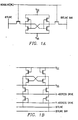
- FIGUREs 1A and 1B Schematics of two typical static random access memory (SRAM) are shown in FIGUREs 1A and 1B.
- the cell in FIGURE 1A is called a six transistor (6T) SRAM cell and comprises a pair of cross-coupled inverters to store a data bit state and pair of pass transistors to read and write a data bit between the cross-coupled inverters and a pair of bitlines.
- the bus which connects the pass transistor gates is called a wordline.
- the wordline connected to its pass transistor gates is activated to turn on the pass transistors.
- the cell in FIGURE 1B is an eight transistor (8T) SRAM cell and comprises a pair of cross-coupled inverters to store a data bit state and a pair of two transistors in series between the output nodes of the cross-coupled inverters and a pair of bitlines.
- the two transistors in series between the output of an inverter and a bitline are also called an X-pass transistor and a Y-pass transistor.
- the X-pass transistors have their gates connected to a row select bus running in the X-direction called an X-address drive and the Y-pass transistors have their gates connected to a column select bus called a Y-address drive running in the Y-direction.
- X-address and Y-address drives must be turned ON.
- DC characteristics of a static random access memory (SRAM) cell are determined by three parameters - read current, bitline write voltage (i.e. trip voltage), and static noise margin.
- the static noise margin reflects upon the cell stability against noise in the circuit during a read operation.
- a relatively high noise margin is a desired feature of a static random access memory cell.
- obtaining a good static noise margin is difficult because the threshold voltages of the transistors within a cell are kept low to maintain a certain level of drive current for the transistors.
- the static noise margin can be increased by increasing the beta ratio of a cell.
- the beta ratio for a 6T cell is defined as the ratio of the drive currents for the driver (pull-down) transistor to that for the pass transistor when they have the same threshold voltage.
- the beta ratio is defined as the ratio of the drive current for the driver transistor to that for the series of combination of the X-pass and Y-pass transistors.
- the beta ratio is also the same as the width ratio of the driver and the pass transistors if they have the same gate length and threshold voltage.
- a disadvantage of a high beta ratio is that it is difficult to write into a cell because an increase in the beta ratio lowers the bitline write voltage for the cell. This problem becomes more severe as the supply voltage Vcc is reduced for low voltage and or low power applications. Typically, a voltage below 1.5V is considered a low voltage implementation. Therefore, it is desirable to increase the beta ratio of the memory cell without adversely affecting its write capability.
- a need has arisen for a memory cell with an increased static noise margin without adversely affecting its write capability.
- a low voltage, low power SRAM cell is provided that substantially eliminates or reduces disadvantages and problems associated with conventional SRAM cell designs.
- a ten transistor (10T) low voltage, low power static random access memory cell that includes a first inverter having a first pull-up transistor connected between a first inverter output node and a Vcc or supply node, and a first pull-down transistor connected between the first inverter output node and a Vss or ground node.
- a typical transistor has at least three terminals - a source, a drain, and a gate. When it is said that a transistor is connected between two nodes, it means the transistor source is connected to one of the nodes and the transistor drain is connected to the other node.
- the cell also has a first pass transistor connected between the output node of the first inverter and a first pass node.
- a first bitline select transistor is connected between the first pass node and a first bitline.
- a first write pass transistor is also connected in parallel to the first pass transistor between the first pass node and the output node of the first inverter.
- the cell also includes a second inverter having a second pull-up transistor connected between a second inverter output node and the Vcc, and a second pull-down transistor connected between the second inverter output node and the Vss.
- a second pass transistor is connected between the second inverter output node and a second pass node.
- a second bitline select transistor is connected between the second pass node and a second bitline also called bitline bar.
- a second write pass transistor is also connected in parallel with the second pass transistor between the second pass node and the second inverter output node.
- the first and second inverters are cross-coupled by connecting the output of the first inverter with the input of the second inverter and connecting the output of the second inverter with the input of the first inverter.
- the bitline select transistors are turned ON. During the read operation only the pass transistors are turned ON and the write pass transistors are kept OFF, whereas during the write operation the pass and write pass transistors are turned ON.
- Embodiments of the invention provide technical advantages over conventional static random access memory cell devices.
- one technical advantage is the use of an extra write pass transistor to alter the DC characteristics of the SRAM.
- a narrower width for the pass transistor and keeping the write pass transistor OFF during read a high beta ratio is achieved to provide an increase in the static noise margin for the cell.
- the beta ratio of the cell is significantly reduced during the write operation, hence making it easier to write into the cell. If the write pass transistor width is significantly larger than that for the pass transistor, the pass transistor need not be turned ON during the write operation.
- the pass transistor can be used for the read operation and the write pass transistor can be used for the write operation.
- the 10T cell Unlike a 6T SRAM array where turning ON a wordline activates all the cells on that wordline, in the 10T cell only the addressed cell is activated, thereby reducing the power loss associated with accessing a cell. Activating a cell causes current to flow from the bitline to the Vss through the cell. Reducing the number of activated cells will reduce the power for the memory.
- the gates for the bitline select transistors are connected to the Y-address drive and the gates for the pass transistors and the write pass transistors obtain their signal from the X-address signal. The current in a cell only flows when 1) the bitline select transistors are turned ON and 2) pass transistors and or write pass transistors are turned ON.
- FIGURE 2 is a simplified schematic diagram of a ten transistor low voltage, low power SRAM memory cell 10.
- Low voltage, low power SRAM cell 10 includes a first inverter 12 having a first pull-up transistor 14 between a high end of the supply voltage node, Vcc, and a first inverter output node 13.
- First inverter 12 also has a first pull-down transistor 16 connected between output node 13 and a low end of the supply voltage node, Vss.
- the SRAM cell 10 also includes a second inverter 18 having a second pull-up transistor 20 and a second pull-down transistor 22.
- Second pull-up transistor 20 is connected between the Vcc and an output node 17 of second inverter 18.
- Second pull-down transistor is connected between output node 17 and the Vss.
- the two inverters are cross-coupled, i.e., output node 13 of first inverter 12 is connected to an input node 15 of second inverter 18 and output node 17 of the second inverter 18 is connected to an input node 19 of first inverter 12.
- a first pass transistor 24 is connected between output node 13 of first inverter 12 and a first pass node 35.
- a first bitline select transistor 28 is placed between first pass node 35 and a first bitline (Bitline) 36.
- a first write pass transistor 32 is also connected between first pass node 35 and output node 13 of first inverter 12.
- the cell also includes a second pass transistor 26 connected between output node 17 of second inverter 18 and a second pass node 37.
- a second bitline select transistor 30 is placed between second pass node 37 and a second bitline (also called Bitline Bar) 38.
- a second write pass transistor 34 is also connected between second pass node 37 and output node 17 of second inverter 18.
- the gates of pass transistors 24 and 26 are connected to a bus called Wordline (WL), the gates for write pass transistors 32 and 34 are connected to a bus called Write Wordline (Write WL), and the gates for bitline select transistors 28 and 30 are connected to a bus called Bitline Select Transistor Line (BLSTL).
- WL Wordline
- Write Wordline Write Wordline
- BSSTL Bitline Select Transistor Line
- the signal for the Wordline and the Write Wordline are derived from the X-address, or row select
- the signal for the Bitline Select Transistor Line is derived from the Y-address, or column select.
- the Bitline Select Transistor Line runs perpendicular to the Wordline and the Write Wordline buses. That is, if the Wordline and Write Wordline buses are running in the X-direction, the Bitline Select Transistor Line will run in the Y-direction.
- the Bitline and Bitline Bar buses will also run in the Y-direction.
- the pull-down transistors have n-channel configurations and have twice the width of the pass transistors which are also of n-channel configuration.
- the pull-up transistors have p-channel configurations and have widths around 1 to 1.5 times the width for the pass transistors.
- the width of the bitline select transistors which have n-channel configurations are about 4 times that of the pass transistors and the width of the write pass transistors which have n-channel configurations are 1.5 times that of the pass transistors.
- the transistors may also have different threshold voltages. A lower threshold voltage for the bitline select transistors compared to that for the pass transistors is expected to increase the read current of a cell and make it easier to write into the cell.
- the SRAM cell can have the first bitline select transistor 28 connected between the output node 13 of the first inverter 12 and the first pass node 35.
- the parallel combination of the first pass transistor 24 and the first write pass transistor 32 is connected between the first pass node 35 and the first bitline 36.
- the second bitline select transistor 30 is connected between the output node 17 of the second inverter 18 and the second pass node 37.
- the parallel combination of the second pass transistor 26 and the second write pass transistor 34 is connected between the second pass node 37 and the second bitline 38.
- FIGURE 3 is a simplified schematic diagram showing another embodiment of a low voltage, low power SRAM cell 10.
- the cell includes a pair of cross-coupled inverters 12 and 18.
- a first pass transistor 24 is connected directly between output node 13 of first inverter 12 and first bitline 36 and a second pass transistor 26 is connected directly between output node 17 of second inverter 18 and second bitline 38.
- a series combination of first write pass transistor 32 and first bitline select transistor 28 is also connected between output node 13 of first inverter 12 and first bitline 36.
- a series combination of second write pass transistor 34 and second bitline select transistor 30 is placed between output node 17 of second inverter 18 and second bitline 38.
- the read operation is performed by turning ON the pass transistors and the write operation is performed by turning ON the write pass transistors and bitline select transistors.
- the pass transistors could also be turned ON to make it easier to write.
- SRAM cell 10 can have first write pass transistor 32 connected to first bitline 36 and first pass node 35, and first bitline select transistor 28 connected to first pass node 35 and output node 13 of first inverter 12.
- second write pass transistor 34 can be connected to second bitline 38 and second pass node 37, with second bitline select transistor 30 connected to second pass node 37 and second output node 17 of the second inverter 18.
- the pull-up and the pull-down transistors in the inverters have p-channel and n-channel configurations, respectively.
- a pull-up transistor could be replaced by a resistor as done in a four transistor, two resistor cell.
- the pull-up transistor can be built in a substrate along with the other transistors or it could be formed in a thin film polycrystalline silicon material (TFT).
- TFT thin film polycrystalline silicon material
- the substrate could be single crystalline bulk silicon, silicon on insulator, etc.
Applications Claiming Priority (2)
| Application Number | Priority Date | Filing Date | Title |
|---|---|---|---|
| US1501496P | 1996-04-08 | 1996-04-08 | |
| US15014 | 1996-04-08 |
Publications (3)
| Publication Number | Publication Date |
|---|---|
| EP0801397A2 true EP0801397A2 (fr) | 1997-10-15 |
| EP0801397A3 EP0801397A3 (fr) | 1998-07-29 |
| EP0801397B1 EP0801397B1 (fr) | 2003-09-03 |
Family
ID=21769085
Family Applications (1)
| Application Number | Title | Priority Date | Filing Date |
|---|---|---|---|
| EP97302367A Expired - Lifetime EP0801397B1 (fr) | 1996-04-08 | 1997-04-07 | Perfectionnements dans ou relatifs à des dispositifs de mémoire à semi-conducteur |
Country Status (5)
| Country | Link |
|---|---|
| EP (1) | EP0801397B1 (fr) |
| JP (1) | JPH1027476A (fr) |
| KR (1) | KR100500072B1 (fr) |
| DE (1) | DE69724499T2 (fr) |
| TW (1) | TW442790B (fr) |
Cited By (2)
| Publication number | Priority date | Publication date | Assignee | Title |
|---|---|---|---|---|
| GB2510828A (en) * | 2013-02-13 | 2014-08-20 | Surecore Ltd | Single wordline low-power SRAM cells |
| CN112687308A (zh) * | 2020-12-29 | 2021-04-20 | 中国科学院上海微系统与信息技术研究所 | 低功耗静态随机存储器单元以及存储器 |
Families Citing this family (10)
| Publication number | Priority date | Publication date | Assignee | Title |
|---|---|---|---|---|
| CN1087659C (zh) * | 1997-10-05 | 2002-07-17 | 中国科学院大连化学物理研究所 | 己内酰胺加氢制六亚甲基亚胺催化剂及其应用 |
| JP4895439B2 (ja) * | 2001-06-28 | 2012-03-14 | ルネサスエレクトロニクス株式会社 | スタティック型メモリ |
| JP2006209877A (ja) | 2005-01-28 | 2006-08-10 | Nec Electronics Corp | 半導体記憶装置 |
| JP2007172715A (ja) * | 2005-12-20 | 2007-07-05 | Fujitsu Ltd | 半導体記憶装置およびその制御方法 |
| US7336533B2 (en) | 2006-01-23 | 2008-02-26 | Freescale Semiconductor, Inc. | Electronic device and method for operating a memory circuit |
| US7675806B2 (en) | 2006-05-17 | 2010-03-09 | Freescale Semiconductor, Inc. | Low voltage memory device and method thereof |
| US7471544B2 (en) * | 2006-05-31 | 2008-12-30 | Kabushiki Kaisha Toshiba | Method and apparatus for avoiding cell data destruction caused by SRAM cell instability |
| US7489540B2 (en) | 2007-05-22 | 2009-02-10 | Freescale Semiconductor, Inc. | Bitcell with variable-conductance transfer gate and method thereof |
| JP2010277634A (ja) | 2009-05-28 | 2010-12-09 | Toshiba Corp | 半導体記憶装置 |
| US9799395B2 (en) * | 2015-11-30 | 2017-10-24 | Texas Instruments Incorporated | Sense amplifier in low power and high performance SRAM |
Citations (1)
| Publication number | Priority date | Publication date | Assignee | Title |
|---|---|---|---|---|
| US5422857A (en) * | 1989-11-21 | 1995-06-06 | Matsushita Electric Industrial Co., Ltd. | Semiconductor memory unit having overlapping addresses |
Family Cites Families (1)
| Publication number | Priority date | Publication date | Assignee | Title |
|---|---|---|---|---|
| KR960001866B1 (ko) * | 1993-05-21 | 1996-02-06 | 현대전자산업주식회사 | 고속 비트라인 센싱 에스램 |
-
1997
- 1997-04-07 EP EP97302367A patent/EP0801397B1/fr not_active Expired - Lifetime
- 1997-04-07 JP JP9088323A patent/JPH1027476A/ja active Pending
- 1997-04-07 KR KR1019970012718A patent/KR100500072B1/ko not_active IP Right Cessation
- 1997-04-07 DE DE69724499T patent/DE69724499T2/de not_active Expired - Lifetime
- 1997-04-14 TW TW086104741A patent/TW442790B/zh not_active IP Right Cessation
Patent Citations (1)
| Publication number | Priority date | Publication date | Assignee | Title |
|---|---|---|---|---|
| US5422857A (en) * | 1989-11-21 | 1995-06-06 | Matsushita Electric Industrial Co., Ltd. | Semiconductor memory unit having overlapping addresses |
Non-Patent Citations (1)
| Title |
|---|
| EILHARD HASELHOFF: "Ein MOS-Speicher und seine Schaltungstechnik" ELEKTRONIK., vol. 21, MUNCHEN DE, pages 263-264, XP002064954 * |
Cited By (4)
| Publication number | Priority date | Publication date | Assignee | Title |
|---|---|---|---|---|
| GB2510828A (en) * | 2013-02-13 | 2014-08-20 | Surecore Ltd | Single wordline low-power SRAM cells |
| GB2510828B (en) * | 2013-02-13 | 2015-06-03 | Surecore Ltd | Single wordline low-power SRAM cells |
| US9627062B2 (en) | 2013-02-13 | 2017-04-18 | Surecore Limited | SRAM cells |
| CN112687308A (zh) * | 2020-12-29 | 2021-04-20 | 中国科学院上海微系统与信息技术研究所 | 低功耗静态随机存储器单元以及存储器 |
Also Published As
| Publication number | Publication date |
|---|---|
| JPH1027476A (ja) | 1998-01-27 |
| EP0801397B1 (fr) | 2003-09-03 |
| TW442790B (en) | 2001-06-23 |
| KR100500072B1 (ko) | 2005-09-12 |
| EP0801397A3 (fr) | 1998-07-29 |
| KR970071827A (ko) | 1997-11-07 |
| DE69724499D1 (de) | 2003-10-09 |
| DE69724499T2 (de) | 2004-07-22 |
Similar Documents
| Publication | Publication Date | Title |
|---|---|---|
| US6091626A (en) | Low voltage, low power static random access memory cell | |
| US6560139B2 (en) | Low leakage current SRAM array | |
| US6259623B1 (en) | Static random access memory (SRAM) circuit | |
| US20190172528A1 (en) | Semiconductor device | |
| US5471421A (en) | Storage cell using low powered/low threshold CMOS pass transistors having reduced charge leakage | |
| US7400523B2 (en) | 8T SRAM cell with higher voltage on the read WL | |
| KR101227291B1 (ko) | Sram용 워드선 구동 회로 및 그를 위한 방법 | |
| US4623989A (en) | Memory with p-channel cell access transistors | |
| US7466581B2 (en) | SRAM design with separated VSS | |
| EP0801397B1 (fr) | Perfectionnements dans ou relatifs à des dispositifs de mémoire à semi-conducteur | |
| US6212094B1 (en) | Low power SRAM memory cell having a single bit line | |
| US5689471A (en) | Dummy cell for providing a reference voltage in a memory array | |
| EP0987714B1 (fr) | Appareil et méthode pour réseau de mémoire RAM statique | |
| US8339893B2 (en) | Dual beta ratio SRAM | |
| GB2308699A (en) | Method for driving word lines in semicnductor memory device | |
| US5517461A (en) | Semiconductor storage device having latch circuitry coupled to data lines for eliminating through-current in sense amplifier | |
| US5570312A (en) | SRAM cell using word line controlled pull-up NMOS transistors | |
| US5473562A (en) | Method and apparatus for minimizing power-up crowbar current in a retargetable SRAM memory system | |
| JPH08129891A (ja) | メモリセル回路 | |
| US5220532A (en) | Self-locking load structure for static ram | |
| JP3298123B2 (ja) | マルチポートsram | |
| JP2005141858A (ja) | 半導体メモリ装置 |
Legal Events
| Date | Code | Title | Description |
|---|---|---|---|
| PUAI | Public reference made under article 153(3) epc to a published international application that has entered the european phase |
Free format text: ORIGINAL CODE: 0009012 |
|
| AK | Designated contracting states |
Kind code of ref document: A2 Designated state(s): DE FR GB IT NL |
|
| PUAL | Search report despatched |
Free format text: ORIGINAL CODE: 0009013 |
|
| AK | Designated contracting states |
Kind code of ref document: A3 Designated state(s): DE FR GB IT NL |
|
| 17P | Request for examination filed |
Effective date: 19980918 |
|
| 17Q | First examination report despatched |
Effective date: 20020108 |
|
| GRAH | Despatch of communication of intention to grant a patent |
Free format text: ORIGINAL CODE: EPIDOS IGRA |
|
| GRAH | Despatch of communication of intention to grant a patent |
Free format text: ORIGINAL CODE: EPIDOS IGRA |
|
| GRAA | (expected) grant |
Free format text: ORIGINAL CODE: 0009210 |
|
| AK | Designated contracting states |
Kind code of ref document: B1 Designated state(s): DE FR GB IT NL |
|
| PG25 | Lapsed in a contracting state [announced via postgrant information from national office to epo] |
Ref country code: NL Free format text: LAPSE BECAUSE OF FAILURE TO SUBMIT A TRANSLATION OF THE DESCRIPTION OR TO PAY THE FEE WITHIN THE PRESCRIBED TIME-LIMIT Effective date: 20030903 Ref country code: IT Free format text: LAPSE BECAUSE OF FAILURE TO SUBMIT A TRANSLATION OF THE DESCRIPTION OR TO PAY THE FEE WITHIN THE PRESCRIBED TIME-LIMIT;WARNING: LAPSES OF ITALIAN PATENTS WITH EFFECTIVE DATE BEFORE 2007 MAY HAVE OCCURRED AT ANY TIME BEFORE 2007. THE CORRECT EFFECTIVE DATE MAY BE DIFFERENT FROM THE ONE RECORDED. Effective date: 20030903 Ref country code: FR Free format text: LAPSE BECAUSE OF FAILURE TO SUBMIT A TRANSLATION OF THE DESCRIPTION OR TO PAY THE FEE WITHIN THE PRESCRIBED TIME-LIMIT Effective date: 20030903 |
|
| REG | Reference to a national code |
Ref country code: GB Ref legal event code: FG4D |
|
| REF | Corresponds to: |
Ref document number: 69724499 Country of ref document: DE Date of ref document: 20031009 Kind code of ref document: P |
|
| NLV1 | Nl: lapsed or annulled due to failure to fulfill the requirements of art. 29p and 29m of the patents act | ||
| PLBE | No opposition filed within time limit |
Free format text: ORIGINAL CODE: 0009261 |
|
| STAA | Information on the status of an ep patent application or granted ep patent |
Free format text: STATUS: NO OPPOSITION FILED WITHIN TIME LIMIT |
|
| 26N | No opposition filed |
Effective date: 20040604 |
|
| EN | Fr: translation not filed | ||
| PGFP | Annual fee paid to national office [announced via postgrant information from national office to epo] |
Ref country code: DE Payment date: 20130430 Year of fee payment: 17 |
|
| PGFP | Annual fee paid to national office [announced via postgrant information from national office to epo] |
Ref country code: GB Payment date: 20140325 Year of fee payment: 18 |
|
| REG | Reference to a national code |
Ref country code: DE Ref legal event code: R119 Ref document number: 69724499 Country of ref document: DE |
|
| PG25 | Lapsed in a contracting state [announced via postgrant information from national office to epo] |
Ref country code: DE Free format text: LAPSE BECAUSE OF NON-PAYMENT OF DUE FEES Effective date: 20141101 |
|
| REG | Reference to a national code |
Ref country code: DE Ref legal event code: R119 Ref document number: 69724499 Country of ref document: DE Effective date: 20141101 |
|
| GBPC | Gb: european patent ceased through non-payment of renewal fee |
Effective date: 20150407 |
|
| PG25 | Lapsed in a contracting state [announced via postgrant information from national office to epo] |
Ref country code: GB Free format text: LAPSE BECAUSE OF NON-PAYMENT OF DUE FEES Effective date: 20150407 |