EP0785561A2 - Composition diélectrique céramique et condensateur monolithique céramique utilisant celui-ci - Google Patents
Composition diélectrique céramique et condensateur monolithique céramique utilisant celui-ci Download PDFInfo
- Publication number
- EP0785561A2 EP0785561A2 EP97100644A EP97100644A EP0785561A2 EP 0785561 A2 EP0785561 A2 EP 0785561A2 EP 97100644 A EP97100644 A EP 97100644A EP 97100644 A EP97100644 A EP 97100644A EP 0785561 A2 EP0785561 A2 EP 0785561A2
- Authority
- EP
- European Patent Office
- Prior art keywords
- dielectric ceramic
- oxide
- nickel
- ceramic composition
- layers
- Prior art date
- Legal status (The legal status is an assumption and is not a legal conclusion. Google has not performed a legal analysis and makes no representation as to the accuracy of the status listed.)
- Granted
Links
Images
Classifications
-
- H—ELECTRICITY
- H01—ELECTRIC ELEMENTS
- H01G—CAPACITORS; CAPACITORS, RECTIFIERS, DETECTORS, SWITCHING DEVICES OR LIGHT-SENSITIVE DEVICES, OF THE ELECTROLYTIC TYPE
- H01G4/00—Fixed capacitors; Processes of their manufacture
- H01G4/002—Details
- H01G4/018—Dielectrics
- H01G4/06—Solid dielectrics
- H01G4/08—Inorganic dielectrics
- H01G4/12—Ceramic dielectrics
-
- C—CHEMISTRY; METALLURGY
- C04—CEMENTS; CONCRETE; ARTIFICIAL STONE; CERAMICS; REFRACTORIES
- C04B—LIME, MAGNESIA; SLAG; CEMENTS; COMPOSITIONS THEREOF, e.g. MORTARS, CONCRETE OR LIKE BUILDING MATERIALS; ARTIFICIAL STONE; CERAMICS; REFRACTORIES; TREATMENT OF NATURAL STONE
- C04B35/00—Shaped ceramic products characterised by their composition; Ceramics compositions; Processing powders of inorganic compounds preparatory to the manufacturing of ceramic products
- C04B35/01—Shaped ceramic products characterised by their composition; Ceramics compositions; Processing powders of inorganic compounds preparatory to the manufacturing of ceramic products based on oxide ceramics
- C04B35/46—Shaped ceramic products characterised by their composition; Ceramics compositions; Processing powders of inorganic compounds preparatory to the manufacturing of ceramic products based on oxide ceramics based on titanium oxides or titanates
- C04B35/462—Shaped ceramic products characterised by their composition; Ceramics compositions; Processing powders of inorganic compounds preparatory to the manufacturing of ceramic products based on oxide ceramics based on titanium oxides or titanates based on titanates
- C04B35/465—Shaped ceramic products characterised by their composition; Ceramics compositions; Processing powders of inorganic compounds preparatory to the manufacturing of ceramic products based on oxide ceramics based on titanium oxides or titanates based on titanates based on alkaline earth metal titanates
- C04B35/468—Shaped ceramic products characterised by their composition; Ceramics compositions; Processing powders of inorganic compounds preparatory to the manufacturing of ceramic products based on oxide ceramics based on titanium oxides or titanates based on titanates based on alkaline earth metal titanates based on barium titanates
-
- C—CHEMISTRY; METALLURGY
- C04—CEMENTS; CONCRETE; ARTIFICIAL STONE; CERAMICS; REFRACTORIES
- C04B—LIME, MAGNESIA; SLAG; CEMENTS; COMPOSITIONS THEREOF, e.g. MORTARS, CONCRETE OR LIKE BUILDING MATERIALS; ARTIFICIAL STONE; CERAMICS; REFRACTORIES; TREATMENT OF NATURAL STONE
- C04B35/00—Shaped ceramic products characterised by their composition; Ceramics compositions; Processing powders of inorganic compounds preparatory to the manufacturing of ceramic products
- C04B35/01—Shaped ceramic products characterised by their composition; Ceramics compositions; Processing powders of inorganic compounds preparatory to the manufacturing of ceramic products based on oxide ceramics
- C04B35/495—Shaped ceramic products characterised by their composition; Ceramics compositions; Processing powders of inorganic compounds preparatory to the manufacturing of ceramic products based on oxide ceramics based on vanadium, niobium, tantalum, molybdenum or tungsten oxides or solid solutions thereof with other oxides, e.g. vanadates, niobates, tantalates, molybdates or tungstates
-
- H—ELECTRICITY
- H01—ELECTRIC ELEMENTS
- H01G—CAPACITORS; CAPACITORS, RECTIFIERS, DETECTORS, SWITCHING DEVICES OR LIGHT-SENSITIVE DEVICES, OF THE ELECTROLYTIC TYPE
- H01G4/00—Fixed capacitors; Processes of their manufacture
- H01G4/002—Details
- H01G4/018—Dielectrics
- H01G4/06—Solid dielectrics
- H01G4/08—Inorganic dielectrics
- H01G4/12—Ceramic dielectrics
- H01G4/1209—Ceramic dielectrics characterised by the ceramic dielectric material
- H01G4/1218—Ceramic dielectrics characterised by the ceramic dielectric material based on titanium oxides or titanates
- H01G4/1227—Ceramic dielectrics characterised by the ceramic dielectric material based on titanium oxides or titanates based on alkaline earth titanates
-
- H—ELECTRICITY
- H01—ELECTRIC ELEMENTS
- H01G—CAPACITORS; CAPACITORS, RECTIFIERS, DETECTORS, SWITCHING DEVICES OR LIGHT-SENSITIVE DEVICES, OF THE ELECTROLYTIC TYPE
- H01G4/00—Fixed capacitors; Processes of their manufacture
- H01G4/002—Details
- H01G4/018—Dielectrics
- H01G4/06—Solid dielectrics
- H01G4/08—Inorganic dielectrics
- H01G4/12—Ceramic dielectrics
- H01G4/1209—Ceramic dielectrics characterised by the ceramic dielectric material
- H01G4/1254—Ceramic dielectrics characterised by the ceramic dielectric material based on niobium or tungsteen, tantalum oxides or niobates, tantalates
Definitions
- the present invention relates to a dielectric ceramic composition and use of the dielectric ceramic composition for a monolithic ceramic capacitor, especially for a monolithic ceramic capacitor provided with internal electrodes of nickel or nickel alloy.
- the above-mentioned first composition (which is a non-reducible dielectric ceramic composition) suffers the disadvantage that CaZrO 3 and CaTiO 2 (which form during firing) combine with Mn to cause heterogeneity. This poses a problem with decrease in reliability at high temperatures.
- the above-mentioned second composition (which is a non-reducible dielectric ceramic composition) suffers the disadvantage that its insulation resistance and capacity are greatly affected by the grain size of BaTiO 3 as the principal component. This causes difficulties in producing stable characteristic properties. In addition, it has an unpractically low CR value of 1000-2000 ⁇ F (which is a product of insulation resistance and electrostatic capacity).
- the above-mentioned third composition suffers the disadvantage of giving rise to a dielectric material having a permittivity of 2000-2800, which is inferior to conventional compositions containing precious metal (such as palladium) which have a permittivity of 3000-3500. Therefore, it will not meet the requirement for capacitors having a smaller size and a large capacity if it is used to replace conventional materials only for cost reduction.
- non-reducible dielectric ceramic compositions proposed so far suffer the disadvantage of greatly decreasing in resistance at high temperatures (although they have high insulation resistance at room temperature). Decrease in resistance occurs remarkably especially in a strong electric field. This is a great hindrance to the reduction of thickness of dielectric layers. This is the reason why there has been no practical thin-layer laminated capacitors made of non-reducible dielectric ceramic compositions.
- the present invention provides a dielectric ceramic composition which comprises a primary component and a secondary component in a molar ratio of from 100/0.5 to 100/5.0 and an auxiliary component in an amount of from 0.2 to 3.0 parts by weight for 100 parts by weight in total of said primary and secondary components, said primary component being composed of barium titanate (containing less than 0.02 wt% of alkali metal oxide as an impurity), scandium oxide, yttrium oxide, samarium oxide, europium oxide, manganese oxide, cobalt oxide, and nickel oxide, as expressed by the compositional formula below: (1 - ⁇ - ⁇ - ⁇ ) ⁇ BaO ⁇ m ⁇ TiO 2 + ⁇ M 2 O 3 + ⁇ Re 2 O 3 + ⁇ (Mn 1-x-y Ni x Co y )O (where M 2 O 3 denotes Sc 2 O 3 or Y 2 O 3 or both, Re 2 O 3 denotes Sm 2 O 3 or Eu 2 O 3 or both, ⁇ ,
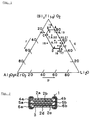
- the present invention further provides a dielectric ceramic composition as defined above, wherein said auxiliary component is represented by the general formula of pLi 2 O-q(Si z Ti 1-z )O 2 -rM (where p, q, and r denote the mol% of the respective constituents, z is defined by 0.30 ⁇ z ⁇ 1.0, M stands for Al 2 O 3 or ZrO 2 or both, and p, q, and r are within the area enclosed by the polygon having apexes defined as follows in the triangular coordinates:
- the present invention further provides a use of the above described dielectric ceramic compositions for a monolithic ceramic capacitor comprising; a plurality of dielectric ceramic layers made from said dielectric ceramic composition, a plurality of internal electrodes made from nickel or nickel alloy formed between said dielectric ceramic layers.
- the above described internal electrodes show their edges from the ends of the dielectric ceramic layers, and external electrodes are electrically connected to the edges of said internal electrodes.
- the above described external electrodes are constructed of sintered layers of electrically conductive metal powder containing or not containing glass frit.
- the above described sintered layers have a plated layer thereon.
- barium titanate BaTiO 3
- Table 1 Four kinds of barium titanate (BaTiO 3 ) as shown in Table 1 were prepared from TiCl 4 and Ba(NO 3 ) 2 (both varying in purity) in prescribed amounts by precipitation in the form of titanylbarium oxalate (BaTiO(C 2 O 4 ) ⁇ 4H 2 O) with oxalic acid, followed by pyrolysis at 1000°C or above.
- a powder was prepared from oxides, carbonates, and hydroxides of respective components for the compositional formula 0.25 Li 2 O-0.65 (0.30 TiO 2 ⁇ 0.70 SiO 2 )-0.10 Al 2 O 3 (in molar ratio) by mixing, crushing, evaporation, and drying. This powder was made into an oxide glass powder having an average grain size smaller than 1 ⁇ m by melting at 1300°C, quenching, and crushing.
- Each sample in powder form was prepared by mixing from barium titanate (prepared as mentioned above), BaCO 3 (to adjust the Ba/Ti molar ratio m in barium titanate), oxide glass powder (prepared as mentioned above), and Sc 2 O 3 , Y 2 O 3 , Sm 2 O 3 , Eu 2 O 3 , MnCO 3 , NiO, Co 2 O 3 , and MgO, all of which have a purity higher than 99%, as much as necessary to conform to the compositional formula shown in Table 2.
- the powder mixture obtained as mentioned above was mixed with a binder (polyvinyl butyral) and an organic solvent (ethanol) by wet ball-milling to give a ceramics slurry.
- a binder polyvinyl butyral
- ethanol organic solvent
- the slurry was made into a rectangular ceramics green sheet, 11 ⁇ m thick.
- the green sheet was coated with a nickel-based conductive paste by printing, so as to form a conductive paste layer which becomes the internal electrode afterward.
- the sintered body had its both ends coated with a silver paste, which was subsequently baked at 600°C in a nitrogen atmosphere. This step formed external electrodes (electrically connected to internal electrodes). Thus there was obtained a monolithic ceramic capacitor.
- the thus obtained monolithic ceramic capacitor measures 1.6 mm wide, 3.2 mm long, and 1.2 mm thick, and the dielectric ceramic layer held between the internal electrodes is 8 ⁇ m thick.
- the effective dielectric ceramic layers count 19, and the area of opposed electrodes for each layer is 2.1 mm 2 .
- the monolithic ceramic capacitor was tested for the following characteristic properties.
- Humidity resistance under load was tested (on 72 specimens for each test) by measuring the change with time in insulation resistance that occurred when a DC voltage of 16V was applied at 121°C and 2 atmospheric pressure (100% RH). The results are expressed in terms of the number of the defective specimens which decreased in insulation resistance (R) below 10 6 ⁇ within 250 hours.
- the monolithic ceramic capacitors pertaining to the present invention have a permittivity ( ⁇ ) higher than 3000, a dielectric loss tangent (tan ⁇ ) lower than 2.5%, and a rate of change with temperature in electrostatic capacity that meets the B specification prescribed in JIS in the temperature range from -25°C to 85°C and also meets the X7R specification prescribed in EIA in the temperature range from -55°C to 125°C.
- the samples pertaining to the present invention have a high insulation resistance measured for 16V and 160V at 25°C which is evidenced by the respective CR products of 6000 ⁇ F and 2000 ⁇ F. They also have a high insulation resistance measured for 16V and 160V at 125°C which is evidenced by the respective CR products of 2000 ⁇ F and 500 ⁇ F. They have an average life longer than 500 hours and pass the humidity load test. They can be formed by sintering at comparatively low temperatures (1300°C or below).
- compositional variables specified in the present invention are based on the following experimental facts.
- Sample No. 1 in which the amount ( ⁇ + ⁇ ) of (M 2 O 3 + Re 2 O 3 ) is less than 0.0025, has a permittivity ( ⁇ ) lower than 3000, a dielectric loss tangent (tan ⁇ ) higher than 2.5%, a high rate of change with time in electrostatic capacity, and an extremely short life.
- Sample No. 19 in which the amount ( ⁇ + ⁇ ) of (M 2 O 3 + Re 2 O 3 ) is more than 0.025, has a permittivity ( ⁇ ) lower than 3000, a low insulation resistance, and a short average life. In addition, it needs a high sintering temperature and gives rise to some defectives in the humidity load test.
- Sample No. 2 in which the amount ( ⁇ ) of (Mn, Ni, Co)O is less than 0.0025, is subject to reduction during firing in a reducing atmosphere. This reduction changes the ceramics into a semiconductor, thereby decreasing its insulation resistance (which is undesirable).
- Sample No. 3 in which the value of b is 0, has an average life shorter than 500 hours.
- Sample No. 21 in which the ratio ⁇ /( ⁇ + ⁇ ) exceeds 4, has a high rate of change with temperature in electrostatic capacity (which is not desirable).
- Samples Nos. 4 and 5 in which the molar ratio (m) of barium titanate is smaller than or equal to 1.000, is subject to change into semiconductor and has a low insulation resistance and an average life shorter than 500 hours.
- Sample No. 6 in which the amount of MgO is less than 0.5 mole, has an insulation resistance lower than 2000 ⁇ F (at 25°C and 160V) and an average life shorter than 500 hours. In addition, it has a rate of change with temperature in electrostatic capacity which does not meet the B specification of JIS and the X7R specification of EIA.
- Sample No. 27 in which the amount of MgO exceeds 5 moles, needs a high sintering temperature, has a permittivity lower than 3000, is poor in insulation resistance, and fails the humidity load test.
- Sample No. 7 in which the amount of oxide glass is less than 0.2 parts by weight, is not completely sintered even at 1350°C.
- Sample No. 28 in which the amount of oxide glass exceeds 3.0 parts by weight, has a low permittivity and a high rate of change with temperature in electrostatic capacity.
- Sample No. 29 in which the amount of alkali metal (as an impurity in barium titanate) exceeds 0.02 parts by weight, has a low permittivity.
- ratio ⁇ / ⁇ is not particularly specified, it should desirably be smaller than or equal to 1 so that the samples have a rate of change with temperature in electrostatic capacity which meets the specification with a margin.
- a powder of dielectric material was prepared from barium titanate (designated as A in Table 1) and respective starting materials in such amounts as specified below. 97.3 ⁇ BaO ⁇ 1.010 ⁇ TiO 2 + 0.6 Y 2 O 3 + 0.1 Sm 2 O 3 + 0.6 MnO + 0.6 NiO + 0.8 CoO (in molar ratio). This powder was incorporated with 1.2 moles of MgO. The thus prepared raw material was incorporated with an oxide glass (having an average particle size smaller than 1 ⁇ m) as shown in Table 4). This oxide glass was prepared in the same manner as in Example 1. The resulting dielectric ceramic composition was made into monolithic ceramic capacitors in the same manner as in Example 1.
- the monolithic ceramic capacitor has internal electrodes and silver external electrodes electrically connected to the internal electrodes.
- the glass melting temperature was adjusted in the range of 1200-1500°C according to the glass composition.
- Table 4 Sample No. Amount of glass (wt%) Components of oxide glass (wt%) Li 2 O Si z Ti 1-z z Al 2 O 3 ZrO 3 1 1.00 20 80 0.3 0 0 2 0.80 10 80 0.6 5 5 3 1.00 10 70 0.5 20 0 4 1.00 35 45 1.0 10 10 5 1.20 45 45 0.5 10 0 6 1.00 45 55 0.3 0 0 7 0.80 20 70 0.6 5 5 8 1.00 20 70 0.4 10 0 9 1.00 30 60 0.7 5 5 10 0.80 30 60 0.8 10 0 11 1.50 40 50 0.6 5 5 12 2.00 40 50 0.9 0 10 13* 1.20 10 85 0.4 5 0 14* 1.50 5 75 0.6 10 10 15* 1.00 20 55 0.5 25 0 16* 1.20 45 40 0.8 0 15 17
- composition of the oxide glass is defined by the triangular coordinates shown in Fig. 1.
- the monolithic ceramic capacitors in this example have the same dimensions as those in Example 1.
- the monolithic ceramic capacitors were tested for electrical properties as follows:
- Humidity resistance under load was tested (on 72 specimens for each test) by measuring the change with time in insulation resistance that occurred when a DC voltage of 16V was applied at 121°C and 2 atmospheric pressure (100% RH). The results are expressed in terms of the number of the defective specimens which decreased in insulation resistance (R) below 10 6 ⁇ within 250 hours.
- the monolithic ceramic capacitors composed of dielectric ceramic layers containing the oxide glass specified in the present invention have a permittivity ( ⁇ ) higher than 3000, a dielectric loss tangent (tan ⁇ ) lower than 2.5%, and a rate of change with temperature in electrostatic capacity that meets the X7R specification prescribed in EIA in the temperature range from -55°C to 125°C.
- the samples pertaining to the present invention have a high insulation resistance measured for 16V and 160V at 25°C which is evidenced by the respective CR products of 6000 ⁇ F and 2000 ⁇ F. They also have a high insulation resistance measured for 16V and 160V at 125°C which is evidenced by the respective CR products of 2000 ⁇ F and 500 ⁇ F. They have an average life longer than 500 hours and pass the humidity load test. They can be formed by sintering at comparatively low temperatures (1300°C or below).
- Fig. 2 is a sectional view showing the monolithic ceramic capacitor pertaining to the present invention.
- the monolithic ceramic capacitor 1 is composed of dielectric ceramic layers 3 and internal electrodes 2a, 2b, 2c, and 2d, which are placed alternately on top of the other.
- the monolithic ceramic capacitor 1 has external electrodes 4a and 4b which are electrically connected to the internal electrodes 2a, 2b, 2c, and 2d.
- the external electrodes 4a and 4b have another external electrodes 5a and 5b of nickel or copper formed thereon by plating.
- the external electrodes 5a and 5b have another external electrodes 6a and 6b of solder or tin formed thereon by plating.
- the monolithic ceramic capacitor 1 can be obtained by the manufacturing process mentioned in Example 1 or 2.
- the one shown in Fig. 2 has the external electrodes of three-layer structure; however, the external electrodes may be of single-layer structure or multi-layer structure depending on the usage of the capacitor.
- barium titanate in powder form prepared from the oxalic acid method was used in the above-mentioned examples, it may be replaced by the one prepared by the alkoxide method or hydrothermal method so as to improve the characteristic properties of the monolithic ceramic capacitor.
- yttrium, cobalt, and nickel may be used in the form of alkoxide solution or organometal solution in place of oxide powder without any adverse effect of the characteristic properties so long as they are used in specified amounts for the dielectric ceramic composition.
- the internal electrodes may be formed by any of screen printing, vacuum deposition, and plating.
- the external electrodes may be formed from the same material as used for the internal electrodes. It may also be formed from silver, palladium, or silver-palladium alloy, which may be adequately selected depending on the usage of the monolithic ceramic capacitor.
- the external electrodes were formed by coating with metal powder paste and subsequent baking after firing. Alternatively, they may be formed by coating prior to firing and subsequent baking simultaneous with the firing of the monolithic ceramic capacitor.
- the external electrodes of silver may also be coated sequentially with a layer of nickel or copper and a layer of solder or tin which are formed by plating.
- the dielectric ceramics capacitor can be formed by firing at 1260-1300°C in a neutral or reducing atmosphere. Yet, it has an insulation resistance and an electrostatic capacity such that their product (CR product) is higher than 6000 ⁇ F. This value changes only a little even in a high electric field. It has a high rated voltage with high reliability and exhibits a permittivity higher than 3000 even though the dielectric ceramic layers are made thinner.
- the dielectric ceramic composition of the present invention can be made into monolithic ceramic capacitors which have the above-mentioned characteristic properties and the temperature-dependent electrostatic capacity which meets the B specification of JIS and the X7R specification of EIA. These outstanding properties remain unchanged even at high temperatures under high humidity.
- the monolithic ceramic capacitor of the present invention has internal electrodes of nickel or nickel alloy. Therefore, it is less expensive than the conventional one that has internal electrodes of precious metal such as palladium. Yet, it exhibits good weather-resistance performance such as load characteristics at high temperatures under high humidity.
Landscapes
- Engineering & Computer Science (AREA)
- Chemical & Material Sciences (AREA)
- Ceramic Engineering (AREA)
- Power Engineering (AREA)
- Manufacturing & Machinery (AREA)
- Microelectronics & Electronic Packaging (AREA)
- Inorganic Chemistry (AREA)
- Organic Chemistry (AREA)
- Structural Engineering (AREA)
- Materials Engineering (AREA)
- Compositions Of Oxide Ceramics (AREA)
- Inorganic Insulating Materials (AREA)
- Ceramic Capacitors (AREA)
Applications Claiming Priority (9)
| Application Number | Priority Date | Filing Date | Title |
|---|---|---|---|
| JP653096 | 1996-01-18 | ||
| JP653096 | 1996-01-18 | ||
| JP6530/96 | 1996-01-18 | ||
| JP61357/96 | 1996-03-18 | ||
| JP6135796 | 1996-03-18 | ||
| JP6135796 | 1996-03-18 | ||
| JP8291998A JP3039397B2 (ja) | 1996-01-18 | 1996-11-01 | 誘電体磁器組成物とそれを用いた積層セラミックコンデンサ |
| JP291998/96 | 1996-11-01 | ||
| JP29199896 | 1996-11-01 |
Publications (3)
| Publication Number | Publication Date |
|---|---|
| EP0785561A2 true EP0785561A2 (fr) | 1997-07-23 |
| EP0785561A3 EP0785561A3 (fr) | 1997-09-24 |
| EP0785561B1 EP0785561B1 (fr) | 2001-04-18 |
Family
ID=27277204
Family Applications (1)
| Application Number | Title | Priority Date | Filing Date |
|---|---|---|---|
| EP97100644A Expired - Lifetime EP0785561B1 (fr) | 1996-01-18 | 1997-01-16 | Composition diélectrique céramique et son utilisation dans un condensateur monolithique céramique |
Country Status (6)
| Country | Link |
|---|---|
| US (1) | US5801111A (fr) |
| EP (1) | EP0785561B1 (fr) |
| JP (1) | JP3039397B2 (fr) |
| KR (1) | KR100231798B1 (fr) |
| CN (1) | CN1090371C (fr) |
| DE (1) | DE69704580T2 (fr) |
Cited By (5)
| Publication number | Priority date | Publication date | Assignee | Title |
|---|---|---|---|---|
| EP0924721A1 (fr) * | 1997-12-19 | 1999-06-23 | Kabushiki Kaisha Toshiba | Composition céramique diélectrique, condensateur multicouche et son procédé de fabrication |
| EP0977217A1 (fr) * | 1998-05-12 | 2000-02-02 | Murata Manufacturing Co., Ltd. | Composition diélectrique céramique et condensateur céramique multicouche |
| GB2369354A (en) * | 2000-10-24 | 2002-05-29 | Murata Manufacturing Co | Dielectric ceramic, process for producing the same and multilayer ceramic capacitor |
| EP1235236A1 (fr) * | 1996-08-05 | 2002-08-28 | Murata Manufacturing Co., Ltd. | Composition diélectrique céramique et condensateur céramique utilisant celle-ci |
| DE10000588B4 (de) * | 1999-01-18 | 2011-04-14 | Murata Mfg. Co., Ltd., Nagaokakyo-shi | Verfahren zum Sortieren von monolithischen Keramikkondensatoren |
Families Citing this family (26)
| Publication number | Priority date | Publication date | Assignee | Title |
|---|---|---|---|---|
| JP3039417B2 (ja) * | 1997-02-07 | 2000-05-08 | 株式会社村田製作所 | 積層セラミックコンデンサ |
| EP0913843B1 (fr) * | 1997-03-31 | 2006-02-08 | TDK Corporation | Materiau ceramique dielectrique non reducteur |
| JP3334606B2 (ja) * | 1997-07-23 | 2002-10-15 | 株式会社村田製作所 | 誘電体磁器組成物および積層セラミックコンデンサ |
| SG65086A1 (en) * | 1997-07-23 | 1999-05-25 | Murata Manufacturing Co | Dielectric ceramic composition and monolithic ceramic capacitor using same |
| JP3644235B2 (ja) * | 1998-03-03 | 2005-04-27 | 株式会社村田製作所 | 積層セラミック電子部品 |
| US6243254B1 (en) * | 1998-08-11 | 2001-06-05 | Murata Manufacturing Co., Ltd. | Dielectric ceramic composition and laminated ceramic capacitor using the same |
| JP2000072540A (ja) * | 1998-08-31 | 2000-03-07 | Ngk Spark Plug Co Ltd | 誘電体材料 |
| US6074971A (en) * | 1998-11-13 | 2000-06-13 | The United States Of America As Represented By The Secretary Of The Army | Ceramic ferroelectric composite materials with enhanced electronic properties BSTO-Mg based compound-rare earth oxide |
| GB2384502B (en) * | 1998-11-16 | 2004-10-13 | Shell Oil Co | Coupling an expandable tubular member to a preexisting structure |
| JP3606079B2 (ja) * | 1998-12-25 | 2005-01-05 | 株式会社村田製作所 | 非直線性誘電体磁器、パルス発生用コンデンサ、高圧蒸気放電灯回路および高圧蒸気放電灯 |
| JP2000357624A (ja) * | 1999-06-16 | 2000-12-26 | Murata Mfg Co Ltd | 積層セラミック電子部品 |
| US6556422B2 (en) * | 2000-07-05 | 2003-04-29 | Samsung Electro-Mechanics Co., Ltd. | Dielectric ceramic composition, multi-layer ceramic capacitor using the same, and manufacturing method therefor |
| JP2002050536A (ja) * | 2000-07-31 | 2002-02-15 | Murata Mfg Co Ltd | 耐還元性誘電体セラミックおよび積層セラミックコンデンサ |
| JP3864114B2 (ja) * | 2001-08-02 | 2006-12-27 | 株式会社日本自動車部品総合研究所 | 積層型誘電体の製造方法 |
| JP5153288B2 (ja) * | 2002-01-15 | 2013-02-27 | Tdk株式会社 | 誘電体磁器組成物および電子部品 |
| KR100495210B1 (ko) * | 2002-07-05 | 2005-06-14 | 삼성전기주식회사 | 내환원성 저온소성 유전체 자기조성물, 이를 이용한적층세라믹 커패시터 및 그 제조방법 |
| KR100471155B1 (ko) * | 2002-12-03 | 2005-03-10 | 삼성전기주식회사 | 저온소성 유전체 자기조성물과 이를 이용한 적층세라믹커패시터 |
| US6828266B1 (en) * | 2003-05-16 | 2004-12-07 | Ferro Corporation | X7R dielectric composition |
| CN100403467C (zh) * | 2003-08-08 | 2008-07-16 | 广东风华高新科技股份有限公司 | 多层陶瓷电容器及其制备方法与所用的介电陶瓷材料 |
| JP2005136132A (ja) * | 2003-10-30 | 2005-05-26 | Tdk Corp | 積層コンデンサ |
| JP5297011B2 (ja) * | 2007-07-26 | 2013-09-25 | 太陽誘電株式会社 | 積層セラミックコンデンサ及びその製造方法 |
| JP4798231B2 (ja) * | 2009-01-30 | 2011-10-19 | 株式会社村田製作所 | 誘電体セラミックおよび積層セラミックコンデンサ |
| TW201107267A (en) * | 2009-08-21 | 2011-03-01 | Darfon Electronics Corp | Ceramic powder composition, ceramic material and laminated ceramic capacitor made of the same |
| US8178458B2 (en) * | 2009-12-01 | 2012-05-15 | National Taiwan University Technology | Dielectric ceramic composition |
| JP6093797B2 (ja) * | 2015-03-31 | 2017-03-08 | 株式会社アールシーコア | 屋根の防湿構造 |
| CN106007672B (zh) * | 2016-05-18 | 2018-07-31 | 湖南圣瓷科技有限公司 | 一种电力用绝缘陶瓷的制备方法及其绝缘陶瓷和应用 |
Citations (4)
| Publication number | Priority date | Publication date | Assignee | Title |
|---|---|---|---|---|
| JPS60103861A (ja) | 1983-11-11 | 1985-06-08 | Matsushita Electric Ind Co Ltd | テレビ電話 |
| JPS6114610A (ja) | 1984-06-29 | 1986-01-22 | Fujitsu Ltd | 光コネクタ部品と光フアイバの接続方法 |
| JPH059068A (ja) | 1991-06-27 | 1993-01-19 | Murata Mfg Co Ltd | 非還元性誘電体磁器組成物 |
| JPH059066A (ja) | 1991-06-27 | 1993-01-19 | Murata Mfg Co Ltd | 非還元性誘電体磁器組成物 |
Family Cites Families (2)
| Publication number | Priority date | Publication date | Assignee | Title |
|---|---|---|---|---|
| EP0476143B1 (fr) * | 1990-03-28 | 1995-01-04 | TAIYO YUDEN Co., Ltd. | Condensateur en ceramique et production de ce condensateur |
| JP3269910B2 (ja) * | 1994-03-30 | 2002-04-02 | 太陽誘電株式会社 | 磁器コンデンサ及びその製造方法 |
-
1996
- 1996-11-01 JP JP8291998A patent/JP3039397B2/ja not_active Expired - Lifetime
-
1997
- 1997-01-16 EP EP97100644A patent/EP0785561B1/fr not_active Expired - Lifetime
- 1997-01-16 DE DE69704580T patent/DE69704580T2/de not_active Expired - Lifetime
- 1997-01-16 CN CN97102285A patent/CN1090371C/zh not_active Expired - Lifetime
- 1997-01-17 KR KR1019970001289A patent/KR100231798B1/ko not_active IP Right Cessation
- 1997-01-21 US US08/785,783 patent/US5801111A/en not_active Expired - Lifetime
Patent Citations (4)
| Publication number | Priority date | Publication date | Assignee | Title |
|---|---|---|---|---|
| JPS60103861A (ja) | 1983-11-11 | 1985-06-08 | Matsushita Electric Ind Co Ltd | テレビ電話 |
| JPS6114610A (ja) | 1984-06-29 | 1986-01-22 | Fujitsu Ltd | 光コネクタ部品と光フアイバの接続方法 |
| JPH059068A (ja) | 1991-06-27 | 1993-01-19 | Murata Mfg Co Ltd | 非還元性誘電体磁器組成物 |
| JPH059066A (ja) | 1991-06-27 | 1993-01-19 | Murata Mfg Co Ltd | 非還元性誘電体磁器組成物 |
Cited By (8)
| Publication number | Priority date | Publication date | Assignee | Title |
|---|---|---|---|---|
| EP1235236A1 (fr) * | 1996-08-05 | 2002-08-28 | Murata Manufacturing Co., Ltd. | Composition diélectrique céramique et condensateur céramique utilisant celle-ci |
| EP0924721A1 (fr) * | 1997-12-19 | 1999-06-23 | Kabushiki Kaisha Toshiba | Composition céramique diélectrique, condensateur multicouche et son procédé de fabrication |
| EP0977217A1 (fr) * | 1998-05-12 | 2000-02-02 | Murata Manufacturing Co., Ltd. | Composition diélectrique céramique et condensateur céramique multicouche |
| US6245433B1 (en) | 1998-05-12 | 2001-06-12 | Murata Manufacturing Co., Ltd. | Dielectric ceramic composition and laminated ceramic capacitor |
| DE10000588B4 (de) * | 1999-01-18 | 2011-04-14 | Murata Mfg. Co., Ltd., Nagaokakyo-shi | Verfahren zum Sortieren von monolithischen Keramikkondensatoren |
| GB2369354A (en) * | 2000-10-24 | 2002-05-29 | Murata Manufacturing Co | Dielectric ceramic, process for producing the same and multilayer ceramic capacitor |
| GB2369354B (en) * | 2000-10-24 | 2003-03-05 | Murata Manufacturing Co | Dielectric ceramic process for producing the same and multilayer ceramic capacitor |
| US6620753B2 (en) | 2000-10-24 | 2003-09-16 | Murata Manufacturing Co., Ltd. | Dielectric ceramic, process for producing the same and multilayer ceramic capacitor |
Also Published As
| Publication number | Publication date |
|---|---|
| KR100231798B1 (ko) | 1999-12-01 |
| JPH09312233A (ja) | 1997-12-02 |
| CN1163464A (zh) | 1997-10-29 |
| EP0785561A3 (fr) | 1997-09-24 |
| KR19980041667A (ko) | 1998-08-17 |
| DE69704580D1 (de) | 2001-05-23 |
| DE69704580T2 (de) | 2001-08-09 |
| US5801111A (en) | 1998-09-01 |
| JP3039397B2 (ja) | 2000-05-08 |
| EP0785561B1 (fr) | 2001-04-18 |
| CN1090371C (zh) | 2002-09-04 |
Similar Documents
| Publication | Publication Date | Title |
|---|---|---|
| EP0785561B1 (fr) | Composition diélectrique céramique et son utilisation dans un condensateur monolithique céramique | |
| KR100341442B1 (ko) | 모놀리식 세라믹 커패시터 | |
| US6380116B1 (en) | Dielectric ceramic composition and monolithic ceramic capacitor | |
| KR100313232B1 (ko) | 유전체 세라믹 조성물 및 적층 세라믹 커패시터 | |
| KR100326951B1 (ko) | 유전체 세라믹 조성물 및 모놀리식 세라믹 커패시터 | |
| EP0851444B1 (fr) | Composition céramique et condensateur céramique utilisant celle-ci | |
| KR100256199B1 (ko) | 적층 세라믹 커패시터 | |
| KR100259321B1 (ko) | 유전체 세라믹 조성물 및 이를 이용한 적층 세라믹 커패시터 | |
| KR100201202B1 (ko) | 모놀리딕 세라믹 커패시터 | |
| US6310761B1 (en) | Dielectric ceramic composition and monolithic ceramic capacitor | |
| KR100307681B1 (ko) | 유전체 세라믹 조성물, 적층 세라믹 커패시터 및 적층 세라믹 커패시터의 제조방법 | |
| JP3024537B2 (ja) | 積層セラミックコンデンサ | |
| EP0820074B1 (fr) | Condensateur céramique monolithique | |
| EP0780349A2 (fr) | Composition céramique diélectrique et son utilisation comme condensateur monolithique | |
| KR100271727B1 (ko) | 모놀리식 세라믹 커패시터 | |
| KR100271101B1 (ko) | 모놀리식 세라믹 커패시터 | |
| JPH10172858A (ja) | 積層セラミックコンデンサ |
Legal Events
| Date | Code | Title | Description |
|---|---|---|---|
| PUAI | Public reference made under article 153(3) epc to a published international application that has entered the european phase |
Free format text: ORIGINAL CODE: 0009012 |
|
| AK | Designated contracting states |
Kind code of ref document: A2 Designated state(s): DE FR GB NL |
|
| PUAL | Search report despatched |
Free format text: ORIGINAL CODE: 0009013 |
|
| AK | Designated contracting states |
Kind code of ref document: A3 Designated state(s): DE FR GB NL |
|
| 17P | Request for examination filed |
Effective date: 19971023 |
|
| RTI1 | Title (correction) |
Free format text: DIELECTRIC CERAMIC COMPOSITION AND ITS USE IN A MONOLITHIC CERAMIC CAPACITOR |
|
| RTI1 | Title (correction) |
Free format text: DIELECTRIC CERAMIC COMPOSITION AND ITS USE IN A MONOLITHIC CERAMIC CAPACITOR |
|
| GRAG | Despatch of communication of intention to grant |
Free format text: ORIGINAL CODE: EPIDOS AGRA |
|
| 17Q | First examination report despatched |
Effective date: 20000225 |
|
| GRAG | Despatch of communication of intention to grant |
Free format text: ORIGINAL CODE: EPIDOS AGRA |
|
| GRAH | Despatch of communication of intention to grant a patent |
Free format text: ORIGINAL CODE: EPIDOS IGRA |
|
| GRAH | Despatch of communication of intention to grant a patent |
Free format text: ORIGINAL CODE: EPIDOS IGRA |
|
| GRAA | (expected) grant |
Free format text: ORIGINAL CODE: 0009210 |
|
| AK | Designated contracting states |
Kind code of ref document: B1 Designated state(s): DE FR GB NL |
|
| REF | Corresponds to: |
Ref document number: 69704580 Country of ref document: DE Date of ref document: 20010523 |
|
| ET | Fr: translation filed | ||
| REG | Reference to a national code |
Ref country code: GB Ref legal event code: IF02 |
|
| PLBE | No opposition filed within time limit |
Free format text: ORIGINAL CODE: 0009261 |
|
| STAA | Information on the status of an ep patent application or granted ep patent |
Free format text: STATUS: NO OPPOSITION FILED WITHIN TIME LIMIT |
|
| 26N | No opposition filed | ||
| REG | Reference to a national code |
Ref country code: FR Ref legal event code: PLFP Year of fee payment: 20 |
|
| PGFP | Annual fee paid to national office [announced via postgrant information from national office to epo] |
Ref country code: NL Payment date: 20160120 Year of fee payment: 20 |
|
| PGFP | Annual fee paid to national office [announced via postgrant information from national office to epo] |
Ref country code: DE Payment date: 20160120 Year of fee payment: 20 |
|
| PGFP | Annual fee paid to national office [announced via postgrant information from national office to epo] |
Ref country code: GB Payment date: 20160120 Year of fee payment: 20 Ref country code: FR Payment date: 20160121 Year of fee payment: 20 |
|
| REG | Reference to a national code |
Ref country code: DE Ref legal event code: R071 Ref document number: 69704580 Country of ref document: DE |
|
| REG | Reference to a national code |
Ref country code: NL Ref legal event code: MK Effective date: 20170115 |
|
| REG | Reference to a national code |
Ref country code: GB Ref legal event code: PE20 Expiry date: 20170115 |
|
| PG25 | Lapsed in a contracting state [announced via postgrant information from national office to epo] |
Ref country code: GB Free format text: LAPSE BECAUSE OF EXPIRATION OF PROTECTION Effective date: 20170115 |