EP0784397A2 - Digital-Videokamera mit Hochgeschwindigkeitsmodus - Google Patents
Digital-Videokamera mit Hochgeschwindigkeitsmodus Download PDFInfo
- Publication number
- EP0784397A2 EP0784397A2 EP97100350A EP97100350A EP0784397A2 EP 0784397 A2 EP0784397 A2 EP 0784397A2 EP 97100350 A EP97100350 A EP 97100350A EP 97100350 A EP97100350 A EP 97100350A EP 0784397 A2 EP0784397 A2 EP 0784397A2
- Authority
- EP
- European Patent Office
- Prior art keywords
- signal
- circuit
- level
- line
- charges
- Prior art date
- Legal status (The legal status is an assumption and is not a legal conclusion. Google has not performed a legal analysis and makes no representation as to the accuracy of the status listed.)
- Withdrawn
Links
Images


Classifications
-
- H—ELECTRICITY
- H10—SEMICONDUCTOR DEVICES; ELECTRIC SOLID-STATE DEVICES NOT OTHERWISE PROVIDED FOR
- H10F—INORGANIC SEMICONDUCTOR DEVICES SENSITIVE TO INFRARED RADIATION, LIGHT, ELECTROMAGNETIC RADIATION OF SHORTER WAVELENGTH OR CORPUSCULAR RADIATION
- H10F39/00—Integrated devices, or assemblies of multiple devices, comprising at least one element covered by group H10F30/00, e.g. radiation detectors comprising photodiode arrays
- H10F39/10—Integrated devices
- H10F39/12—Image sensors
- H10F39/15—Charge-coupled device [CCD] image sensors
- H10F39/156—CCD or CID colour image sensors
-
- H—ELECTRICITY
- H04—ELECTRIC COMMUNICATION TECHNIQUE
- H04N—PICTORIAL COMMUNICATION, e.g. TELEVISION
- H04N23/00—Cameras or camera modules comprising electronic image sensors; Control thereof
- H04N23/60—Control of cameras or camera modules
- H04N23/667—Camera operation mode switching, e.g. between still and video, sport and normal or high- and low-resolution modes
-
- H—ELECTRICITY
- H04—ELECTRIC COMMUNICATION TECHNIQUE
- H04N—PICTORIAL COMMUNICATION, e.g. TELEVISION
- H04N23/00—Cameras or camera modules comprising electronic image sensors; Control thereof
-
- H—ELECTRICITY
- H04—ELECTRIC COMMUNICATION TECHNIQUE
- H04N—PICTORIAL COMMUNICATION, e.g. TELEVISION
- H04N23/00—Cameras or camera modules comprising electronic image sensors; Control thereof
- H04N23/80—Camera processing pipelines; Components thereof
- H04N23/81—Camera processing pipelines; Components thereof for suppressing or minimising disturbance in the image signal generation
-
- H—ELECTRICITY
- H04—ELECTRIC COMMUNICATION TECHNIQUE
- H04N—PICTORIAL COMMUNICATION, e.g. TELEVISION
- H04N23/00—Cameras or camera modules comprising electronic image sensors; Control thereof
- H04N23/80—Camera processing pipelines; Components thereof
- H04N23/84—Camera processing pipelines; Components thereof for processing colour signals
- H04N23/843—Demosaicing, e.g. interpolating colour pixel values
-
- H—ELECTRICITY
- H04—ELECTRIC COMMUNICATION TECHNIQUE
- H04N—PICTORIAL COMMUNICATION, e.g. TELEVISION
- H04N25/00—Circuitry of solid-state image sensors [SSIS]; Control thereof
-
- H—ELECTRICITY
- H04—ELECTRIC COMMUNICATION TECHNIQUE
- H04N—PICTORIAL COMMUNICATION, e.g. TELEVISION
- H04N25/00—Circuitry of solid-state image sensors [SSIS]; Control thereof
- H04N25/10—Circuitry of solid-state image sensors [SSIS]; Control thereof for transforming different wavelengths into image signals
- H04N25/11—Arrangement of colour filter arrays [CFA]; Filter mosaics
- H04N25/13—Arrangement of colour filter arrays [CFA]; Filter mosaics characterised by the spectral characteristics of the filter elements
- H04N25/134—Arrangement of colour filter arrays [CFA]; Filter mosaics characterised by the spectral characteristics of the filter elements based on three different wavelength filter elements
-
- H—ELECTRICITY
- H04—ELECTRIC COMMUNICATION TECHNIQUE
- H04N—PICTORIAL COMMUNICATION, e.g. TELEVISION
- H04N25/00—Circuitry of solid-state image sensors [SSIS]; Control thereof
- H04N25/10—Circuitry of solid-state image sensors [SSIS]; Control thereof for transforming different wavelengths into image signals
- H04N25/11—Arrangement of colour filter arrays [CFA]; Filter mosaics
- H04N25/13—Arrangement of colour filter arrays [CFA]; Filter mosaics characterised by the spectral characteristics of the filter elements
- H04N25/135—Arrangement of colour filter arrays [CFA]; Filter mosaics characterised by the spectral characteristics of the filter elements based on four or more different wavelength filter elements
- H04N25/136—Arrangement of colour filter arrays [CFA]; Filter mosaics characterised by the spectral characteristics of the filter elements based on four or more different wavelength filter elements using complementary colours
-
- H—ELECTRICITY
- H04—ELECTRIC COMMUNICATION TECHNIQUE
- H04N—PICTORIAL COMMUNICATION, e.g. TELEVISION
- H04N25/00—Circuitry of solid-state image sensors [SSIS]; Control thereof
- H04N25/40—Extracting pixel data from image sensors by controlling scanning circuits, e.g. by modifying the number of pixels sampled or to be sampled
- H04N25/42—Extracting pixel data from image sensors by controlling scanning circuits, e.g. by modifying the number of pixels sampled or to be sampled by switching between different modes of operation using different resolutions or aspect ratios, e.g. switching between interlaced and non-interlaced mode
-
- H—ELECTRICITY
- H04—ELECTRIC COMMUNICATION TECHNIQUE
- H04N—PICTORIAL COMMUNICATION, e.g. TELEVISION
- H04N25/00—Circuitry of solid-state image sensors [SSIS]; Control thereof
- H04N25/40—Extracting pixel data from image sensors by controlling scanning circuits, e.g. by modifying the number of pixels sampled or to be sampled
- H04N25/44—Extracting pixel data from image sensors by controlling scanning circuits, e.g. by modifying the number of pixels sampled or to be sampled by partially reading an SSIS array
- H04N25/443—Extracting pixel data from image sensors by controlling scanning circuits, e.g. by modifying the number of pixels sampled or to be sampled by partially reading an SSIS array by reading pixels from selected two-dimensional [2D] regions of the array, e.g. for windowing or digital zooming
-
- H—ELECTRICITY
- H04—ELECTRIC COMMUNICATION TECHNIQUE
- H04N—PICTORIAL COMMUNICATION, e.g. TELEVISION
- H04N25/00—Circuitry of solid-state image sensors [SSIS]; Control thereof
- H04N25/60—Noise processing, e.g. detecting, correcting, reducing or removing noise
- H04N25/63—Noise processing, e.g. detecting, correcting, reducing or removing noise applied to dark current
- H04N25/633—Noise processing, e.g. detecting, correcting, reducing or removing noise applied to dark current by using optical black pixels
-
- H—ELECTRICITY
- H04—ELECTRIC COMMUNICATION TECHNIQUE
- H04N—PICTORIAL COMMUNICATION, e.g. TELEVISION
- H04N25/00—Circuitry of solid-state image sensors [SSIS]; Control thereof
- H04N25/70—SSIS architectures; Circuits associated therewith
- H04N25/71—Charge-coupled device [CCD] sensors; Charge-transfer registers specially adapted for CCD sensors
- H04N25/73—Charge-coupled device [CCD] sensors; Charge-transfer registers specially adapted for CCD sensors using interline transfer [IT]
-
- H—ELECTRICITY
- H04—ELECTRIC COMMUNICATION TECHNIQUE
- H04N—PICTORIAL COMMUNICATION, e.g. TELEVISION
- H04N25/00—Circuitry of solid-state image sensors [SSIS]; Control thereof
- H04N25/70—SSIS architectures; Circuits associated therewith
- H04N25/71—Charge-coupled device [CCD] sensors; Charge-transfer registers specially adapted for CCD sensors
- H04N25/75—Circuitry for providing, modifying or processing image signals from the pixel array
-
- H—ELECTRICITY
- H04—ELECTRIC COMMUNICATION TECHNIQUE
- H04N—PICTORIAL COMMUNICATION, e.g. TELEVISION
- H04N2209/00—Details of colour television systems
- H04N2209/04—Picture signal generators
- H04N2209/041—Picture signal generators using solid-state devices
- H04N2209/042—Picture signal generators using solid-state devices having a single pick-up sensor
- H04N2209/045—Picture signal generators using solid-state devices having a single pick-up sensor using mosaic colour filter
- H04N2209/046—Colour interpolation to calculate the missing colour values
Definitions
- the black level deviation means an phenomenon that a black raised above a reference black level and thus a black imge is displayed as a grayish black image.
- a digital video camera comprises: a switching means for switching a first mode that a whole of each line signal outputted from a CCD imager is utilized for displaying an image and a second mode that only a portion of each line signal, including a front end, is utilized for displaying an image; a first period defining means for defining a first predetermined period at a back end of the line signal in the first mode; a second period defining means for defining a second predetermined period at the front end of the line signal in the second mode; an A/D conversion means for converting the line signal obtained from the CCD imager into a digital signal; a clamp level calculation means for calculating a clamp level on the basis of the digital signal outputted from the A/D conversion means in one of the first predetermined period and the second predetermined period; and a clamping means for clamping the line signal at the clamp level.
- a digital video camera further comprises: a first subtraction means for subtracting a clamp level from a digital signal from the A/D conversion means; an addition means for adding a predetermined offset to one of the digital signal from the A/D conversion means and a clamped digital signal from the first subtraction means; a clipping means for zero-clipping a digital signal that the predetermined offset has been added by the addition means; a low-pass filter means for processing a digital signal outputted from the clipping means; and a second subtraction means for subtracting the predetermined offset from a digital signal from the low-pass filter means.
- a line signal which is outputted from the CCD imager and in which a reset noise is reduced by a correlative double sampling circuit is applied to an automatic gain control (AGC) circuit, for example, whereby an amplitude of the line signal is properly adjusted. Then, an output of the AGC circuit is converted into the digital signal by the A/D conversion means.
- AGC automatic gain control
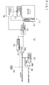
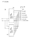
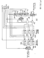
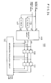
- a digital video camera 10 includes a CCD imager 12.
- the CCD imager 12 includes the number M of photo-diodes 14 for photo-electric conversion, and a plurality of vertical transfer CCDs 16, and a horizontal transfer CCD 20 as shown in Figure 2.
- Each of the vertical transfer CCDs 16 is driven by a vertical drive circuit 18, and the horizontal transfer CCD 20 is driven by a horizontal drive circuit 22.
- a drain 24 is provided in parallel to the horizontal transfer CCD 20. The drain 24 is utilized for sweeping-out unnecessary charges in a high-speed mode, e.g. quadruplication mode. That is, the unnecessary charges applied from the vertical transfer CCDs 16 through sweeping-out control gates 26 are swept-out from the drain 24.
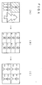
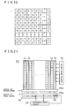
- the CCD imager 12 is provided with a mosaic-type color filter of complementary colors as shown in Figure 18(a).
- the charges of two pixels adjacent to each other in a vertical direction are mixed as shown in Figure 18(b) at an odd field or as shown in Figure 18(c) at an even field when the charges are outputted from the photo-diodes 14 to the vertical transfer CCDs 16. Accordingly, though the number of pixels of the CCD imager 12 in the vertical direction is "480", the number of lines included in a camera signal actually outputted from the CCD imager 12 with each field becomes "240".
- a method for generating a video signal from the camera signal shown in Figure 18(c) and Figure 18(d) is described in Japanese Patent Application laying-open No. 6-46431, for example, a duplicate description will be omitted here.
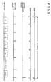
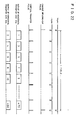
- the charge reading-out pulse is supplied to the vertical transfer CCDs 16 at every quarter field as shown in Figure 5. Furthermore, each of the vertical transfer CCDs 16 is driven by the vertical transfer pulse which has one rising edge at a half line and is generated 120 times during a sweeping-out period at every quarter field. Accordingly, the charges equal to one line are transferred to the horizontal transfer CCD 20 at every half line. That is, since the horizontal transfer CCD 20 is driven by the horizontal transfer clock which is the same as the horizontal transfer clock used in the normal mode, the charges of a succeeding line are started to be transferred from the vertical transfer CCDs 16 at a timing that the horizontal transfer CCD 20 has finished the transfer of first half charges but the second half charges are still remaining. On the other hand, a sweeping-out pulse is provided at that timing, and the sweeping-out control gates 26 are opened by the sweeping-out pulse. Accordingly, the second half charges are swept-out from the drain 24 through the sweeping-out control gates 26.
- the color camera signals corresponding to the areas A1 and A2 are alternately written into the memories a1 and a2 at every half line in a first quarter field in response to write enable signals We-a1 and We-a2 as shown in Figure 7.
- the color camera signals corresponding to the areas B1 and B2 are alternately written into the memories b1 and b2 at every half line in the second quarter field in response to write enable signals We-b1 and We-b2.
- the color camera signals corresponding to the areas C1, C2, D1 and D2 are succeedingly written into the memories c1, c2, d1 and d2 in response to write enable signals We-c1, We-c2, We-d1 and We-d2 in the same manner.
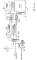
- the selection circuits 58 and 60 are controlled by a signal HSET shown in Figure 12 or Figure 13, and selectively outputs the input data or the doubled data of the input data.
- the signal HSET is a signal which becomes a low level at beginning two odd number pixels and beginning two even number pixels in each line included in the front end OB level detection area or the back end OB level detection area as shown in Figure 12 or Figure 13.
- the selection circuit 62 is controlled by a signal ODD/EVEN, and outputs the output of the selection circuit 58 at a time that the signal ODD/EVEN is a high level, and outputs the output of the selection circuit 60 at a time that the signal ODD/EVEN is a low level.
- the signal ODD/EVEN is a signal which becomes the high level at odd number pixels or the low level at even number pixels as shown in Figure 12 or Figure 13.
- an output of the odd number register 70 and an output of the even number register 72 are applied to the selection circuit 74.
- the selection circuit 74 is controlled by the signal ODD/EVEN in the same manner as that of the above selection circuit 62, and outputs the output of the odd number register 70 at a time that the signal ODD/EVEN is the high level, and outputs the output of the even number register 72 at a time that the signal ODD/EVEN is the low level.
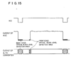
- the back end clamp timing circuit 80 is also constituted by gate circuits, ROM decoder and etc., outputs the timing signals shown in Figure 12 only at the first predetermined period, that is, a period equal to eight odd number pixels and eight even number pixels at every one line within the back end OB level detection area.
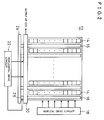
- the outputs of the first channel and the second channel thus obtained are inputted to signal processing circuits 30a and 30b as shown in Figure 23, respectively.
- Each of the signal processing circuits 30a and 30b has the same structure as that of the signal processing circuit 30 shown in Figure 9, and therefore, the outputs of the first channel and the second channel are individually clamped by the same operation.
Landscapes
- Engineering & Computer Science (AREA)
- Multimedia (AREA)
- Signal Processing (AREA)
- Physics & Mathematics (AREA)
- Spectroscopy & Molecular Physics (AREA)
- Transforming Light Signals Into Electric Signals (AREA)
- Studio Devices (AREA)
- Picture Signal Circuits (AREA)
Applications Claiming Priority (2)
| Application Number | Priority Date | Filing Date | Title |
|---|---|---|---|
| JP3647/96 | 1996-01-12 | ||
| JP8003647A JPH09200605A (ja) | 1996-01-12 | 1996-01-12 | ディジタルビデオカメラ |
Publications (2)
| Publication Number | Publication Date |
|---|---|
| EP0784397A2 true EP0784397A2 (de) | 1997-07-16 |
| EP0784397A3 EP0784397A3 (de) | 1999-01-20 |
Family
ID=11563281
Family Applications (1)
| Application Number | Title | Priority Date | Filing Date |
|---|---|---|---|
| EP97100350A Withdrawn EP0784397A3 (de) | 1996-01-12 | 1997-01-10 | Digital-Videokamera mit Hochgeschwindigkeitsmodus |
Country Status (4)
| Country | Link |
|---|---|
| US (1) | US6304292B1 (de) |
| EP (1) | EP0784397A3 (de) |
| JP (1) | JPH09200605A (de) |
| KR (1) | KR100414322B1 (de) |
Cited By (3)
| Publication number | Priority date | Publication date | Assignee | Title |
|---|---|---|---|---|
| EP0926900A3 (de) * | 1997-12-26 | 2000-06-28 | Canon Kabushiki Kaisha | Farbbildaufnahmegerät |
| EP1079602A3 (de) * | 1999-08-19 | 2004-07-07 | Canon Kabushiki Kaisha | Bildeingabevorrichtung |
| EP1594307A3 (de) * | 2004-05-07 | 2006-03-22 | Nikon Corporation | Klemmpegeleinstellvorrichtung, elektronische Kamera, Bildbearbeitungs-Vorrichtung und -Programm |
Families Citing this family (31)
| Publication number | Priority date | Publication date | Assignee | Title |
|---|---|---|---|---|
| US6747695B1 (en) * | 1997-12-05 | 2004-06-08 | Intel Corporation | Integrated CMOS imager |
| JP3172491B2 (ja) * | 1998-05-29 | 2001-06-04 | 三洋電機株式会社 | ディジタルカメラ |
| US6750910B1 (en) * | 1998-07-15 | 2004-06-15 | Texas Instruments Incorporated | Optical black and offset correction in CCD signal processing |
| JP2000106678A (ja) | 1998-09-28 | 2000-04-11 | Victor Co Of Japan Ltd | 撮像装置 |
| JP3761725B2 (ja) * | 1998-10-02 | 2006-03-29 | 株式会社リコー | 画像読取装置 |
| JP2000156822A (ja) * | 1998-11-19 | 2000-06-06 | Sony Corp | クランプ回路 |
| US6721005B1 (en) * | 1998-12-03 | 2004-04-13 | Sony Corporation | Solid state image sensor having different structures for effective pixel area and optical black area |
| US6829007B1 (en) * | 1999-09-03 | 2004-12-07 | Texas Instruments Incorporated | Digital scheme for noise filtering of optical black and offset correction in CCD signal processing |
| JP4450941B2 (ja) * | 2000-04-12 | 2010-04-14 | 富士通マイクロエレクトロニクス株式会社 | 固体撮像素子、画像処理装置及び画像処理方法 |
| US7317480B1 (en) * | 2000-10-30 | 2008-01-08 | Micron Technology, Inc. | Imaging apparatus providing black level compensation of a successive approximation A/D converter |
| JP3808349B2 (ja) * | 2001-01-12 | 2006-08-09 | 三菱電機株式会社 | 黒レベル補正装置 |
| US7586526B2 (en) * | 2001-03-29 | 2009-09-08 | Canon Kabushiki Kaisha | Image sensing apparatus with at least two transfer speeds and its control method |
| US7218351B2 (en) * | 2002-04-05 | 2007-05-15 | Victor Company Of Japan, Limited | Image-sensing apparatus for compensating video signal of a plurality of channels |
| JP3963449B2 (ja) * | 2002-10-31 | 2007-08-22 | キヤノン株式会社 | 撮像装置 |
| US7453506B2 (en) * | 2003-08-25 | 2008-11-18 | Fujifilm Corporation | Digital camera having a specified portion preview section |
| JP2007028339A (ja) * | 2005-07-19 | 2007-02-01 | Canon Inc | 撮像装置及びその制御方法及びプログラム及び記憶媒体 |
| JP4773179B2 (ja) * | 2005-10-14 | 2011-09-14 | 富士フイルム株式会社 | 撮像装置 |
| JP4554504B2 (ja) * | 2005-12-16 | 2010-09-29 | 富士通セミコンダクター株式会社 | 画像データ処理回路および画像データ処理方法 |
| JP4827524B2 (ja) * | 2005-12-26 | 2011-11-30 | キヤノン株式会社 | 撮像装置 |
| US7545418B2 (en) * | 2006-07-17 | 2009-06-09 | Jeffery Steven Beck | Image sensor device having improved noise suppression capability and a method for supressing noise in an image sensor device |
| WO2008032517A1 (fr) * | 2006-09-14 | 2008-03-20 | Mitsubishi Electric Corporation | Dispositif et procédé de traitement d'image et dispositif et procédé de capture d'image |
| US7817197B2 (en) * | 2006-09-21 | 2010-10-19 | Mediatek Singapore Pte Ltd | Optical black calibration |
| JP2008172493A (ja) * | 2007-01-11 | 2008-07-24 | Matsushita Electric Ind Co Ltd | フロントエンド信号処理方法およびフロントエンド信号処理装置 |
| JP4942493B2 (ja) * | 2007-01-24 | 2012-05-30 | 富士フイルム株式会社 | 撮像方法および装置 |
| KR101379256B1 (ko) * | 2007-07-09 | 2014-04-02 | 삼성전자주식회사 | 노이즈에 의한 신호 왜곡 보상 장치 및 그 방법 |
| JP5106017B2 (ja) * | 2007-09-20 | 2012-12-26 | 三洋電機株式会社 | カメラ |
| US20090109305A1 (en) * | 2007-10-31 | 2009-04-30 | Tiejun Dai | One-step black level calibration for image sensors |
| JP5534997B2 (ja) * | 2010-08-03 | 2014-07-02 | 富士フイルム株式会社 | 電子内視鏡システム |
| JP6110689B2 (ja) * | 2013-02-28 | 2017-04-05 | キヤノン株式会社 | 撮像装置、その制御方法及びプログラム |
| JP2015032842A (ja) * | 2013-07-31 | 2015-02-16 | ソニー株式会社 | 固体撮像素子、撮像装置、および補正方法 |
| WO2016035450A1 (ja) * | 2014-09-01 | 2016-03-10 | 株式会社島津製作所 | イメージング装置 |
Family Cites Families (13)
| Publication number | Priority date | Publication date | Assignee | Title |
|---|---|---|---|---|
| JPS5856458U (ja) * | 1981-10-09 | 1983-04-16 | 株式会社日立製作所 | カラ−固体撮像装置 |
| US4740828A (en) * | 1983-12-24 | 1988-04-26 | Canon Kabushiki Kaisha | Image sensing apparatus having a low-resolution monitor, means for reducing the amount of information in an image signal, and switching means for reducing power consumption in various operating modes |
| JPS6153766A (ja) * | 1984-08-24 | 1986-03-17 | Hitachi Ltd | インタ−ライン型電荷転送撮像素子 |
| US4856033A (en) * | 1987-03-06 | 1989-08-08 | Sony Corporation | Solid state imager device with exposure control with noise reduction |
| DE3887547T2 (de) * | 1987-03-20 | 1994-08-25 | Canon Kk | Abbildungsgerät. |
| US5172234A (en) * | 1987-08-04 | 1992-12-15 | Canon Kabushiki Kaisha | Camera having an electronic zooming display feature |
| JP2539682B2 (ja) | 1989-04-04 | 1996-10-02 | シャープ株式会社 | 電子的に拡大撮影可能な撮像装置 |
| US5040071A (en) * | 1990-03-21 | 1991-08-13 | Eastman Kodak Company | Image sensor having multiple horizontal shift registers |
| KR0108917Y1 (en) * | 1991-12-05 | 1997-11-08 | Samsung Electronics Co Ltd | Digital clamping circuit |
| JP3143193B2 (ja) | 1992-02-28 | 2001-03-07 | 三洋電機株式会社 | ディジタルカメラ信号処理回路 |
| JP3264698B2 (ja) * | 1992-06-30 | 2002-03-11 | キヤノン株式会社 | 撮像装置 |
| JP3022130B2 (ja) | 1993-01-28 | 2000-03-15 | 三洋電機株式会社 | 高速撮影装置 |
| JP3241882B2 (ja) | 1993-07-08 | 2001-12-25 | ソニー株式会社 | 固体撮像装置 |
-
1996
- 1996-01-12 JP JP8003647A patent/JPH09200605A/ja active Pending
-
1997
- 1997-01-09 US US08/780,930 patent/US6304292B1/en not_active Expired - Lifetime
- 1997-01-10 EP EP97100350A patent/EP0784397A3/de not_active Withdrawn
- 1997-01-11 KR KR1019970000585A patent/KR100414322B1/ko not_active Expired - Fee Related
Cited By (7)
| Publication number | Priority date | Publication date | Assignee | Title |
|---|---|---|---|---|
| EP0926900A3 (de) * | 1997-12-26 | 2000-06-28 | Canon Kabushiki Kaisha | Farbbildaufnahmegerät |
| US7142233B1 (en) | 1997-12-26 | 2006-11-28 | Canon Kabushiki Kaishi | Image pickup element |
| EP1079602A3 (de) * | 1999-08-19 | 2004-07-07 | Canon Kabushiki Kaisha | Bildeingabevorrichtung |
| US7053941B1 (en) | 1999-08-19 | 2006-05-30 | Canon Kabushiki Kaisha | Image input apparatus |
| US7542081B2 (en) | 1999-08-19 | 2009-06-02 | Canon Kabushiki Kaisha | Image input apparatus |
| EP1594307A3 (de) * | 2004-05-07 | 2006-03-22 | Nikon Corporation | Klemmpegeleinstellvorrichtung, elektronische Kamera, Bildbearbeitungs-Vorrichtung und -Programm |
| US7688356B2 (en) | 2004-05-07 | 2010-03-30 | Nikon Corporation | Clamp level adjusting apparatus, electronic camera, image processing apparatus, and image processing program |
Also Published As
| Publication number | Publication date |
|---|---|
| US6304292B1 (en) | 2001-10-16 |
| KR970060873A (ko) | 1997-08-12 |
| KR100414322B1 (ko) | 2004-03-31 |
| EP0784397A3 (de) | 1999-01-20 |
| JPH09200605A (ja) | 1997-07-31 |
Similar Documents
| Publication | Publication Date | Title |
|---|---|---|
| EP0784397A2 (de) | Digital-Videokamera mit Hochgeschwindigkeitsmodus | |
| US6157407A (en) | Digital camera with analog and digital clamp circuit | |
| EP0630151B1 (de) | Ansteuermethode für einen Festkörperbildaufnehmer | |
| US5734424A (en) | Image pickup apparatus capable of providing moving video signal and still video signal | |
| US4992860A (en) | Color scanning system | |
| US7408587B2 (en) | Image conversion device, image conversion method and data conversion circuit as well as digital camera | |
| US6519000B1 (en) | Image pickup apparatus with mode switching between a still picture mode and a moving picture mode | |
| CA1269446A (en) | Image sensing apparatus | |
| EP0109261B1 (de) | Farbfernsehkamera | |
| EP0569202B1 (de) | Festkörperbildaufnahmevorrichtung mit elektronischem Verschluss | |
| US20040080652A1 (en) | Electric camera | |
| US6587149B1 (en) | Video camera with progressive scanning and dynamic range enlarging modes | |
| CN104170376A (zh) | 图像处理设备、成像装置、图像处理方法及程序 | |
| US5043817A (en) | Image pick-up apparatus with electronic zooming-in | |
| US4528595A (en) | Line transfer imager and television camera including such an imager | |
| JPH09200617A (ja) | 撮像装置 | |
| JP2001245213A (ja) | 撮像装置 | |
| US5150204A (en) | Solid state image pickup having plural pixels arranged on plural lines | |
| US5191409A (en) | Color scanning system | |
| US6339213B2 (en) | Solid state imaging device and method for driving the same | |
| US20040130642A1 (en) | Solid-state image pickup device, drive method therefor and camera | |
| JPH06205307A (ja) | 固体撮像素子及び加算装置 | |
| JP2004215249A (ja) | 固体撮像装置及びその駆動方法、並びにカメラ | |
| JP2897665B2 (ja) | 固体撮像素子の駆動方法 | |
| US5150388A (en) | Solid state image sensing device output |
Legal Events
| Date | Code | Title | Description |
|---|---|---|---|
| PUAI | Public reference made under article 153(3) epc to a published international application that has entered the european phase |
Free format text: ORIGINAL CODE: 0009012 |
|
| AK | Designated contracting states |
Kind code of ref document: A2 Designated state(s): DE FR GB |
|
| PUAL | Search report despatched |
Free format text: ORIGINAL CODE: 0009013 |
|
| AK | Designated contracting states |
Kind code of ref document: A3 Designated state(s): DE FR GB |
|
| 17P | Request for examination filed |
Effective date: 19990707 |
|
| 17Q | First examination report despatched |
Effective date: 20031203 |
|
| GRAP | Despatch of communication of intention to grant a patent |
Free format text: ORIGINAL CODE: EPIDOSNIGR1 |
|
| STAA | Information on the status of an ep patent application or granted ep patent |
Free format text: STATUS: THE APPLICATION HAS BEEN WITHDRAWN |
|
| 18W | Application withdrawn |
Effective date: 20051107 |