EP0109261B1 - Farbfernsehkamera - Google Patents
Farbfernsehkamera Download PDFInfo
- Publication number
- EP0109261B1 EP0109261B1 EP83306839A EP83306839A EP0109261B1 EP 0109261 B1 EP0109261 B1 EP 0109261B1 EP 83306839 A EP83306839 A EP 83306839A EP 83306839 A EP83306839 A EP 83306839A EP 0109261 B1 EP0109261 B1 EP 0109261B1
- Authority
- EP
- European Patent Office
- Prior art keywords
- digital
- picture
- signal
- circuit
- pixel
- Prior art date
- Legal status (The legal status is an assumption and is not a legal conclusion. Google has not performed a legal analysis and makes no representation as to the accuracy of the status listed.)
- Expired
Links
- 230000001360 synchronised effect Effects 0.000 claims description 60
- 238000012545 processing Methods 0.000 claims description 52
- 238000001514 detection method Methods 0.000 claims description 27
- 238000012937 correction Methods 0.000 claims description 23
- 238000006243 chemical reaction Methods 0.000 claims description 22
- 230000003111 delayed effect Effects 0.000 claims description 7
- 230000003287 optical effect Effects 0.000 claims description 4
- 238000012935 Averaging Methods 0.000 claims 2
- 239000003086 colorant Substances 0.000 claims 2
- 230000008054 signal transmission Effects 0.000 claims 2
- 238000000034 method Methods 0.000 description 26
- 230000006870 function Effects 0.000 description 9
- 238000012546 transfer Methods 0.000 description 4
- 238000004519 manufacturing process Methods 0.000 description 3
- 238000007796 conventional method Methods 0.000 description 2
- 238000011161 development Methods 0.000 description 2
- 238000010586 diagram Methods 0.000 description 2
- 239000003990 capacitor Substances 0.000 description 1
- 238000013461 design Methods 0.000 description 1
- 230000000694 effects Effects 0.000 description 1
- 238000011156 evaluation Methods 0.000 description 1
- 238000012986 modification Methods 0.000 description 1
- 230000004048 modification Effects 0.000 description 1
- 230000035945 sensitivity Effects 0.000 description 1
Images


Classifications
-
- H—ELECTRICITY
- H04—ELECTRIC COMMUNICATION TECHNIQUE
- H04N—PICTORIAL COMMUNICATION, e.g. TELEVISION
- H04N23/00—Cameras or camera modules comprising electronic image sensors; Control thereof
- H04N23/80—Camera processing pipelines; Components thereof
- H04N23/84—Camera processing pipelines; Components thereof for processing colour signals
-
- H—ELECTRICITY
- H04—ELECTRIC COMMUNICATION TECHNIQUE
- H04N—PICTORIAL COMMUNICATION, e.g. TELEVISION
- H04N25/00—Circuitry of solid-state image sensors [SSIS]; Control thereof
- H04N25/10—Circuitry of solid-state image sensors [SSIS]; Control thereof for transforming different wavelengths into image signals
- H04N25/11—Arrangement of colour filter arrays [CFA]; Filter mosaics
- H04N25/13—Arrangement of colour filter arrays [CFA]; Filter mosaics characterised by the spectral characteristics of the filter elements
- H04N25/135—Arrangement of colour filter arrays [CFA]; Filter mosaics characterised by the spectral characteristics of the filter elements based on four or more different wavelength filter elements
- H04N25/136—Arrangement of colour filter arrays [CFA]; Filter mosaics characterised by the spectral characteristics of the filter elements based on four or more different wavelength filter elements using complementary colours
Definitions
- This invention relates to a color camera that is used in the field of TV-studio camera system, consumer VTR-camera system, surveilance camera system and an object-detection camera system.
- the conventional method to realize signal process parts of the color camera is mainly based on analog signal processing, so that the color camera using this conventional technique has the following disadvantages:
- a camera having image sensing means for detecting an image, the image sensing means receiving optical signals to produce two alternately different picture-pixel signals - a first picture-pixel signal and a second picture-pixel signal, the first picture-pixel signal being composed of repeated combination of two different color pixel informations which are shifted out with a repetition frequency of f c in a horizontal synchronous interval of television signal, and the second picture-pixel signal being composed of repeated combination of the next two different color pixel informations which are different from the two different color pixel informations in the first picture-pixel signal and are shifted out with a repetition frequency of f c in the next coming horizontal synchronous interval of the television signal.
- Such an image sensing means lends itself to use with digital processing circuitry since the pixels are provided as discrete pulses.
- the present invention provides analog to digital converting means for receiving said two alternately different picture-pixel signals to produce two alternate digital picture-pixel signals; digital chrominance signal processing means for receiving said two alternate digital picture-pixel signals to produce two independent digital chrominance-difference signals; digital luminance signal processing means for receiving said two alternate digital picture-pixel signals to produce digital luminance signal; color television signal encoding means for receiving said two independent digital chrominance-difference signals and said digital luminance signal to produce color television signal; control circuit means for generating first, second, third, fourth timing pulses, said timing pulses respectively controlling said A/D converting means, said digital chrominance signal processing means, said digital luminance signal processing means and said color television signal encoding means; and driving means for driving said image sensing means, said color television signal encoding means and said control circuit means.
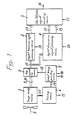
- Fig. 1 is a basic block diagram of a color camera system, showing a configuration of this invention, in which: an image sensing means 1 is connected to an A/D converting means 2; the A/D converting means 2 is connected to a digital chrominance signal processing means 4 and a digital luminance signal processing means 3; the digital chrominance signal processing means 4 and the digital luminance signal processing means 3 are connected to a color television signal encoding means 5; and a driving means 6 is coupled to the image sensing means 1 and a control timing generating means 7.
- the image sensing means With receiving optical image signals, the image sensing means produces two alternately different kind of picture-pixel signals - a first picture-pixel signal 9 and a second picture-pixel signal 10.
- the first picture-pixel signal 9 is composed of repeated combination of two different color pixel informations which are shifted out at a repetition frequency of f c in a horizontal synchronous interval of a television signal.
- the second picture-pixel signal 10 is composed of repeated combination of next two different color pixel informations which are different from the two color pixel informations and are shifted out with a repetition frequency of f c on the next coming horizontal synchronous interval of the television signal.
- the above described operation of the image sensing means is controlled by control signals 11 supplied from the driving means 6.
- the picture-pixel signals 9, 10 are analog signals or analog' sampled signals.
- the picture-pixel signals 9, 10 are converted to a digital picture-pixel signal 12 by passing the A/D converting means 2.
- the digital picture-pixel signal 12 is fed to the digital chrominance signal processing means 4.
- This processing means 4 produces a set of two independent digital chrominance-difference signals 14, 15.
- the digital picture-pixel signal 12 is also fed to the digital luminance signal process means 3.
- This process means 3 produces digital luminance signal 13.
- the digital luminance signal 13 and digital chrominance signals 14, 15 are fed to the color television signal encoding means 5.
- the encoding means 5 produces a standard color television signal as an output.
- This standard television signal may be analog signal for some application like a compact color camera and may be digital signal for the other application like object-detective camera system.
- the A/D converting means 2, the digital luminance signal processing means 3, the digital chrominance signal processing means 4 and the color television encoding means 5 are respectively controlled by the first, second, third and fourth timing pulse- systems 18, 19, 20 and 21 which are generated by the control timing generating means 7 in accordance with the timing 17 of the driving means 6.
- the main signal processing means for a color camera is realized on a digital circuit system. This is one of the major advantages of this invention.
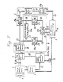
- Fig. 2 is one example of the specific configuration of the invented color camera system, in which detailed configurations for the digital chrominance signal means 4 and the digital luminance signal processing means 3 are disclosed.
- a one horizontal digital memory means 23 first digital chrominance signal detection means 24, second digital chrominance signal detection means 25, data-path multiplex means 26 and digital white balance means 22 are provided in the digital chrominance signal means 4.
- the digital picture-pixel signal 12 is converted to a digital picture-pixel signal 27 by passing the digital white balance means 22, in which said digital picture-pixel signal 27 is a white balanced signal.
- the digital picture-pixel signal 27 is converted to a digital picture-pixel signal 28 by passing the one horizontal digital memory means 23, in which the digital picture-pixel signal 28 is delayed by a period of one horizontal synchronous interval. Therefore, in one horizontal synchronous interval, when the digital picture-pixel signal 27 is composed of the information of the picture-pixel signal 9, the digital picture-pixel signal 28 is composed of the information of the picture-pixel signal 10. In the next horizontal synchronous interval, the relations are reversed, that is, the digital picture-pixel signal 27 is composed of the information of the picture-pixel signal 10 and the digital picture-pixel signal 28 is composed of the information of the picture-pixel signal 9.
- two different type of digital picture-pixel signals 27, 28 are fundamental signals to produce first and second independent digital chrominance-difference signals 14, 15.
- a first digital chrominance signal detection means 24 the digital picture-pixel signal 27 is converted to a digital chrominance-difference signal 29, in which the information of the picture-pixel signal 9 and the picture-pixel signal 10 are rotated alternately in accordance with the repetition rate of horizontal synchronous interval.
- the digital picture-pixel signal 28 is converted to a digital chrominance-difference signal 30, in which the information of the picture-pixel signal 9 and the picture-pixel signal 10 are also rotated alternately in accordance with the repetition rate of horizontal synchronous interval.
- the digital chrominance-difference signal 30 is a delayed signal over the digital chrominance-difference signal 29 by a period of one horizontal synchronous interval.
- data-path multiple means 26 produces first and second independent digital chrominance-difference signals 14, 15, in which the digital chrominance-difference signal 14 is composed of the information of the first picture-pixel signal 9 in each coming horizontal synchronous interval and the digital chrominance-difference signal 15 is composed of the information of the second picture-pixel signal 10 in each coming horizontal synchronous interval.
- the relation of the digital chrominance-difference signals 14, 15 vs. the information of first and second picture-pixel signals 9, 10. may be exchanged from the above defined relation.
- the digital chrominance signal processing means 3 comprises a one horizontal digital memory means 23, first and second digital chrominance signal detection means 24, 25 and a data-path multiplex means 26.
- a digital luminance process circuit 31, a digital-gamma correction circuit 32 and a digital delay-circuit 33 are provided in the digital luminance signal processing means 3.
- the digital picture- .pixel signal 27 is converted to a basic-digital luminance signal 34 by passing the digital luminance process circuit 31.
- the basic-digital luminance signal 34 is converted to a delayed basic-digital luminance signal 35 by passing the digital delay-circuit 33.
- the delayed basic-digital luminance signal 35 is then converted to a digital luminance signal 13 by passing the digital-gamma correction circuits 32, in which the digital luminance signal 13 is a gamma corrected digital luminance signal over the basic-digital luminance signals 35, 34.
- the delay circuit 33 It is the task of the delay circuit 33 to cancel out a relative output-timing difference between the digital chrominance-difference signals 14, 15 and the digital luminance signal 13. This sort of difference will depend on design-configurations of the digital chrominance signal processing means 4 and digital luminance signal processing means 3. So, in some case, the function of the digital delay circuit 33 may be provided in the digital chrominance signal processing means 4.
- the basic circuit for the digital luminance signal processing means 3 comprises digital luminance signal process circuit 31 and digital-gamma correction circuit 32. Moreover, it is not impossible to take out the digital-gamma correction circuit 32 from the digital luminance signal processing means 3, if the gamma-corrected picture-pixel signal is supplied at the input end of the A/D converting means 2.
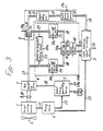
- Fig. 3 is another example of the specific configuration of the invented color camera system, in which another detailed configuration for the digital chrominance signal processing means 4 is disclosed. Therefore, in Fig. 3 the configuration of the invented color camera system is basically same as the configuration shown in Fig. 2 except the configuration for the digital chrominance signal processing means 4.
- a one horizontal digital memory means 23 First digital chrominance signal detection means 24, second digital chrominance signal detection means 25, data-path multiplex means 26 and digital white balance means 40 are provided in the digital chrominance signal processing means 4.
- the digital white balance means 40 is placed at the output end of the data-path-multiplex means 26.
- digital picture-pixel signal 37, digital chrominance-difference signal 38, digital chrominance-difference signal 39, digital chrominance-difference signal 42 and digital chrominance-difference signal 43 are respectively same as the digital picture-pixel signal 28, the digital chrominance-difference signal 29, the digital chrominance-difference signals 30, the digital chrominance-difference signal 14 and the digital chrominance-difference signal 15 except that those signals 37, 38, 39, 42 and 43 are not white balanced signals.
- the data-path multiplex means 26 produces the digital chrominance-difference signals 42, 43, in which the digital chrominance-difference signal 42 is composed of the information of the first picture-pixel signal 9 in each horizontal synchronous interval and the digital chrominance-difference signal 43 is composed of the information of the second picture-pixel signal 10 in
- the digital chrominance-difference signal 42 and the digital chrominance-difference signal 43 are respectively converted to the chrominance-difference signal 14 and the chrominance-difference signal 15 by passing the digital white balance means 40.
- Fig. 4 is one example of the image sensing means 1, in which a combination of magenta (M), green (G), cyan (C) and yellow (Y) color filters are placed on MOS structured photodiodes which make an array of picture-pixel elements 44-47.
- the array is simplified one. Actually the array is consisted of several hundred of picture-pixel elements in both horizontal and vertical directions.
- H charge coupled device
- these groups of M picture-pixel signals and G picture-pixel signals are respectively swept out through a terminal 84 and a terminal 85 during the period of the horizontal synchronous interval H, at a repetition rate of 1/f c .
- the C picture-pixel signals generated underneath the elements 50, 52, 54 are simultaneously transferred into the CCD shift register 82, and the Y picture-pixel signal generated underneath the elements 51, 53, 55 are also simultaneously transferred into the CCD shift register 83.
- a couple of repetitions of this one field interval scanning make a content of one frame interval scanning for TV signals.
- an interlaced scanning is performed by changing selection way of picture-pixel elements along the row lines on the image sensing means 1.
- the above sort of operations on the image sensing means 1 are performed by the aid of control signals 11.
- the M and G picture-pixel signals are respectively produced through the terminals 84 and 85 during the period of horizontal synchronous interval H 1
- the C and Y picture-pixel signals are respectively produced through the terminals 84 and 85 during the period of horizontal synchronous interval H 2 .
- the above two different modes of outputs are repeated alternately, and the operation modes of the first CCD shift register 82 and the second CCE shift register 83 are maintained in reversed phase at a repetition rate of 1/f c .
- the image sensing means 1 produces a stream of first kind of picture-pixel signal 9 with information of M and G picture-pixel signals in a horizontal synchronous interval H 1 and produces a stream of second kind of picture-pixel signal 10 with information of C and Y picture-pixel signals in a next horizontal synchronous interval H 2 .
- Fig. 5 shows magnified analog-sampled waveforms of the first kind of picture-pixel signal 9 and second kind of picture-pixel signal 10 generated by the image sensing means 1, and also shows digital picture-pixel signals 12A, 12B which are converted signals from the picture-pixel signals 9, 10 by the aid of the A/D converting means 2. Timing pulses for operating the A/D converting means 2 are also shown in Fig. 5.
- the image sensing means 1 produces two kinds of picture-pixel signals through the terminals 84, 85 in a horizontal synchronous interval H 1 or H z . So, it is necessary to mix-up the two kinds of picture-pixel signals into a stream of picture-pixel signals.
- an analog to digital (A/D) conversion circuit 96 and an analog switch circuit 95 are provided in the A/D converting means 2.
- the image sensing means 1 produces the first picture-pixel signal 9 having a stream of M picture-pixel signals 86a-86e through the terminal 84 and having a stream of G picture-pixel signals 87a-87e through the terminal 85.
- the analog switch circuit 95 selects the stream of M picture-pixel signals 86a-86e as input signals for the A/D conversion circuit 96.
- the A/D conversion circuit 96 converts the stream of M picture-pixel signals into digital M picture-pixel signals 101a-101e by receiving a stream of conversion pulses 90 through the terminal 97.
- the analog switch circuit 95 selects a stream of G picture-pixel signals 87a-87e as input signals for the A/D conversion circuit 96.
- the A/D conversion circuit 96 converts the stream of G picture-pixel signals 87a-87e into G picture-pixel signals 102a-102e by receiving the stream of conversion pulses 90 through the terminal 97.
- the analog switch circuit 95 mixes-up two streams of picture-pixel signals M and G in this case, at a repetition rate of 2/f c and at the almost same time the A/D conversion circuit 96 is operated with a repetition rate of 1/f c synchronized by the rate of 2/f c . Therefore, analog informations of M and G picture-pixel signals 86a-86e, 87a-87e are converted and produced as a stream of digital picture-pixel signals 12a through the terminal 100a.
- the image sensing means 1 produces second kind of picture-pixel signals 10 having a stream of C picture-pixel signals 88a-88e through the terminal 84 and having a stream of Y picture-pixel signals 89a89e through the terminal 85.
- analog switch circuit 95 and the A/D conversion circuit 96 it is apparent that analog informations of C and Y picture-pixel signals 88a-88e, 89a89e are converted and produced as a stream of digital picture-pixel signals 12b through the terminal100a.
- the A/D converting means 2 comprises the analog switch circuit 95 and the A/D conversion circuit 96, in which the first timing pulse system 18 shown in Figs. 1, 2 and 3 correspond to the stream of conversion pulses 90.
- Fig. 6(b) shows another example of the A/D converting means 2, in which: a first A/D conversion circuit 104 coupled to the image sensing means 1 through the terminal 84 for receiving first or second kind of picture-pixel signals 9, 10 produces digital information of the picture-pixel signal 9, 10; a second A/D conversion circuit 105 coupled to image sensing means 1 through the terminal 85 for receiving first or second kind of picture-pixel signals 9, 10 produces also digital information of the picture-pixel signals 9, 10; a first digital latch circuit 106 coupled to the first A/D conversion circuit 104 receives the digital informations, a second digital latch circuit 107 coupled to the second A/D conversion circuit 105 receives also the digital informations.
- Outputs of the first and second latch circuits 106, 107 are coupled in common, respectively, and operating timings for the first AID conversion circuit 104 and the first latch circuit 106 and for the second A/D conversion circuit 105 and the second latch circuit 107 are alternately phase shifted to produce digital picture-pixel signals 12a, 12b.
- the detailed operations of the above configuration on the A/D converting means 2 will be described below for the purpose to clarify the features of this invention.
- the image sensing means 1 produces the first kind of analog picture-pixel signal 9
- the M picture-pixel signals 86a-86e are generated through the terminal 84 and the G picture-pixel signals 87a-87e are generated through the terminal 85.
- the first A/D conversion circuit 104 converts the stream of M picture-pixel signals 86a-86e into a stream of digital picture-pixel signals 101a-101e.
- the stream of digital picture-pixel signals 101a-101e are latched up by the first latch circuit 106 with getting small amount of delay time td in each of the timing intervals 98a-98e and are produced as output signals through the common terminal 100b.
- the second A/D conversion circuit 105 converts the stream of G picture-pixel signals 87a-87e into a stream of digital picture-pixel signals 102a-102e.
- the stream of the digital picture-pixel sighals 102a-102e are latched up by the second latch circuit 107 with getting small amount of delay time td in each of the timing intervals 99a-99e and are produced as output signals through the common terminal 100b.
- output terminals of the first latch circuits 106 are maintained open conditions.
- the first digital latch circuit 106 and the second digital circuit 107 are operated alternately at a repetition rate of 1/(2f c ) and output terminals of these latches 106, 107 are respectively connected in common. Therefore, these operating conditions make it possible to mix-up two streams of M picture-pixel signals 86a-86e and G picture-pixel signal 87a-87e and to convert into digital picture-pixel signal 12a produced through the common terminal 100b.
- the image sensing means produces the second kind of analog picture-pixel signal 10 having the C picture-pixel signals 88a-88e-and the Y picture-pixel signals 89a-89e.
- the image sensing means produces the second kind of analog picture-pixel signal 10 having the C picture-pixel signals 88a-88e-and the Y picture-pixel signals 89a-89e.
- the A/D converting means 2 comprises the first and second A/D conversion circuits 104, 105 and the first and second digital latch circuits 106, 107, in which the first timing pulse system 18 shown in Figs. 1, and 3 correspond to the stream of pulses 91 and 92.
- Fig. 7 shows a configuration of the digital chrominance signal detection means 24, 25.
- Fig. 8 shows an example of the digital chrominance detection circuit.
- Fig. 9 shows relations of timing pulses, input digital picture-pixel signals, digital picture-pixel signal on process and output of digital chrominance difference signals generated on the digital chrominance detection circuit. The detailed operation of the digital chrominance detection means will be described below for the purpose to clarify the features of this invention.
- a pixture-pixel shift circuit 110, a picture pixel inverting circuit 111 and a digital addition circuit 112 are provided in the digital chrominance detection means 24, 25.
- the picture-pixel shift circuit 110 produces a unshifted digital picture-pixel signal 113 and a shifted digital picture-pixel signal 114 for a period of 1/f c .
- the shifted digital picture-pixel signal 114 is inverted to a digital picture-pixel signal 115 by the picture-pixel inverting circuit 111.
- the unshifted digital picture-pixel signal 113 and the shifted and inverted digital picture-pixel signal 115 are added for producing a digital chrominance difference signal 116 by the digital addition circuit 112.
- the image sensing means 1 with a set of M, G, C, Y color informations are chosen as an example, it is the task of this digital chrominance detection means 24, 25 for receiving a stream of M, G, M, G or C, Y, C, Y digital picture-pixel signals 12, 27, 28 or 37 as inputs to produce a stream of M-G, M ⁇ G,... or C-Y, C-Y, ... digital chrominance difference signals 29, 30, 38 or 39.
- the digital picture-pixel shift circuit 110 selectively detects a stream of G digital picture-pixel signals and shifts these by a period of 1/f e .
- the shifted G digital picture-pixel signals are inverted to -G digital picture-pixel signals.
- the digital addition circuit 112 With receiving the stream of unshifted M digital picture-pixels and the stream of-G digital picture-pixel signals, the digital addition circuit 112 produces a stream of M-G, M-G,... digital chrominance difference signals. In the same manner, a stream of C-Y, C-Y, ... digital chrominance difference signals are also produced.
- a first digital latch circuit 117, a second digital latch circuit 118, a third digital latch circuit 119 and D-flip-flop (D-FF) circuits 120 are provided in the digital picture-pixel shift circuit 110.
- a digital inverting circuit 121 is provided in the picture-pixel inverting circuit 111.
- the digital picture-pixel signals 12, 27, 28 or 38 are latched up by the first digital latch circuit 117 at a repetition rate of 1/f c .
- the latched up outputs of the first digital latch circuit are applied to the second and third digital latch circuits 118, 119.
- the second and third digital latch circuits 118, 119 are alternately latched up at a repetition rate of 1/(2f,:).
- the timing clock pulses generated by the D-FF circuit 120 control the second and third latch circuits 118, 119.
- the outputs of the third digital latch circuits 119 are applied to the digital inverting gate circuit 121.
- the outputs of the second digital latch circuit 118 and the outputs of the digital inverting gate circuit 121 are supplied as inputs for the digital addition circuit 112.
- the detailed timing operation on the digital chrominance detection circuit shown in Fig. 8 will be described below with reference to Fig. 9.
- the first digital latch circuit 117 In a horizontal synchronous interval H i , with receiving digital picture-pixel signals 12a as inputs and with receiving a stream of pulses 123 through the terminal 122, the first digital latch circuit 117 produces a stream of M picture-pixel signals 101 and G picture-pixel signals 102 as latched up outputs. At the same time, a stream of pulses 126 and a stream of pulses 127 are respectively produced through the Q output terminal and the Q output terminal of the D-FF circuit 120. As the second digital latch circuit 118 is latched on by the stream of pulses 126 during the time interval 128a-128e, a stream of M picture-pixel signals 130 are selectively latched up at a repetition rate of 1/(2f c ).
- a stream of G picture-pixel signals 131 are selectively latched up at a repetition rate of 1/(2f e ).
- the M picture-pixel signals and G picture-pixel signals are relatively shifted by a period of one picture-pixel interval 1/f c .
- the above are basic operation of the picture-pixel shift circuit 110.
- the G picture-pixel signals 131 are inverted to the -G picture-pixel signals 132 by the -digital inverting gate circuit 121 just after the completion of the latch up of the G picture-pixel signals 131.
- the digital addition circuit 112 produces a stream of M-G digital chrominance difference signals. These signals correspond to the one of the digital chrominance difference signals 29, 30, 38 or 39.
- next horizontal synchronous interval H 2 as the digital picture-pixel signals 12b with informations of C, Y, C, Y, ... are applied to the first digital latch circuit 117 as its inputs, it is apparent that the digital addition circuit 112 produces a stream of C-Y digital chrominance difference signals by using the same operation described above on the digital picture-pixel signals 12a.
- the stream of pulses 123 supplied to the terminal 113 and horizontal synchronous pulses supplied to the terminal 113 correspond respectively to the control pulses 20b, 20c.
- the clock input terminal which controls latch up timing is designated by CK.
- Fig. 10 is an example of the one-horizontal digital memory means 23.
- Fig. 11 shows a relation of timing pulses, input and output digital picture-pixel signals.
- the detailed operations of the one horizontal digital memory means 23 will be described for the purpose to clarify the features of this invention.
- a second digital latch circuit 134 a third digital latch circuit 135, a random access memory (RAM) circuit 136, an address counter circuit 137 and a timing pulse generating circuit 144 are provided in the one horizontal digital memory means 23.
- a first and a fourth digital latch circuits 145, 146 are respectively used for an input and an output latch circuits of the one horizontal digital memory means 23.
- the first D-FF circuit 138 produces a stream of pulses 153 reset at a timing 152a through Q terminal at a repetition rate of 1/f c and also produces a stream of pulses 154 reset at the timing 152a through Q terminal at a repetition rate of 1/f e
- the second D-FF circuit 139 produces a stream of pulses 155 reset at a timing 152cthrough Q terminal at a repetition rate of 1/f e .
- NOR gates 142, 143 With receiving the stream of pulses 153 and the stream of pulses 155 respectively through the terminals 149 and 150, a combination of NOR gates 142, 143 produces a stream of pulses 157 through the terminal 156.
- the stream of pulses 157 are used for controlling write-timing of digital picture-pixel data into the RAM circuit 136.
- the reset timing 152a defined above is repeated at a rate of one horizontal synchronous interval.
- a detailed reading and writing operations of the RAM circuit 136 will be described below by using the stream of pulses 153, 154 and 157.
- a stream of pulses 153, 154, 157 are respectively reset, and at the same time the address counter circuit 137 is also reset.
- the address counter circuit 137 defines the first effective address data 159a.
- the RAM circuit 136 produces effective read-out data 161 by sensing H level logic on the stream of the pulses 157 and accepts effective write-in data 162 by sensing L level logic on the stream of the pulses 157.
- the third digital latch circuit 134 is latched up and connected to input terminals of the RAM circuit 136.
- the effective data 161 are stored into the first address of the RAM circuit 136 just before one horizontal synchronous interval are transferred into the third digital latch circuit 135 as shown by arrow 167 and holded as-effective output data 170a.
- the second digital latch circuit 134 is latched up at the same timing, and input picture-pixel data 171a stored in the first digital latch circuit 145 are shifted into the second digital latch circuit 134 as shown by arrow 172 and stored as effective input data 169a. Then, during a time interval 165, as a latch up interval 166 for the effective input data 169a and a presence interval for the effective write data 162 are overlapped, the effective input data 169a are stored into the first address of the RAM circuit 136 as shown by arrow 168. The new written-in data 162 are continuously stored into the first address until the first address is accessed again in the next coming horizontal synchronous interval.
- the address counter circuit 137 sets a second address data 159b, and at a timing 163b effective output data 170b are produced in the third digital latch circuit 135, and an effective input data 169b are stored into the second address of the RAM circuit 136.
- the RAM circuit 136 stores digital picture-pixel signals 12, 27 as effective input data and produces effective output data as digital picture-pixel signals delayed by a period of one horizontal synchronous interval.
- the first digital latch circuit 145 and the fourth digital latch circuit 146 are operated by the stream of pulses 153.
- the function of the fourth digital latch circuit 146 is identical with the function of the first digital latch circuit 117 shown in Fig. 8.
- the function of the first digital latch circuit 145 is assumed as a digital buffer latch circuit connected between the digital white balance means 22 and the one horizontal digital memory means 23.
- the function of the first digital latch circuit 145 is assumed as a digital buffer latch circuit connected between the A/D converting means and the one horizontal memory means 23.
- the timing pulse generating circuit 144 comprises the two D-FFs 138, 139 and the four NOR circuits 140-143 as shown in Fig. 10, it is apparent that the means should not be recognized as an only means for realizing the timing pulse generating circuit 144.
- the timing clock pulses with a repetition rate of 1/(2f c ) supplied through the terminal 147 and the reset timing pulses-with a repetition rate of one horizontal synchronous interval supplied through the terminal 148 correspond to the timing pulse system 20a shown in Figs. 2 and 3.
- Fig. 12 is another example of the one horizontal digital memory means 23 which is composed of parallel digital shift register with M stages x N bits sizes. Lateron, N bits is assumed to 8 bits parallel data.
- the number of the stages M is defined as:
- the clock frequency f c is chosen to be 7.2 MHz, which is two times f b , M becomes 455 bits. If the clock frequency f c is chosen to 14.4 MHz, which is four times f b , M becomes 910 bits. In this way, if f c is chosen to be integer times f b , the value of M becomes also integer number.
- the parallel 8-bit shift registors 173-180 are clocked by common clocking pulses. These clocking pulses correspond to the timing pulse system 20a.
- the purpose of the digital latch circuits 145, 146 shown in Fig. 12 are identical with the first and the fourth digital latch circuits shown in Fig. 10. As described above with reference to Fig. 12, it is apparent that the one horizontal digital memory means 23 comprises parallel shift registors with size of M stages by N bits.
- Fig. 13 is an example of the data-path multiplex means 26.
- a first digital latch circuit 181, a second digital latch circuit 182, a third digital latch circuit 183 and a fourth digital latch circuit 184 are provided in the data-path multiplex means 26, in which: inputs of the first digital latch circuit 181 and the second digital latch circuit 182 are connected in common; inputs of the third digital latch circuit 183 and the fourth digital latch circuit 184 are also connected in common; outputs of the first and third digital latch circuits 181, 183 are connected in common; outputs of the second and fourth digital latch circuits 182, 184 are also connected in common; and control gate timing for the first and fourth digital latch circuits 181, 184 are connected to be reverse phased to that for the second and third digital latch circuits 182, 183, at a repetition rate of two horizontal synchronous intervals 2H.
- Fig. 14 shows relations of the digital chrominance difference signals 29, 30, produced respectively at the outputs of the digital chrominance signal detection means 24, 25, and the digital chrominance difference signals 14, 15, produced at the outputs of the data-path multiplex means 26.
- the detailed operation of this data-path multiplex means 26 will be described below to clarify the features of this inventions.
- the relations between the digital chrominance difference signal 29 and the digital chrominance difference signal 30 are alternately phase shifted by one horizontal synchronous interval H, and both digital chrominance difference signals 29, 30 are composed of a stream of either M-G or C-Y chrominance difference signals repeated at a rate of two horizontal synchronous interval 2H. Therefore, it is the task of the data-path multiplex means 26 for receiving these uncontinuous M-G, C-Y, M-G, C-Y signals 29, 30 as inputs to produce two independent and continuous stream of M-G chrominance difference signals 14 and C-Y chrominance difference signals 15.
- the digital chrominance difference signals 29 and the digital chrominance difference signals 30 are respectively supplied to the common inputs of the first and second digital latch circuits 181, 182 and the common inputs of the third and fourth digital latch circuits 183,184. Besides, a stream of pulses 186 with a repetition rate of the 2H are supplied to a terminal 185. Then, during the horizontal synchronous interval 188a the first digital latch circuit 181 becomes to be conductive with receiving the stream of timing pulse 187 through CG terminal, and the third digital latch circuit 183 becomes to be non-conductive with receiving the stream of timing pulses 186 through CG terminal.
- informations of the digital M-G chrominance difference signals 29a are produced through the common output 189 of the first and third digital latch circuits 181, 183.
- the second latch circuit 182 becomes to be non-conductive with receiving the stream of pulses 186 through CG terminal
- the fourth digital latch circuit 184 becomes to be conductive with receiving the stream of pulses 187 through CG terminal.
- informations of digital C-Y chrominance difference signals 30a are produced through the common output 190 of the second and fourth digital latch circuits 182, 184.
- the first to fourth digital latch circuits 181-184 receive clock pulses with a repetition rate of 1/f o through the terminal 197 in accordance with the operating timing for the digital chrominance signal detection means 24, 25, and that the stream of pulses 186 supplied through the terminal 185 at a repetition rate of 2H and clock pulses supplied through the terminal 197 at a repetition rate of 1/f c correspond to the timing pulse systems 20d.
- the sensitivity of the M, G, C, Y color filters are chosen to fulfill the conditions defined by equations (3) and (4). Therefore, it is the basic task for the digital luminance process circuit 31 for receiving the stream of M, G, M, G picture-pixel signals or C, Y, C, Y picture-pixel signals to produce streams of M + G, M + G, M+G,...or C + Y, C + Y, C+Y,...signals, which are digital luminance signals.
- FIG. 15 An example of this digital luminance signal process means 31 is shown in Fig. 15.
- a digital picture-pixel shift circuit 204, a digital addition circuit 205 are provided in the digital luminance signal process means 31, in which the functions of the digital picture-pixel shift circuit 204 and the digital addition circuit 205 are respectively identical with the digital picture-pixel shift circuit 101 and the digital addition circuit 112 used for the digital chrominance signal detection means 24, 25. Therefore, it is the task of the digital picture-pixel shift circuit 204 for receiving the stream of M, G, M, G picture-pixel or C, Y, C, Y picture-pixel signals to produce G or Y picture-pixel signals selectively shifted.
- the digital addition circuit 205 produces digital luminance signal of M + G, M+G,...or C + Y, C+Y,...with receiving the selectively shifted G or Y picture-pixel signals and the unshifted M or C picture-pixel signals.
- Fig. 16 shows an example of an actual circuit for the digital luminance signal process means 31.
- Fig. 17 shows relations of timing pulses, input digital picture-pixel signals, digital picture-pixel signals on ways of the process and digital luminance signals. Comparing Fig. 16 with Fig. 8, it is apparent that circuit configuration without the digital picture-pixel inverting circuit 121 shown in Fig. 8 is identical with the circuit configuration shown in Fig. 16. Therefore, the operating function of a first digital latch circuit 206, a second digital latch circuit 207, a third digital latch circuit 208 and a D-flip-flop (D-FF) circuit 209 are respectively the same as the first digital latch circuit 117, the second digital latch circuit 118, the third digital latch circuit 119 and the D-FF circuit 120.
- D-FF D-flip-flop
- the D-FF circuit 209 With receiving a stream of pulses 123 at a repetition rate of 1/f c through the terminal 210, the D-FF circuit 209 produces a stream of pulses 126 and a stream of pulses 127 respectively at terminal Q and terminal Q.
- the second digital latch circuit 207 With receiving the digital picture-pixel signals 12a as input signals through the first digital latch circuit 206, the second digital latch circuit 207 produces selectively M picture-pixel signals at a repetition rate of 1/(2f c ), and the third digital latch circuits 208 produces selectively G picture-pixel signals at a repetition rate of 1/(2fJ.
- the selectively latched up M picture-pixel signals 130 are phase shifted to the selectively latched up G picture-pixel signals 131 by a period of one picture-pixel interval 1/f c .
- the stream of the M picture-pixel signals 130 and G picture-pixel signals 131 are combined into a stream of M + G, M + G, M + G digital luminance signals 214 by the aid of the digital addition circuit 205.
- the digital luminance signal process means 31 is able to produce a stream of C + Y, C + Y, C + Y digital luminance signals.
- a stream of synchronous pulses with repetition rate of 1H are supplied to terminal 211 for resetting the digital picture-pixel shift circuit 204. This stream of pulses and the stream of pulses 123 correspond to timing pulse systems 19a.
- circuit configuration shown in Fig. 8 is identical with the circuit configuration shown in Fig. 16 except the presence of the digital picture-pixel inverting circuit 121, it is possible to use the portion of the picture-pixel shift circuit 110 and the portion of the picture-pixel shift circuit 204 in a common circuit block.
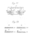
- Fig. 18 is an example of the digital gamma correction circuit 32, in which a programable read only memory (ROM) circuit 215 (such as SN74471) is used.
- ROM read only memory
- the example shows the case of 8-bit parallel input and output.
- the ROM circuit 215 With receiving 8 bits digital luminance signals 35 through terminal 216, the ROM circuit 215 produces digital luminance signals 36 at terminal 217.
- An example of the gamma corrected curve 218 is shown in Fig. 19, where E1 and E2 denote respectively analog converted value of 8-bit parallel input and 8-bit parallel output.
- the characteristic curve 218 is arbitrary program in accordance with informations 19b of a requested gamma value. It is apparent that the part of the ROM circuit 215 may be replaced with a random access memory (RAM).
- RAM random access memory
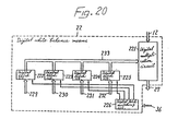
- Fig. 20 is an example of the digital white balance means 22 shown in Fig. 2.
- a digital multiplication circuit 221, first to fourth digital latch circuits 229-232, a digital switch circuit 226 are provided in the digital white balance means 22, in which four outputs of the first to fourth digital latch circuits 229-232 are connected in common with a common bus 233 and are used as an input terminal for the digital multiplication circuit 221.
- the digital switch circuit 226 controls latch up timing of the first to fourth digital latch circuits 229-232.
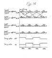
- Fig. 21(a) shows an example of partially expanded waveform for the picture-pixel signal 12 in horizontal synchronous intervals H, and H 2 .
- the digital picture-pixel signal 12 is composed of M, G, M, G informations.
- the digital switch circuit 226 latches up the first digital latch circuit 222, and the first digital latch circuit 222 transfer a multiplier value 229 used for M picture-pixel signal into the common bus 233. Therefore, a multiplication between the digital M picture-pixel signal 234 and the multiplier value 229 is performed by the digital multiplication circuit 221.
- the calculated result is recognized as a digital M picture-pixel signal 235 corrected by the multiplier value 229.
- the digital switch circuit 226 latches up the second digital latch circuit 223, and the second latch circuit 223 transfer a multiplier value 230 into the common bus 233. Therefore, a multiplication between M picture-pixel signal 234 and the multiplier value 229 is performed by the digital multiplication circuit 221. The result is recognized as a digital G picture-pixel signals 230 corrected by multiplier value 230. In this way, during the horizontal synchronous interval H i , the digital picture-pixel signal 12 with informations of M, G, M, G is converted into the digital picture-pixel signal 27 with the informations of M, G, M, G in accordance with the latch up timing for the first and second digital latch circuits 222, 223.
- the digital picture-pixel signal 12 is composed of C, Y, C, Y informations.
- the digital switch circuit 226 latches up the third digital latch circuit 224, and the third digital latch circuit 224 transfers a multiplier value 231 into the common bus 233. Therefore, a multiplication between the digital C picture-pixel signal 238 and the multiplier value 231 is performed by the digital multiplier circuits 221. The calculated result is recognized as a digital C picture pixel signal 239 corrected by multiplier value 231.
- the digital switch circuit 226 latches up the fourth digital latch circuit 225, and the fourth digital latch circuit 225 transfers a multiplier value 232 into the common bus 233.
- a multiplication between the digital Y picture-pixel signal 240 and the multiplier value 232 is performed by the digital multiplication circuit 221.
- the calculated result is recognized as a digital Y picture-pixel signal 241 corrected with the multiplier value 232.
- the digital picture-pixel signal 12 with informations of C, Y, C, Y is converted into digital picture-pixel signal 27 with informations of C, Y, C, Y.
- the digital picture-pixel signal 12 can be converted into the digital picture-pixel signal 27 with getting multiplications of the multiplier values 229, 230, 231 and 232 in accordance with the latch up timing of the first to fourth digital latch circuits 222, 223, 224 and 225.
- the timing pulse systems 36 control the digital switch circuit 226 with getting timing informations of M, G, C, Y digital picture-pixel signals, clock pulses with a repetition rate of 1lf c and horizontal synchronous intervals.
- Fig. 22 is an example of the digital white balance means 40 shown in Fig. 3.
- a first and a second digital data-process circuits 242, 243 are provided in the digital white balance means 40, in which digital correction data 244, 245 are respectively supplied to the first and second data-process digital circuits 242, 243.
- the data-path multiplex means 26 shown in Fig. 3 produces the digital chrominance difference signals 42, 43 as shown in Fig. 23(a).
- the digital chrominance difference signals 42 are composed of M-G, M-G, ... signals repeated at a rate of 1/f e and continued during each horizontal synchronous interval.
- the digital chrominance difference signal 43 is composed of C-Y, C-Y, ... signals repeated at a rate of 1/f o and continued during each horizontal synchronous interval.
- the digital data-process circuit 242 With receiving the digital chrominance difference signal 42 and the digital correction data 244 as inputs, the digital data-process circuit 242 adds the digital correction data 244 with positive or negative values to the digital chrominance difference signal 42. As the result of this data-process, the digital chrominance difference signal 14 is produced. With receiving the digital chrominance difference signal 43 and digital correction data 245 as inputs, the digital data process circuit 243 adds the digital correction data 245 with positive or negative values to the digital chrominance difference signal 43. As the result of this data-process, the digital chrominance difference signal 15 is produced. In this way, the digital chrominance difference signals 42 and 43 are respectively converted to two digital chrominance difference signals 14 and 15 by getting relatively independent values of digital correction data 244 and 245.
- the timing pulse system 41 supplied to the digital white balance means 40 corresponds to the digital correction data 244 and 245. These data can be defined with a evaluation of the chrominance difference signals 14, 15 themselves. An actually detailed method how to define the data is realized by using a microcomputer. The above described operations of the digital white balance means 40 are illustrated in Figs. 23-(a), (b).
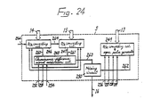
- Fig. 24 is an example of a specific configuration for the color television signal encoding means 5 shown in Figs. 1-3.
- the color television signal encoding means 5 comprises: a first digital to analog signal (D/A) converting means 246 coupled to the digital chrominance signal processing means 4 for receiving the digital chrominance difference signal 14 to produce a first analog chrominance difference signal 260; a second digital to analog signal (D/A) converting means 247 coupled to the digital chrominance signal processing means 4 for receiving the digital chrominance difference signal 15 to produce a second analog chrominance difference signal 261; a third digital to analog signal (D/A) converting means 249 coupled to the digital luminance signal processing means 3 for receiving the digital luminance signal 13 to produce an analog luminance signal 262; a modulated chrominance signal producing means 248 coupled to the first and second D/A converting means 246, 247 for receiving the first and second analog chrominance difference signals 260, 261 to produce a modulated analog
- Pulses clocking with a repetition rate of 1/f c are supplied to the first and second D/A converting means 246, 247 through a terminal 264.
- Timing pulses with vertical and horizontal blanking intervals and timing pulses with burst flag interval are supplied to the first and second D/A converting means 246, 247 and the modulated chrominance signal producing means 248 through a terminal 252 and a terminal 253.
- Burst carrier pulses with a frequency of 3.58 MHz (for NTSC case) are supplied to the modulated chrominance signal producing means 248 through a terminal 254.
- Standard bias signal for clipping black and white level timing pulses with vertical and horizontal blanking intervals, timing pulses with vertical and horizontal synchronous and clocking pulses with a repetition rate of 1/f c are respectively supplied to the'third D/A converting means 249 through terminals 256, 257, 258, 259.
- This means that functions for generating timing intervals of the standard television signals are included in the third D/A converting means 249. In this way an example of the color television encoding means 5 are realized.
Landscapes
- Engineering & Computer Science (AREA)
- Multimedia (AREA)
- Signal Processing (AREA)
- Physics & Mathematics (AREA)
- Spectroscopy & Molecular Physics (AREA)
- Processing Of Color Television Signals (AREA)
- Color Television Image Signal Generators (AREA)
Claims (19)
Applications Claiming Priority (4)
| Application Number | Priority Date | Filing Date | Title |
|---|---|---|---|
| JP196985/82 | 1982-11-10 | ||
| JP57196985A JPS5986987A (ja) | 1982-11-10 | 1982-11-10 | カラ−カメラ装置 |
| JP199190/82 | 1982-11-12 | ||
| JP57199190A JPS5989091A (ja) | 1982-11-12 | 1982-11-12 | カラ−カメラ装置 |
Publications (2)
| Publication Number | Publication Date |
|---|---|
| EP0109261A1 EP0109261A1 (de) | 1984-05-23 |
| EP0109261B1 true EP0109261B1 (de) | 1987-01-28 |
Family
ID=26510098
Family Applications (1)
| Application Number | Title | Priority Date | Filing Date |
|---|---|---|---|
| EP83306839A Expired EP0109261B1 (de) | 1982-11-10 | 1983-11-09 | Farbfernsehkamera |
Country Status (3)
| Country | Link |
|---|---|
| US (1) | US4620222A (de) |
| EP (1) | EP0109261B1 (de) |
| DE (1) | DE3369622D1 (de) |
Families Citing this family (26)
| Publication number | Priority date | Publication date | Assignee | Title |
|---|---|---|---|---|
| US4599640A (en) * | 1984-02-29 | 1986-07-08 | Rca Corporation | Television camera with multiplexed A-D converter |
| JPS60194889A (ja) * | 1984-03-16 | 1985-10-03 | Toshiba Corp | カラ−固体撮像装置 |
| US4837614A (en) * | 1986-08-20 | 1989-06-06 | Ricoh Company, Ltd. | Color image processing method |
| JPS63233693A (ja) * | 1987-03-23 | 1988-09-29 | Hitachi Ltd | 固体カラ−カメラの信号処理装置 |
| EP0323194A3 (de) * | 1987-12-25 | 1991-07-10 | Kabushiki Kaisha Toshiba | Elektronische Stehbildkamera und Bildaufzeichnungsverfahren dazu |
| US5008739A (en) * | 1989-02-13 | 1991-04-16 | Eastman Kodak Company | Real-time digital processor for producing full resolution color signals from a multi-color image sensor |
| US5331223A (en) * | 1989-08-25 | 1994-07-19 | Teac Corporation | Signal supplying unit having means for selecting signal in accordance with terminal connection |
| EP0720389B1 (de) * | 1990-10-31 | 2001-04-04 | Hitachi, Ltd. | Zittervermeidung im Videokameraausgabebild |
| US5293225A (en) * | 1991-05-31 | 1994-03-08 | Victor Company Of Japan, Ltd. | Digital signal processing system for color camera apparatus including separate delays for color signal and brightness signal processing |
| KR940008842B1 (ko) * | 1991-11-27 | 1994-09-26 | 삼성전자 주식회사 | 디지틀 엔코더 |
| US5345265A (en) * | 1992-12-31 | 1994-09-06 | Samsung Electronics Co., Ltd. | Gamma correction circuit for a video camera |
| JP3937458B2 (ja) * | 1993-03-05 | 2007-06-27 | キヤノン株式会社 | 撮像装置 |
| JP3615778B2 (ja) * | 1993-04-05 | 2005-02-02 | 日本フィリップス株式会社 | カラー撮像装置 |
| US8405727B2 (en) * | 2008-05-01 | 2013-03-26 | Apple Inc. | Apparatus and method for calibrating image capture devices |
| US8538084B2 (en) * | 2008-09-08 | 2013-09-17 | Apple Inc. | Method and apparatus for depth sensing keystoning |
| US8508671B2 (en) | 2008-09-08 | 2013-08-13 | Apple Inc. | Projection systems and methods |
| US20100079426A1 (en) * | 2008-09-26 | 2010-04-01 | Apple Inc. | Spatial ambient light profiling |
| US8610726B2 (en) * | 2008-09-26 | 2013-12-17 | Apple Inc. | Computer systems and methods with projected display |
| US7881603B2 (en) * | 2008-09-26 | 2011-02-01 | Apple Inc. | Dichroic aperture for electronic imaging device |
| US8527908B2 (en) | 2008-09-26 | 2013-09-03 | Apple Inc. | Computer user interface system and methods |
| US8619128B2 (en) | 2009-09-30 | 2013-12-31 | Apple Inc. | Systems and methods for an imaging system using multiple image sensors |
| US8502926B2 (en) * | 2009-09-30 | 2013-08-06 | Apple Inc. | Display system having coherent and incoherent light sources |
| US8687070B2 (en) * | 2009-12-22 | 2014-04-01 | Apple Inc. | Image capture device having tilt and/or perspective correction |
| US8497897B2 (en) | 2010-08-17 | 2013-07-30 | Apple Inc. | Image capture using luminance and chrominance sensors |
| US8538132B2 (en) | 2010-09-24 | 2013-09-17 | Apple Inc. | Component concentricity |
| US9356061B2 (en) | 2013-08-05 | 2016-05-31 | Apple Inc. | Image sensor with buried light shield and vertical gate |
Family Cites Families (7)
| Publication number | Priority date | Publication date | Assignee | Title |
|---|---|---|---|---|
| DE2518247C3 (de) * | 1975-04-24 | 1978-04-20 | Siemens Ag, 1000 Berlin Und 8000 Muenchen | Verfahren und Schaltungsanordnung zum Decodieren des Ausgangssignals einer Bildaufnahmeröhre in einer Einröhren-Farbfernsehkamera |
| GB2014397B (en) * | 1978-02-10 | 1982-08-18 | Hitachi Ltd | Solid-state colour imaging device |
| JPS56109087A (en) * | 1980-01-31 | 1981-08-29 | Sony Corp | Digital color encoder |
| JPS57109488A (en) * | 1980-12-26 | 1982-07-07 | Matsushita Electric Ind Co Ltd | Solid color image pickup device |
| US4345270A (en) * | 1981-01-27 | 1982-08-17 | Sony Corporation | Solid state digital television camera |
| JPS57131185A (en) * | 1981-02-06 | 1982-08-13 | Hitachi Ltd | Color image pickup device |
| JPS581391A (ja) * | 1981-06-26 | 1983-01-06 | Sony Corp | 固体カラー撮像装置 |
-
1983
- 1983-11-08 US US06/549,812 patent/US4620222A/en not_active Expired - Lifetime
- 1983-11-09 DE DE8383306839T patent/DE3369622D1/de not_active Expired
- 1983-11-09 EP EP83306839A patent/EP0109261B1/de not_active Expired
Also Published As
| Publication number | Publication date |
|---|---|
| DE3369622D1 (en) | 1987-03-05 |
| EP0109261A1 (de) | 1984-05-23 |
| US4620222A (en) | 1986-10-28 |
Similar Documents
| Publication | Publication Date | Title |
|---|---|---|
| EP0109261B1 (de) | Farbfernsehkamera | |
| CA1173954A (en) | Television receiver including a circuit for doubling line scanning frequency | |
| EP0796008B1 (de) | Kamera mit digitaler und analoger Klemmschaltung | |
| US6304292B1 (en) | Digital video camera with high-speed mode | |
| EP0092973B1 (de) | Gerät zur Videoauflösung von Graphiken | |
| KR100301886B1 (ko) | 고체촬상장치및그구동방법 | |
| US5319451A (en) | Color signal processing apparatus using a common low pass filter for the luminance signal and the color signals | |
| US4117510A (en) | Solid state color imaging apparatus | |
| US6346969B1 (en) | Color filter array and its color interpolation apparatus | |
| US4894794A (en) | System for providing continous linear interpolation | |
| GB1525634A (en) | Television cameras | |
| JPS6324767A (ja) | テレビジョン画像表示装置 | |
| US4227206A (en) | Solid state television camera | |
| EP0088583A1 (de) | Bildverarbeitungseinrichtung | |
| US4761689A (en) | Apparatus for driving a solid state image pickup device | |
| US4220971A (en) | Reciprocating dropout compensator | |
| JPS6345153B2 (de) | ||
| US7751097B2 (en) | Methods and apparatuses for changing driving sequence to output charge coupled device signal | |
| US5229859A (en) | Image pickup apparatus for full line reading | |
| US6266101B1 (en) | Y/C separator | |
| JP2840236B2 (ja) | カラー画像情報伝送装置 | |
| JP2670200B2 (ja) | 画像データ再生装置における間引回路 | |
| SU1665391A1 (ru) | Система ввода телевизионных изображений в ЭВМ | |
| KR100376957B1 (ko) | 화상 데이타의 처리 방법 및 화상 데이타 처리 장치 | |
| JPS5989091A (ja) | カラ−カメラ装置 |
Legal Events
| Date | Code | Title | Description |
|---|---|---|---|
| PUAI | Public reference made under article 153(3) epc to a published international application that has entered the european phase |
Free format text: ORIGINAL CODE: 0009012 |
|
| AK | Designated contracting states |
Designated state(s): DE FR GB |
|
| 17P | Request for examination filed |
Effective date: 19841121 |
|
| GRAA | (expected) grant |
Free format text: ORIGINAL CODE: 0009210 |
|
| AK | Designated contracting states |
Kind code of ref document: B1 Designated state(s): DE FR GB |
|
| ET | Fr: translation filed | ||
| REF | Corresponds to: |
Ref document number: 3369622 Country of ref document: DE Date of ref document: 19870305 |
|
| PLBE | No opposition filed within time limit |
Free format text: ORIGINAL CODE: 0009261 |
|
| STAA | Information on the status of an ep patent application or granted ep patent |
Free format text: STATUS: NO OPPOSITION FILED WITHIN TIME LIMIT |
|
| 26N | No opposition filed | ||
| PGFP | Annual fee paid to national office [announced via postgrant information from national office to epo] |
Ref country code: FR Payment date: 19981110 Year of fee payment: 16 |
|
| PGFP | Annual fee paid to national office [announced via postgrant information from national office to epo] |
Ref country code: GB Payment date: 19981113 Year of fee payment: 16 |
|
| PGFP | Annual fee paid to national office [announced via postgrant information from national office to epo] |
Ref country code: DE Payment date: 19981116 Year of fee payment: 16 |
|
| PG25 | Lapsed in a contracting state [announced via postgrant information from national office to epo] |
Ref country code: GB Free format text: LAPSE BECAUSE OF NON-PAYMENT OF DUE FEES Effective date: 19991109 |
|
| GBPC | Gb: european patent ceased through non-payment of renewal fee |
Effective date: 19991109 |
|
| PG25 | Lapsed in a contracting state [announced via postgrant information from national office to epo] |
Ref country code: FR Free format text: LAPSE BECAUSE OF NON-PAYMENT OF DUE FEES Effective date: 20000731 |
|
| PG25 | Lapsed in a contracting state [announced via postgrant information from national office to epo] |
Ref country code: DE Free format text: LAPSE BECAUSE OF NON-PAYMENT OF DUE FEES Effective date: 20000901 |
|
| REG | Reference to a national code |
Ref country code: FR Ref legal event code: ST |