EP0766404A2 - Taktgenerator mit einer Phasenregelkreisschaltung - Google Patents
Taktgenerator mit einer Phasenregelkreisschaltung Download PDFInfo
- Publication number
- EP0766404A2 EP0766404A2 EP96112718A EP96112718A EP0766404A2 EP 0766404 A2 EP0766404 A2 EP 0766404A2 EP 96112718 A EP96112718 A EP 96112718A EP 96112718 A EP96112718 A EP 96112718A EP 0766404 A2 EP0766404 A2 EP 0766404A2
- Authority
- EP
- European Patent Office
- Prior art keywords
- clock signal
- frequency
- clock
- divider
- output
- Prior art date
- Legal status (The legal status is an assumption and is not a legal conclusion. Google has not performed a legal analysis and makes no representation as to the accuracy of the status listed.)
- Withdrawn
Links
Images
Classifications
-
- H—ELECTRICITY
- H03—ELECTRONIC CIRCUITRY
- H03L—AUTOMATIC CONTROL, STARTING, SYNCHRONISATION, OR STABILISATION OF GENERATORS OF ELECTRONIC OSCILLATIONS OR PULSES
- H03L7/00—Automatic control of frequency or phase; Synchronisation
- H03L7/06—Automatic control of frequency or phase; Synchronisation using a reference signal applied to a frequency- or phase-locked loop
- H03L7/16—Indirect frequency synthesis, i.e. generating a desired one of a number of predetermined frequencies using a frequency- or phase-locked loop
- H03L7/18—Indirect frequency synthesis, i.e. generating a desired one of a number of predetermined frequencies using a frequency- or phase-locked loop using a frequency divider or counter in the loop
-
- H—ELECTRICITY
- H03—ELECTRONIC CIRCUITRY
- H03K—PULSE TECHNIQUE
- H03K23/00—Pulse counters comprising counting chains; Frequency dividers comprising counting chains
- H03K23/64—Pulse counters comprising counting chains; Frequency dividers comprising counting chains with a base or radix other than a power of two
- H03K23/66—Pulse counters comprising counting chains; Frequency dividers comprising counting chains with a base or radix other than a power of two with a variable counting base, e.g. by presetting or by adding or suppressing pulses
- H03K23/667—Pulse counters comprising counting chains; Frequency dividers comprising counting chains with a base or radix other than a power of two with a variable counting base, e.g. by presetting or by adding or suppressing pulses by switching the base during a counting cycle
-
- H—ELECTRICITY
- H03—ELECTRONIC CIRCUITRY
- H03L—AUTOMATIC CONTROL, STARTING, SYNCHRONISATION, OR STABILISATION OF GENERATORS OF ELECTRONIC OSCILLATIONS OR PULSES
- H03L7/00—Automatic control of frequency or phase; Synchronisation
- H03L7/06—Automatic control of frequency or phase; Synchronisation using a reference signal applied to a frequency- or phase-locked loop
- H03L7/16—Indirect frequency synthesis, i.e. generating a desired one of a number of predetermined frequencies using a frequency- or phase-locked loop
- H03L7/18—Indirect frequency synthesis, i.e. generating a desired one of a number of predetermined frequencies using a frequency- or phase-locked loop using a frequency divider or counter in the loop
- H03L7/183—Indirect frequency synthesis, i.e. generating a desired one of a number of predetermined frequencies using a frequency- or phase-locked loop using a frequency divider or counter in the loop a time difference being used for locking the loop, the counter counting between fixed numbers or the frequency divider dividing by a fixed number
Definitions
- the present invention relates to a clock generator for generating and supplying a clock signal to a data processing unit such as a control processing unit (CPU) and, more particularly, to such a clock generator that utilizes a phase locked loop (PLL) circuit to generating a clock signal having a desired clock rate or frequency.
- a data processing unit such as a control processing unit (CPU)
- PLL phase locked loop
- the clock generator is further required to change the frequency of the system clock signal.
- the system clock signal In a standby mode, for example, the system clock signal is lowered in frequency to thereby reduce power consumption.
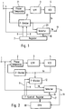
- Japanese Patent Laid-Open Publucation Hei 4-12842 presents a certain clock generator, which is shown in Fig. 1.
- This clock generator includes a clock input terminal 1 supplied with a clock signal from a crystal oscillator (not shown).
- the terminal 1 is in turn connected as a reference clock input to one input node of a phase detector 21 of a PLL circuit 20.
- the output of the phase detector 21 is connected to a low-pass filter 3 which responds thereto and produces a control voltage to control the oscillation frequency of a voltage-controlled oscillator (VCO) 4.
- VCO voltage-controlled oscillator
- the output of the voltage control oscillator 4 is supplied to a modulo divider 22.
- the divider 22 frequency-divides the output of the VCO 4 and supplies the other input node of the phase detector 21 with the divided signal.
- the frequency-division ratio of the divider is controlled or changed by control signals 8 and 9 outputted from a frequency control register 7.
- This register 7 further outputs a clock selector signal 10 to a selector 23 which receives the signals from the terminal 1 and the VCO 4.
- the selector 23 selects and outputs one of the signals of the terminal 1 and the VCO 4 at an output terminal 11.
- the clock signal derived from the terminal 11 is supplied to a CPU (not shown) as a system clock signal.
- the VCO output becomes 10 MHz is frequency.
- the division ratio being 5 by the control signal 9
- the VCO output becomes 25 MHz in frequency.
- the CPU clock takes 5 MHz, 10 MHz or 25 MHz in accordance with the contents of the control signals 8 - 10.
- the above clock generator can generate such a clock signal that is higher in requency than the input clock signal and further can control the frequence of an actual system or CPU clock signal.
- the so-called lock-up time is needed for the PLL 20 to be stable and to oscillate at a desired frequency.
- This lock-up time is caused by bandwidth characteristics of the loop, namely, bandwidth characteristics of the low-pass filter 3.
- bandwidth characteristics of the loop namely, bandwidth characteristics of the low-pass filter 3.
- the lock-up time is shortened but the jitter is made greater, so a CPU clock fc which is stable in frequency and duty cannot be obtained.
- a clock generator utilized a PLL circuit to generate a first clock signal relative to an input clock signal and further includes a frequency divider which is provided outside the loop of the PLL circuit to receive the first clock signal.
- the frequency-division ratio of the divider is controlled by a set of control signals to produce an output clock signal having a variable or controllable frequency.
- the change in frequency-division ratio of the divider gives no effect to the PLL loop. That is, the PLL circuit is in a stable state irrespective of whether or not the divider is changed in frequency-division ratio. Accordingly, the output clock is changed in frequency without requiring the lock-up time of the PLL circuit.
- a clock generator utilizes a PLL circuit 20.
- This circuit 20 includes an input terminal 1 supplied with an input clock signal from a quartz-crystal oscillator or an external system (both not shown) as a reference clock, that terminal 1 being connected to one input side of a phase and/or frequency comparator 2.
- the output of the comparator 2 is supplied to a low-pass filter 3 whose output signal is in turn supplied a voltage controlled oscillator (VCO) 4 to control the oscillation frequency thereof.
- VCO voltage controlled oscillator
- the signal from the VCO 4 is supplied to and thus frequency-divided by a frequency divider 5.
- the frequency-divided output of the divider 5 is fed back to the other input side of the phase comparator 2.
- the output signal of the VCO 4 is further supplied to a frequency divider 12 which is provided in accordance with the present invention.
- This divider 12 can take in the present embodiment two frequency-division ratio in accordance with the contents of control signals 8 and 9 which are supplied from a frequency control register 7.
- the divide 12 includes a J-K flip-flops 12-1, two AND gates 12-3 and 12-4 and an OR gate 12-5, which are connected as shown. Accordingly, when the control signals 8 and 9 takes “0" and “1", respectively, the frequency-division ratio N of the divider 12 becomes 1. In the case of the signals 8 and 9 takes respectively "1" and "0", the divider 12 takes the division ratio N of 2.
- the output signal of the divider 12 is supplied to a clock selector 6 together with the input clock signal.
- the clock selector 6 selects the output of the divider 12 when the control signal 10 assumes the high level and the input clock signal when the control signal 10 assumes the low level.
- the control signal 10 is also supplied from the register 10.
- the clock signal thus selected by the selector 6 is supplied to a CPU 50 as a system or CPU clock signal 11.
- the CPU 50 operates based upon the clock signal 11 to execute each instruction and process data. Further, the CPU 50 controls the register 7 to change the contents thereof.
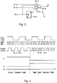
- the CPU 50 is operable in three modes. These three modes consist of a normal operation mode, a high speed operation mode and a standby mode.
- control signals 8, 9 and 10 takes “1", “0” and “1", respectively, as shown in Fig 4.
- the frequency-division ratio N of the divider 12 thereby becomes 2 and the clock selector 6 selects and outputs the signal from the divider 12 as the system clock signal 11.
- This signal has a frequency fc of 12.5 MHz.
- the CPU 50 operates based upon this system clock 11.
- the CPU 50 When an external event happens at this time, which even requires the CPU 50 of performing a data operation at a high speed, the CPU 50 rewrites the frequency control register 7 such that the control set so that the signals 8, 9 and 10 takes “0", "1" and "1", respectively, as shown in Fig. 2. As a result, the division ratio N of the divider 12 is switched to 1. The output of the divider 12 is thereby immediately switched to 25 MHz and the system clock 11 is also changed to 25 MHz in an instant. The CPU 11 operates on the system clock signal of 25 MHz as the high speed operation mode.
- the CPU 11 changes the signal 10 to the low level, so that the system clock signal 11 is changed to be 5 MHz. Power consumption is thereby reduced.
- the frequency divider 12 is switched between two states but it is possible to obtain various clocks lower than a frequency outputted from the VCO 4 by setting three or more division ratios into the divider 12. That is, the present invention is not limited to the above embodiment, but may be changed and modified without departing the scope and spirit of the invention.
Applications Claiming Priority (2)
| Application Number | Priority Date | Filing Date | Title |
|---|---|---|---|
| JP7250631A JPH0993126A (ja) | 1995-09-28 | 1995-09-28 | クロック発生器 |
| JP250631/95 | 1995-09-28 |
Publications (2)
| Publication Number | Publication Date |
|---|---|
| EP0766404A2 true EP0766404A2 (de) | 1997-04-02 |
| EP0766404A3 EP0766404A3 (de) | 1998-01-07 |
Family
ID=17210733
Family Applications (1)
| Application Number | Title | Priority Date | Filing Date |
|---|---|---|---|
| EP96112718A Withdrawn EP0766404A3 (de) | 1995-09-28 | 1996-08-07 | Taktgenerator mit einer Phasenregelkreisschaltung |
Country Status (3)
| Country | Link |
|---|---|
| EP (1) | EP0766404A3 (de) |
| JP (1) | JPH0993126A (de) |
| KR (1) | KR970019089A (de) |
Cited By (9)
| Publication number | Priority date | Publication date | Assignee | Title |
|---|---|---|---|---|
| EP0881775A1 (de) * | 1997-05-30 | 1998-12-02 | Nec Corporation | Taktgenerator |
| EP0895358A2 (de) * | 1997-07-28 | 1999-02-03 | Motorola, Inc. | Verfahren und System zum Erzeugen eines Prozessortaktes mit schnellem Startvorgang |
| WO1999021280A1 (en) * | 1997-10-16 | 1999-04-29 | Oasis Design, Inc. | Phase-locked loop and integrated circuit therefor |
| EP1039641A1 (de) * | 1999-03-15 | 2000-09-27 | Alcatel | Verfahren zur Herstellung eines Taktsignales und Vorrichtung dazu |
| WO2002017052A2 (en) * | 2000-08-21 | 2002-02-28 | Intel Corporation | Apparatus having adjustable operational modes and method therefore |
| EP1253505A2 (de) * | 2001-04-26 | 2002-10-30 | Nec Corporation | Taktverteilerschaltung |
| CN100371857C (zh) * | 2003-11-04 | 2008-02-27 | 上海华虹集成电路有限责任公司 | 一种防简单功耗分析攻击的方法 |
| US11695421B1 (en) | 2022-01-14 | 2023-07-04 | Changxin Memory Technologies, Inc. | Delay-locked loop, control method for delay-locked loop, and electronic device |
| WO2023134034A1 (zh) * | 2022-01-14 | 2023-07-20 | 长鑫存储技术有限公司 | 延迟锁相环、延迟锁相环控制方法及电子设备 |
Families Citing this family (2)
| Publication number | Priority date | Publication date | Assignee | Title |
|---|---|---|---|---|
| KR100651510B1 (ko) * | 2005-01-17 | 2006-11-29 | 삼성전기주식회사 | 동적 클럭 전환 장치 및 그 방법 |
| KR101591338B1 (ko) * | 2009-03-30 | 2016-02-19 | 삼성전자주식회사 | 롱 텀 지터를 최소화 한 클럭발생기 |
Citations (5)
| Publication number | Priority date | Publication date | Assignee | Title |
|---|---|---|---|---|
| JPS6020223A (ja) * | 1983-07-15 | 1985-02-01 | Hitachi Ltd | Cmos半導体集積回路装置 |
| US4893271A (en) * | 1983-11-07 | 1990-01-09 | Motorola, Inc. | Synthesized clock microcomputer with power saving |
| EP0385567A2 (de) * | 1989-02-28 | 1990-09-05 | International Business Machines Corporation | Taktsignalgenerator für ein Datenverarbeitungssystem |
| EP0645689A2 (de) * | 1993-09-29 | 1995-03-29 | Seiko Epson Corporation | Taktversorgungsystem, Echtzeittaktmodul und Taktgeber |
| US5406590A (en) * | 1992-10-23 | 1995-04-11 | Compaq Computer Corporation | Method of and apparatus for correcting edge placement errors in multiplying phase locked loop circuits |
Family Cites Families (3)
| Publication number | Priority date | Publication date | Assignee | Title |
|---|---|---|---|---|
| JPS6458117A (en) * | 1987-08-28 | 1989-03-06 | Yokogawa Electric Corp | Digital signal generator |
| JPH03198424A (ja) * | 1989-12-27 | 1991-08-29 | Fujitsu Ltd | 周波数シンセサイザ |
| JP2976723B2 (ja) * | 1992-10-08 | 1999-11-10 | 日本電気株式会社 | 半導体装置 |
-
1995
- 1995-09-28 JP JP7250631A patent/JPH0993126A/ja active Pending
-
1996
- 1996-08-07 EP EP96112718A patent/EP0766404A3/de not_active Withdrawn
- 1996-08-26 KR KR1019960035555A patent/KR970019089A/ko not_active Application Discontinuation
Patent Citations (5)
| Publication number | Priority date | Publication date | Assignee | Title |
|---|---|---|---|---|
| JPS6020223A (ja) * | 1983-07-15 | 1985-02-01 | Hitachi Ltd | Cmos半導体集積回路装置 |
| US4893271A (en) * | 1983-11-07 | 1990-01-09 | Motorola, Inc. | Synthesized clock microcomputer with power saving |
| EP0385567A2 (de) * | 1989-02-28 | 1990-09-05 | International Business Machines Corporation | Taktsignalgenerator für ein Datenverarbeitungssystem |
| US5406590A (en) * | 1992-10-23 | 1995-04-11 | Compaq Computer Corporation | Method of and apparatus for correcting edge placement errors in multiplying phase locked loop circuits |
| EP0645689A2 (de) * | 1993-09-29 | 1995-03-29 | Seiko Epson Corporation | Taktversorgungsystem, Echtzeittaktmodul und Taktgeber |
Non-Patent Citations (1)
| Title |
|---|
| PATENT ABSTRACTS OF JAPAN vol. 9, no. 141 (P-364), 15 June 1985 & JP 60 020223 A (HITACHI SEISAKUSHO KK), 1 February 1985, * |
Cited By (17)
| Publication number | Priority date | Publication date | Assignee | Title |
|---|---|---|---|---|
| EP0881775A1 (de) * | 1997-05-30 | 1998-12-02 | Nec Corporation | Taktgenerator |
| EP0895358A2 (de) * | 1997-07-28 | 1999-02-03 | Motorola, Inc. | Verfahren und System zum Erzeugen eines Prozessortaktes mit schnellem Startvorgang |
| EP0895358A3 (de) * | 1997-07-28 | 1999-04-14 | Motorola, Inc. | Verfahren und System zum Erzeugen eines Prozessortaktes mit schnellem Startvorgang |
| WO1999021280A1 (en) * | 1997-10-16 | 1999-04-29 | Oasis Design, Inc. | Phase-locked loop and integrated circuit therefor |
| US6005904A (en) * | 1997-10-16 | 1999-12-21 | Oasis Design, Inc. | Phase-locked loop with protected output during instances when the phase-locked loop is unlocked |
| EP1039641A1 (de) * | 1999-03-15 | 2000-09-27 | Alcatel | Verfahren zur Herstellung eines Taktsignales und Vorrichtung dazu |
| US6335644B1 (en) | 1999-03-15 | 2002-01-01 | Alcatel | Method for synthesizing a clock signal and synthesizing device thereof |
| CN100409144C (zh) * | 2000-08-21 | 2008-08-06 | 英特尔公司 | 具有可调工作模式的装置 |
| WO2002017052A2 (en) * | 2000-08-21 | 2002-02-28 | Intel Corporation | Apparatus having adjustable operational modes and method therefore |
| WO2002017052A3 (en) * | 2000-08-21 | 2003-03-27 | Intel Corp | Apparatus having adjustable operational modes and method therefore |
| US6664775B1 (en) | 2000-08-21 | 2003-12-16 | Intel Corporation | Apparatus having adjustable operational modes and method therefore |
| US6949918B2 (en) | 2000-08-21 | 2005-09-27 | Intel Corporation | Apparatus having adjustable operational modes and method therefore |
| EP1253505A2 (de) * | 2001-04-26 | 2002-10-30 | Nec Corporation | Taktverteilerschaltung |
| EP1253505A3 (de) * | 2001-04-26 | 2009-06-17 | NEC Electronics Corporation | Taktverteilerschaltung |
| CN100371857C (zh) * | 2003-11-04 | 2008-02-27 | 上海华虹集成电路有限责任公司 | 一种防简单功耗分析攻击的方法 |
| US11695421B1 (en) | 2022-01-14 | 2023-07-04 | Changxin Memory Technologies, Inc. | Delay-locked loop, control method for delay-locked loop, and electronic device |
| WO2023134034A1 (zh) * | 2022-01-14 | 2023-07-20 | 长鑫存储技术有限公司 | 延迟锁相环、延迟锁相环控制方法及电子设备 |
Also Published As
| Publication number | Publication date |
|---|---|
| JPH0993126A (ja) | 1997-04-04 |
| EP0766404A3 (de) | 1998-01-07 |
| KR970019089A (ko) | 1997-04-30 |
Similar Documents
| Publication | Publication Date | Title |
|---|---|---|
| US5838178A (en) | Phase-locked loop and resulting frequency multiplier | |
| KR970002219B1 (ko) | 최적 조정 및 레벨형 동기 표시를 구현한 디지탈 위상 검출기를 가진 주파수 합성기 | |
| EP0800276B1 (de) | Frequenzvervielfacher, bei dem das Multiplikationsverhältnis in der ersten Stufe grösser ist als in den nachfolgenden Stufen | |
| EP0604043A1 (de) | Digitaler Frequenzdetektor mit grossem Bereich | |
| JP3320353B2 (ja) | 可変速度位相ロック・ループ・システムおよびその方法 | |
| KR0138220B1 (ko) | 위상동기루프회로의 클럭지연보상 및 듀티제어 장치 | |
| US5663687A (en) | LSI with built-in clock generator-controller for operation with low power dissipation | |
| EP0766404A2 (de) | Taktgenerator mit einer Phasenregelkreisschaltung | |
| US5438300A (en) | Digital frequency multiplier utilizing digital controlled oscillator | |
| US20070201594A1 (en) | Phase Locked Loop (Pll) Circuit, Its Phasing Method And Operation Analyzing Method | |
| EP0881775A1 (de) | Taktgenerator | |
| GB2236922A (en) | Frequency synthesisers | |
| JPH10143272A (ja) | 発振回路 | |
| US5867545A (en) | Phase-locked loop circuit | |
| KR960000053Y1 (ko) | 대역가변 dpll회로 | |
| KR200291191Y1 (ko) | 가변클럭발생기 | |
| JP2998716B2 (ja) | フレーム同期制御回路 | |
| JP3248453B2 (ja) | 発振装置 | |
| JPS62128211A (ja) | 周波数シンセサイザ | |
| JP3160904B2 (ja) | 位相同期発振回路装置 | |
| JPH10289032A (ja) | 半導体集積回路のクロック回路 | |
| JPH1132359A (ja) | ページャ | |
| JP2911276B2 (ja) | Pll周波数シンセサイザ回路 | |
| JP2001527313A (ja) | 位相同期ループ周波数発生源におけるロードプルを減少させる方法と装置 | |
| JPH04110029U (ja) | 位相同期発振回路 |
Legal Events
| Date | Code | Title | Description |
|---|---|---|---|
| PUAI | Public reference made under article 153(3) epc to a published international application that has entered the european phase |
Free format text: ORIGINAL CODE: 0009012 |
|
| AK | Designated contracting states |
Kind code of ref document: A2 Designated state(s): DE GB NL |
|
| PUAL | Search report despatched |
Free format text: ORIGINAL CODE: 0009013 |
|
| AK | Designated contracting states |
Kind code of ref document: A3 Designated state(s): DE GB NL |
|
| 17P | Request for examination filed |
Effective date: 19980707 |
|
| STAA | Information on the status of an ep patent application or granted ep patent |
Free format text: STATUS: THE APPLICATION HAS BEEN WITHDRAWN |
|
| 18W | Application withdrawn |
Withdrawal date: 19990127 |