EP0895358A2 - Verfahren und System zum Erzeugen eines Prozessortaktes mit schnellem Startvorgang - Google Patents
Verfahren und System zum Erzeugen eines Prozessortaktes mit schnellem Startvorgang Download PDFInfo
- Publication number
- EP0895358A2 EP0895358A2 EP98112947A EP98112947A EP0895358A2 EP 0895358 A2 EP0895358 A2 EP 0895358A2 EP 98112947 A EP98112947 A EP 98112947A EP 98112947 A EP98112947 A EP 98112947A EP 0895358 A2 EP0895358 A2 EP 0895358A2
- Authority
- EP
- European Patent Office
- Prior art keywords
- signal
- pll
- frequency
- clock
- generating
- Prior art date
- Legal status (The legal status is an assumption and is not a legal conclusion. Google has not performed a legal analysis and makes no representation as to the accuracy of the status listed.)
- Granted
Links
- 238000000034 method Methods 0.000 title claims description 10
- 230000009977 dual effect Effects 0.000 description 7
- 230000001413 cellular effect Effects 0.000 description 5
- 230000007704 transition Effects 0.000 description 4
- 230000006870 function Effects 0.000 description 3
- 230000003247 decreasing effect Effects 0.000 description 1
- 230000001934 delay Effects 0.000 description 1
- 238000012986 modification Methods 0.000 description 1
- 230000004048 modification Effects 0.000 description 1
Images

Classifications
-
- H—ELECTRICITY
- H03—ELECTRONIC CIRCUITRY
- H03L—AUTOMATIC CONTROL, STARTING, SYNCHRONISATION OR STABILISATION OF GENERATORS OF ELECTRONIC OSCILLATIONS OR PULSES
- H03L7/00—Automatic control of frequency or phase; Synchronisation
- H03L7/06—Automatic control of frequency or phase; Synchronisation using a reference signal applied to a frequency- or phase-locked loop
- H03L7/08—Details of the phase-locked loop
- H03L7/085—Details of the phase-locked loop concerning mainly the frequency- or phase-detection arrangement including the filtering or amplification of its output signal
- H03L7/095—Details of the phase-locked loop concerning mainly the frequency- or phase-detection arrangement including the filtering or amplification of its output signal using a lock detector
-
- G—PHYSICS
- G06—COMPUTING; CALCULATING OR COUNTING
- G06F—ELECTRIC DIGITAL DATA PROCESSING
- G06F1/00—Details not covered by groups G06F3/00 - G06F13/00 and G06F21/00
- G06F1/04—Generating or distributing clock signals or signals derived directly therefrom
- G06F1/08—Clock generators with changeable or programmable clock frequency
-
- H—ELECTRICITY
- H03—ELECTRONIC CIRCUITRY
- H03L—AUTOMATIC CONTROL, STARTING, SYNCHRONISATION OR STABILISATION OF GENERATORS OF ELECTRONIC OSCILLATIONS OR PULSES
- H03L7/00—Automatic control of frequency or phase; Synchronisation
- H03L7/06—Automatic control of frequency or phase; Synchronisation using a reference signal applied to a frequency- or phase-locked loop
- H03L7/08—Details of the phase-locked loop
- H03L7/0802—Details of the phase-locked loop the loop being adapted for reducing power consumption
-
- H—ELECTRICITY
- H03—ELECTRONIC CIRCUITRY
- H03L—AUTOMATIC CONTROL, STARTING, SYNCHRONISATION OR STABILISATION OF GENERATORS OF ELECTRONIC OSCILLATIONS OR PULSES
- H03L7/00—Automatic control of frequency or phase; Synchronisation
- H03L7/06—Automatic control of frequency or phase; Synchronisation using a reference signal applied to a frequency- or phase-locked loop
- H03L7/08—Details of the phase-locked loop
- H03L7/10—Details of the phase-locked loop for assuring initial synchronisation or for broadening the capture range
- H03L7/107—Details of the phase-locked loop for assuring initial synchronisation or for broadening the capture range using a variable transfer function for the loop, e.g. low pass filter having a variable bandwidth
-
- H—ELECTRICITY
- H03—ELECTRONIC CIRCUITRY
- H03L—AUTOMATIC CONTROL, STARTING, SYNCHRONISATION OR STABILISATION OF GENERATORS OF ELECTRONIC OSCILLATIONS OR PULSES
- H03L7/00—Automatic control of frequency or phase; Synchronisation
- H03L7/06—Automatic control of frequency or phase; Synchronisation using a reference signal applied to a frequency- or phase-locked loop
- H03L7/16—Indirect frequency synthesis, i.e. generating a desired one of a number of predetermined frequencies using a frequency- or phase-locked loop
- H03L7/18—Indirect frequency synthesis, i.e. generating a desired one of a number of predetermined frequencies using a frequency- or phase-locked loop using a frequency divider or counter in the loop
Definitions
- the present invention relates in general to a phase-locked loop (PLL) based clock generation system, and in particular the present invention relates to a dual bandwidth PLL based clock generation system such as those used in battery powered devices.
- PLL phase-locked loop
- the PLL When reacquiring phase-lock after being reenabled or at startup of the system, the PLL will overshoot the target frequency when initially attempting to acquire the programmed system frequency. If the PLL's targeted output frequency is at the maximum specified frequency of the system's processor, the PLL overshoot will cause memory access failures or execution failures in the processor. To prevent these problems in prior art systems, execution control circuitry is included that delays execution within the system's processor until after the PLL acquires phase-lock.
- a portable device is consuming battery power at an operational level during this delay without the processor being operational. Therefore, it would be desirable to provide a PLL clock generation system that does not introduce the delay in processor execution without risk of overshoot related failures, thus decreasing the time spent in a full power mode.
- the present invention provides dual bandwidth PLL circuitry that allows an associated central processing unit (CPU) to begin execution of instructions prior to acquiring phase/frequency-lock.
- CPU central processing unit
- the present invention substantially enhances the power savings of the portable battery by allowing the processor to operate during the phase/frequency-locking phase of the PLL.
- a reduction of overall system power is achieved by increasing the time spent in the power saving mode. This is especially useful in applications where the system is repeatedly brought from a low power mode to an active mode such as in cellular phones, which periodically query the cellular system.
- a microcontroller based system 100 includes a dual bandwidth PLL clock generation circuit 105.
- a dual bandwidth PLL is used in systems requiring a fast startup time but having a low frequency input reference to the PLL, for example.
- a dual bandwidth PLL has two phases of operation: 1) a wide bandwidth (high gain) phase and 2) a narrow bandwidth (low gain) phase.
- a low frequency reference clock (REF) is input into PLL 110 within circuit 105, which synthesizes the reference clock to produce the PLL circuit output (PLL CLOCK) as a function of a multiplication factor input (N).
- PLL 110 is a dual bandwidth PLL to decrease lock time.
- PLL 110 outputs the PLL CLOCK to a divider 130 and outputs a FREQUENCY Lock signal to a counter 120.
- the FREQUENCY LOCK signal indicates when the PLL clock has reached the programmed frequency of the PLL to within a selected bandwidth, while the PLL is operating in a wide bandwidth mode.
- an empirically derived settling time for example 10 milliseconds, is counted off by counter 120 to ensure that the PLL has phase-locked.
- counter 120 outputs a PHASE LOCK signal to CPU 140 to allow CPU 140 to begin execution while being clocked by the system clock (SYSTEM CLOCK).
- Divider 130 is controlled by a register bit (X BIT) output by CPU 140.
- Divider 130 is programmed to divide the PLL CLOCK to one of two desired operating frequencies as set by an input M and selected by X BIT.
- divider 130 will typically produce a system clock equal to or half the frequency of PLL CLOCK.
- the programmable feature of Divider 130 is particularly useful in applications where the CPU 140 transitions the system clock from one operating frequency to another.
- the divider 130 prevents frequency overshoot of the system clock occurring at the transition between frequencies, which can cause CPU execution errors or memory access failures, among other problems.
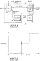
- FIG. 2 graphs system clock frequency (SYSTEM CLOCK) versus time during a start up period for the system in FIG. 1.
- SYSTEM CLOCK system clock frequency
- the system 100 is switching from a low power mode to an active mode and the reference clock is input into PLL 110.
- PLL 110 recognizes the reference clock and begins to acquire the target frequency. Because PLL 110 is initially operating in the wide bandwidth mode, a large overshoot in frequency occurs as PLL 100 rapidly attempts to acquire frequency lock to the reference clock, as can be seen in the graph of FIG. 2.
- Divider 130 divides the PLL clock by half to generate the system clock during this start-up mode but the CPU does not begin execution at this point.
- the FREQUENCY LOCK signal is output to counter 120, which initiates the 10 millisecond count based on the reference clock. The end of the count indicates when the PLL has sufficiently settled to transition to the narrow bandwidth operating mode.
- counter 120 outputs the PHASE LOCK signal to CPU 140 to enable CPU 140 to begin execution.
- PHASE LOCK is received by PLL 110 (connection not shown) to switch PLL 110 to narrow bandwidth operation.
- CPU 140 provides a X BIT to select the unity divisor of divider 130, which switches the SYSTEM CLOCK to the frequency of PLL CLOCK.
- CPU 140 is not allowed to execute code and therefore is not operational.
- clock generation circuit 100 and other circuits within the system have been switched from the low power mode into an active mode and are inefficiently consuming power.
- the present invention provides a method and system for reducing this inefficiency in systems having a low frequency reference clock by allowing the CPU to operate during the phase locking period at an useful operating frequency without allowing the system clock to exceed the system's maximum specified operating frequency.
- System 300 includes CPU 350 and CLOCK GENERATION CIRCUIT 305.
- a low frequency reference clock (REF) is input into dual bandwidth PLL 310 within circuit 305.
- PLL 310 operates in a wide bandwidth mode (highgain) when acquiring phaselock and a narrow bandwidth mode (lowgain) to maintain phaselock.
- PLL 310 synthesizes the reference clock to produce the PLL CLOCK as a function of a multiplication factor (N). In one embodiment, where the reference clock is a low frequency clock at 33 kilohertz, N is equal to 512.
- PLL 310 outputs the PLL CLOCK to a divider 330.
- Divider 330 is controlled by a SELECT signal output by AND gate 340 and is programmed to divide the PLL CLOCK to one of two desired operating frequencies as set by an input M as a SYSTEM CLOCK output.
- PLL 310 also outputs a FREQUENCY LOCK signal to a counter 320 and CPU 350.
- the FREQUENCY LOCK signal indicates when the PLL CLOCK has reached the programmed output frequency of the CLOCK GENERATION CIRCUIT to within a selected bandwidth. However, because the PLL must still reach a phase locked condition to allow the PLL to switch from the wide bandwidth to narrow bandwidth operation and reach a stable frequency, a settling period indicated by a PHASE LOCK signal is counted off by counter 320 to ensure that the PLL has phase-locked.
- the FREQUENCY LOCK signal initiates the target frequency enable counter 320 to count off the preset period from t 1 to t 2 .
- Counter 320 generates the PHASE LOCK signal input into AND gate 340 at the end of the count.
- the FREQUENCY LOCK signal also enables CPU 350 to begin operation and perform programmed tasks during the phase locking period. Because the processor is being clocked by SYSTEM CLOCK at a divided frequency, there is no danger of exceeding the maximum specified frequency during the phase/frequency lock period.
- CPU 350 can be programmed to assert the X BIT from a read/write register to request maximum speed operation at any desired time.
- the X BIT and the PHASE LOCK signal are input into AND gate 340.
- the SELECT output of AND gate 340 controls divider 330, where the SELECT signal selects the target frequency M to equal 1 or n.
- the SELECT signal selects the divider function of divider 330 as a selected divisor n until both the CPU 350 has requested full speed operation by asserting the X BIT and the settling period counted by counter 320 has expired.
- divider 330 switches to produce a SYSTEM CLOCK at the full frequency of the PLL CLOCK (or some fraction thereof as desired).
- FIG. 4 shows a graph of the system clock frequency (SYSTEM CLOCK) over time in one example of a start up period of the system of FIG. 3.
- the portable device 300 is switching from the low power mode to an active mode and the reference clock is input into PLL 310.
- PLL 310 recognizes the reference clock and begins to acquire the target frequency. Because PLL 310 is initially operating in the wide bandwidth mode, a large overshoot in frequency occurs as PLL 310 rapidly attempts to acquire frequency lock to the reference clock.
- Divider 330 divides the PLL clock by the divisor M to generate the system clock during this start-up mode.
- a FREQUENCY LOCK signal is output to counter 320, which begins to count a period (for example, a 10 millisecond period requiring 328 counts of counter 320) based on the reference clock.
- the FREQUENCY LOCK simultaneously enables CPU 350 to begin operation at around time t 1 , rather than t 2 as was seen in the prior art. This might allow a portable system such as a cellular phone to potentially complete the work required during that cellular cycle prior to the system reaching the maximum frequency operation at time t 2 . Because CPU 350 operates at half the maximum operating frequency while PLL 310 is phase locking, there is no danger of exceeding maximum frequency.
- counter 320 outputs the PHASE LOCK signal to AND gate 340, indicating the PLL has sufficiently settled to transition into narrow bandwidth phase. Also, PHASE LOCK is received by PLL 310 (connection not shown) to switch PLL 310 to narrow bandwidth operation.
- CPU 350 asserts the X BIT to select the unity divisor of divider 330, which switches the SYSTEM CLOCK to the frequency of PLL CLOCK. In a preferred embodiment, the frequency of PLL CLOCK would be the system's specified maximum frequency. As seen in FIG.
- the system of the present invention is able to achieve maximum operating frequency at time t 2 because CPU 350 has been executing at half frequency during the period t 1 -t 2 so that it is operational at the time phase lock occurs and can issue the X BIT immediately.
- the system of the preferred embodiment operates at half operating frequency during period t 1 -t 2 and full operating frequency between time t 2 and t 3 to allow the system to complete its operating tasks and return to low power mode sooner.
- the prior art system does not even begin to execute code until after t 3 .
- a PLL generates a PLL clock output to a divider, which divides the PLL clock to a system clock output.
- the PLL outputs a frequency lock signal upon acquiring a desired output frequency, which initiates a counter and enables execution in a CPU being clocked by the system clock.
- the CPU is thereby enabled to execute at a divided frequency during phase locking without risk of frequency overshoot induced failures.
- a select signal is produced that switches the divider to output a maximum frequency system clock, thereby enabling the CPU to execute at maximum frequency when the PLL is safely phase locked.
Landscapes
- Engineering & Computer Science (AREA)
- Theoretical Computer Science (AREA)
- Physics & Mathematics (AREA)
- General Engineering & Computer Science (AREA)
- General Physics & Mathematics (AREA)
- Stabilization Of Oscillater, Synchronisation, Frequency Synthesizers (AREA)
- Power Sources (AREA)
Applications Claiming Priority (2)
| Application Number | Priority Date | Filing Date | Title |
|---|---|---|---|
| US901645 | 1997-07-28 | ||
| US08/901,645 US5963068A (en) | 1997-07-28 | 1997-07-28 | Fast start-up processor clock generation method and system |
Publications (3)
| Publication Number | Publication Date |
|---|---|
| EP0895358A2 true EP0895358A2 (de) | 1999-02-03 |
| EP0895358A3 EP0895358A3 (de) | 1999-04-14 |
| EP0895358B1 EP0895358B1 (de) | 2003-09-03 |
Family
ID=25414580
Family Applications (1)
| Application Number | Title | Priority Date | Filing Date |
|---|---|---|---|
| EP98112947A Expired - Lifetime EP0895358B1 (de) | 1997-07-28 | 1998-07-13 | Verfahren und System zum Erzeugen eines Prozessortaktes mit schnellem Startvorgang |
Country Status (6)
| Country | Link |
|---|---|
| US (1) | US5963068A (de) |
| EP (1) | EP0895358B1 (de) |
| JP (1) | JP4206151B2 (de) |
| KR (1) | KR100546227B1 (de) |
| DE (1) | DE69817713T2 (de) |
| TW (1) | TW445404B (de) |
Cited By (2)
| Publication number | Priority date | Publication date | Assignee | Title |
|---|---|---|---|---|
| WO2003021407A1 (en) * | 2001-08-29 | 2003-03-13 | Analog Devices, Inc. | Phase locked loops fast power up methods and apparatus |
| EP1333580A1 (de) * | 1997-10-16 | 2003-08-06 | Oasis Silicon Systems Inc. | Vorrichtung mit einer Phasenregelschleife |
Families Citing this family (19)
| Publication number | Priority date | Publication date | Assignee | Title |
|---|---|---|---|---|
| US6763060B1 (en) * | 1999-02-19 | 2004-07-13 | Oasis Silicon Systems | Communication system employing a network of power managed transceivers that can generate a clocking signal or enable data bypass of a digital system associated with each transceiver |
| JP2000305655A (ja) * | 1999-04-19 | 2000-11-02 | Mitsubishi Electric Corp | 周波数逓倍回路内蔵のマイクロコンピュータ |
| JP4020548B2 (ja) * | 1999-11-11 | 2007-12-12 | 富士通株式会社 | フリップフロップ制御回路、プロセッサおよびプロセッサの動作方法 |
| US6859509B1 (en) * | 2000-02-04 | 2005-02-22 | The United States Of America As Represented By The Administrator Of The National Aeronautics And Space Administration | Wide bandwidth phase-locked loop circuit |
| KR100507880B1 (ko) * | 2000-05-31 | 2005-08-17 | 매그나칩 반도체 유한회사 | 개선된 위상고정루프 회로 |
| EP1289150A1 (de) * | 2001-08-24 | 2003-03-05 | STMicroelectronics S.r.l. | Verfahren zum Erzeugen eines Signals veränderbarer Frequenz, zum Beispiel zum Spreizen des Sprektrums eines Taktsignals, und Vorrichtung dafür |
| TW565758B (en) * | 2001-09-19 | 2003-12-11 | Alps Electric Co Ltd | Computer suppressing of unnecessary signals |
| US7036032B2 (en) * | 2002-01-04 | 2006-04-25 | Ati Technologies, Inc. | System for reduced power consumption by phase locked loop and method thereof |
| US7370189B2 (en) | 2004-09-30 | 2008-05-06 | Intel Corporation | Method and apparatus for establishing safe processor operating points in connection with a secure boot |
| GB2450564B (en) * | 2007-06-29 | 2011-03-02 | Imagination Tech Ltd | Clock frequency adjustment for semi-conductor devices |
| US9041452B2 (en) * | 2010-01-27 | 2015-05-26 | Silicon Laboratories Inc. | Circuit and method of clocking multiple digital circuits in multiple phases |
| JP2014090344A (ja) | 2012-10-31 | 2014-05-15 | Nec Corp | クロック信号初期化回路およびその方法 |
| JP6466740B2 (ja) * | 2015-03-02 | 2019-02-06 | 株式会社メガチップス | クロック生成回路 |
| KR102298160B1 (ko) * | 2015-08-13 | 2021-09-03 | 삼성전자주식회사 | 반도체 장치 및 이를 포함하는 통신 시스템 |
| KR102092126B1 (ko) | 2018-11-20 | 2020-03-23 | 배운성 | 이물질 감김 방지용 보트 스크류 보호장치 |
| FR3098665B1 (fr) * | 2019-07-09 | 2021-07-30 | St Microelectronics Rousset | Procédé de gestion du démarrage d’une boucle à verrouillage de phase, et circuit intégré correspondant |
| FR3112044B1 (fr) * | 2020-06-24 | 2023-10-27 | St Microelectronics Rousset | Procédé de gestion du démarrage d’une boucle à verrouillage de phase, et circuit intégré correspondant |
| CN113839666A (zh) * | 2020-06-24 | 2021-12-24 | 意法半导体(鲁塞)公司 | 用于管理锁相环的启动的处理和对应的集成电路 |
| US12040804B2 (en) * | 2022-04-28 | 2024-07-16 | Parade Technologies, Ltd. | Methods and systems for controlling frequency variation for a PLL reference clock |
Citations (7)
| Publication number | Priority date | Publication date | Assignee | Title |
|---|---|---|---|---|
| US4893271A (en) * | 1983-11-07 | 1990-01-09 | Motorola, Inc. | Synthesized clock microcomputer with power saving |
| EP0385567A2 (de) * | 1989-02-28 | 1990-09-05 | International Business Machines Corporation | Taktsignalgenerator für ein Datenverarbeitungssystem |
| US5579353A (en) * | 1993-10-12 | 1996-11-26 | Texas Instruments Incorporated | Dynamic clock mode switch |
| US5606293A (en) * | 1994-12-14 | 1997-02-25 | Mitsubishi Denki Kabushiki Kaisha | Clock generator for microcomputer having reduced start-up time |
| EP0766404A2 (de) * | 1995-09-28 | 1997-04-02 | Nec Corporation | Taktgenerator mit einer Phasenregelkreisschaltung |
| US5623234A (en) * | 1996-03-04 | 1997-04-22 | Motorola | Clock system |
| US5774701A (en) * | 1995-07-10 | 1998-06-30 | Hitachi, Ltd. | Microprocessor operating at high and low clok frequencies |
Family Cites Families (4)
| Publication number | Priority date | Publication date | Assignee | Title |
|---|---|---|---|---|
| US4758945A (en) * | 1979-08-09 | 1988-07-19 | Motorola, Inc. | Method for reducing power consumed by a static microprocessor |
| US4748559A (en) * | 1979-08-09 | 1988-05-31 | Motorola, Inc. | Apparatus for reducing power consumed by a static microprocessor |
| JPH06253568A (ja) * | 1993-03-03 | 1994-09-09 | Sony Corp | 基準信号発生装置 |
| US5694308A (en) * | 1995-07-03 | 1997-12-02 | Motorola, Inc. | Method and apparatus for regulated low voltage charge pump |
-
1997
- 1997-07-28 US US08/901,645 patent/US5963068A/en not_active Expired - Lifetime
-
1998
- 1998-06-26 TW TW087110385A patent/TW445404B/zh not_active IP Right Cessation
- 1998-07-10 JP JP21197598A patent/JP4206151B2/ja not_active Expired - Fee Related
- 1998-07-13 EP EP98112947A patent/EP0895358B1/de not_active Expired - Lifetime
- 1998-07-13 DE DE69817713T patent/DE69817713T2/de not_active Expired - Fee Related
- 1998-07-28 KR KR1019980030256A patent/KR100546227B1/ko not_active IP Right Cessation
Patent Citations (7)
| Publication number | Priority date | Publication date | Assignee | Title |
|---|---|---|---|---|
| US4893271A (en) * | 1983-11-07 | 1990-01-09 | Motorola, Inc. | Synthesized clock microcomputer with power saving |
| EP0385567A2 (de) * | 1989-02-28 | 1990-09-05 | International Business Machines Corporation | Taktsignalgenerator für ein Datenverarbeitungssystem |
| US5579353A (en) * | 1993-10-12 | 1996-11-26 | Texas Instruments Incorporated | Dynamic clock mode switch |
| US5606293A (en) * | 1994-12-14 | 1997-02-25 | Mitsubishi Denki Kabushiki Kaisha | Clock generator for microcomputer having reduced start-up time |
| US5774701A (en) * | 1995-07-10 | 1998-06-30 | Hitachi, Ltd. | Microprocessor operating at high and low clok frequencies |
| EP0766404A2 (de) * | 1995-09-28 | 1997-04-02 | Nec Corporation | Taktgenerator mit einer Phasenregelkreisschaltung |
| US5623234A (en) * | 1996-03-04 | 1997-04-22 | Motorola | Clock system |
Cited By (5)
| Publication number | Priority date | Publication date | Assignee | Title |
|---|---|---|---|---|
| EP1333580A1 (de) * | 1997-10-16 | 2003-08-06 | Oasis Silicon Systems Inc. | Vorrichtung mit einer Phasenregelschleife |
| WO2003021407A1 (en) * | 2001-08-29 | 2003-03-13 | Analog Devices, Inc. | Phase locked loops fast power up methods and apparatus |
| US6768358B2 (en) | 2001-08-29 | 2004-07-27 | Analog Devices, Inc. | Phase locked loop fast power up methods and apparatus |
| US6889331B2 (en) | 2001-08-29 | 2005-05-03 | Analog Devices, Inc. | Dynamic voltage control method and apparatus |
| CN100451914C (zh) * | 2001-08-29 | 2009-01-14 | 联发科技股份有限公司 | 锁相环迅速加电方法和装置 |
Also Published As
| Publication number | Publication date |
|---|---|
| DE69817713T2 (de) | 2004-04-08 |
| KR19990014219A (ko) | 1999-02-25 |
| US5963068A (en) | 1999-10-05 |
| JP4206151B2 (ja) | 2009-01-07 |
| JPH11234125A (ja) | 1999-08-27 |
| EP0895358B1 (de) | 2003-09-03 |
| DE69817713D1 (de) | 2003-10-09 |
| TW445404B (en) | 2001-07-11 |
| EP0895358A3 (de) | 1999-04-14 |
| KR100546227B1 (ko) | 2006-03-28 |
Similar Documents
| Publication | Publication Date | Title |
|---|---|---|
| US5963068A (en) | Fast start-up processor clock generation method and system | |
| JP5159316B2 (ja) | オンデマンド電力管理の方法及び機器 | |
| JP4243186B2 (ja) | 位相ロックループの高速起動方法および装置 | |
| US5964881A (en) | System and method to control microprocessor startup to reduce power supply bulk capacitance needs | |
| US7434083B1 (en) | Method and apparatus for the generation and control of clock signals | |
| US6366157B1 (en) | Methods and circuits for dynamically adjusting a supply voltage and/or a frequency of a clock signal in a digital circuit | |
| US7622996B2 (en) | Multi-loop phase locked loop circuit | |
| US6879188B2 (en) | Semiconductor integrated circuit device | |
| EP0840196A2 (de) | Schaltungsanordnung zur Umschaltung zwischen Taktquellen in einem Datenverarbeitungssystem | |
| JP2008524744A (ja) | オンデマンド電力管理の方法及び機器 | |
| EP0840195A2 (de) | Anordnung und Verfahren zur Taktsequenzierung in einem Datenverarbeitungssystem | |
| JP2001051747A (ja) | クロック制御回路 | |
| US6255882B1 (en) | Method and system of switching clock signal | |
| US6211739B1 (en) | Microprocessor controlled frequency lock loop for use with an external periodic signal | |
| EP1688820A2 (de) | Taktversorgungsverfahren und Informationsverarbeitungsvorrichtung | |
| US8760202B1 (en) | System for generating clock signal | |
| US7496774B2 (en) | Method and system for generating clocks for standby mode operation in a mobile communication device | |
| KR19990006825A (ko) | 무선 휴대 단말기 | |
| US8402288B2 (en) | Apparatus and method for controlling voltage and frequency using multiple reference circuits | |
| US7813410B1 (en) | Initiating spread spectrum modulation | |
| KR100334777B1 (ko) | 이동통신 단말기의 주파수 합성부 | |
| JP2003347931A (ja) | Pllを搭載した半導体集積回路 | |
| JP2004056363A (ja) | 暗号処理装置及び電力平準化制御方法 |
Legal Events
| Date | Code | Title | Description |
|---|---|---|---|
| PUAI | Public reference made under article 153(3) epc to a published international application that has entered the european phase |
Free format text: ORIGINAL CODE: 0009012 |
|
| AK | Designated contracting states |
Kind code of ref document: A2 Designated state(s): DE FR GB IT NL |
|
| AX | Request for extension of the european patent |
Free format text: AL;LT;LV;MK;RO;SI |
|
| PUAL | Search report despatched |
Free format text: ORIGINAL CODE: 0009013 |
|
| AK | Designated contracting states |
Kind code of ref document: A3 Designated state(s): AT BE CH CY DE DK ES FI FR GB GR IE IT LI LU MC NL PT SE |
|
| AX | Request for extension of the european patent |
Free format text: AL;LT;LV;MK;RO;SI |
|
| 17P | Request for examination filed |
Effective date: 19991014 |
|
| AKX | Designation fees paid |
Free format text: DE FR GB IT NL |
|
| 17Q | First examination report despatched |
Effective date: 20020131 |
|
| GRAH | Despatch of communication of intention to grant a patent |
Free format text: ORIGINAL CODE: EPIDOS IGRA |
|
| GRAH | Despatch of communication of intention to grant a patent |
Free format text: ORIGINAL CODE: EPIDOS IGRA |
|
| GRAA | (expected) grant |
Free format text: ORIGINAL CODE: 0009210 |
|
| AK | Designated contracting states |
Kind code of ref document: B1 Designated state(s): DE FR GB IT NL |
|
| REG | Reference to a national code |
Ref country code: GB Ref legal event code: FG4D |
|
| REF | Corresponds to: |
Ref document number: 69817713 Country of ref document: DE Date of ref document: 20031009 Kind code of ref document: P |
|
| ET | Fr: translation filed | ||
| PLBE | No opposition filed within time limit |
Free format text: ORIGINAL CODE: 0009261 |
|
| STAA | Information on the status of an ep patent application or granted ep patent |
Free format text: STATUS: NO OPPOSITION FILED WITHIN TIME LIMIT |
|
| 26N | No opposition filed |
Effective date: 20040604 |
|
| REG | Reference to a national code |
Ref country code: GB Ref legal event code: 732E |
|
| NLS | Nl: assignments of ep-patents |
Owner name: FREESCALE SEMICONDUCTOR, INC. Effective date: 20051028 |
|
| PGFP | Annual fee paid to national office [announced via postgrant information from national office to epo] |
Ref country code: GB Payment date: 20060614 Year of fee payment: 9 |
|
| PGFP | Annual fee paid to national office [announced via postgrant information from national office to epo] |
Ref country code: NL Payment date: 20060616 Year of fee payment: 9 |
|
| PGFP | Annual fee paid to national office [announced via postgrant information from national office to epo] |
Ref country code: FR Payment date: 20060705 Year of fee payment: 9 |
|
| PGFP | Annual fee paid to national office [announced via postgrant information from national office to epo] |
Ref country code: IT Payment date: 20060731 Year of fee payment: 9 Ref country code: DE Payment date: 20060731 Year of fee payment: 9 |
|
| GBPC | Gb: european patent ceased through non-payment of renewal fee |
Effective date: 20070713 |
|
| NLV4 | Nl: lapsed or anulled due to non-payment of the annual fee |
Effective date: 20080201 |
|
| PG25 | Lapsed in a contracting state [announced via postgrant information from national office to epo] |
Ref country code: NL Free format text: LAPSE BECAUSE OF NON-PAYMENT OF DUE FEES Effective date: 20080201 Ref country code: DE Free format text: LAPSE BECAUSE OF NON-PAYMENT OF DUE FEES Effective date: 20080201 |
|
| PG25 | Lapsed in a contracting state [announced via postgrant information from national office to epo] |
Ref country code: GB Free format text: LAPSE BECAUSE OF NON-PAYMENT OF DUE FEES Effective date: 20070713 |
|
| REG | Reference to a national code |
Ref country code: FR Ref legal event code: ST Effective date: 20080331 |
|
| PG25 | Lapsed in a contracting state [announced via postgrant information from national office to epo] |
Ref country code: FR Free format text: LAPSE BECAUSE OF NON-PAYMENT OF DUE FEES Effective date: 20070731 |
|
| PG25 | Lapsed in a contracting state [announced via postgrant information from national office to epo] |
Ref country code: IT Free format text: LAPSE BECAUSE OF NON-PAYMENT OF DUE FEES Effective date: 20070713 |