EP0758182A2 - Festkörperbildaufnahmevorrichtung - Google Patents
Festkörperbildaufnahmevorrichtung Download PDFInfo
- Publication number
- EP0758182A2 EP0758182A2 EP96401514A EP96401514A EP0758182A2 EP 0758182 A2 EP0758182 A2 EP 0758182A2 EP 96401514 A EP96401514 A EP 96401514A EP 96401514 A EP96401514 A EP 96401514A EP 0758182 A2 EP0758182 A2 EP 0758182A2
- Authority
- EP
- European Patent Office
- Prior art keywords
- signal
- unit
- solid state
- image sensing
- clamp
- Prior art date
- Legal status (The legal status is an assumption and is not a legal conclusion. Google has not performed a legal analysis and makes no representation as to the accuracy of the status listed.)
- Withdrawn
Links
Images



Classifications
-
- H—ELECTRICITY
- H04—ELECTRIC COMMUNICATION TECHNIQUE
- H04N—PICTORIAL COMMUNICATION, e.g. TELEVISION
- H04N25/00—Circuitry of solid-state image sensors [SSIS]; Control thereof
- H04N25/70—SSIS architectures; Circuits associated therewith
- H04N25/701—Line sensors
-
- H—ELECTRICITY
- H04—ELECTRIC COMMUNICATION TECHNIQUE
- H04N—PICTORIAL COMMUNICATION, e.g. TELEVISION
- H04N25/00—Circuitry of solid-state image sensors [SSIS]; Control thereof
- H04N25/60—Noise processing, e.g. detecting, correcting, reducing or removing noise
- H04N25/63—Noise processing, e.g. detecting, correcting, reducing or removing noise applied to dark current
- H04N25/633—Noise processing, e.g. detecting, correcting, reducing or removing noise applied to dark current by using optical black pixels
-
- H—ELECTRICITY
- H04—ELECTRIC COMMUNICATION TECHNIQUE
- H04N—PICTORIAL COMMUNICATION, e.g. TELEVISION
- H04N25/00—Circuitry of solid-state image sensors [SSIS]; Control thereof
- H04N25/60—Noise processing, e.g. detecting, correcting, reducing or removing noise
- H04N25/67—Noise processing, e.g. detecting, correcting, reducing or removing noise applied to fixed-pattern noise, e.g. non-uniformity of response
- H04N25/671—Noise processing, e.g. detecting, correcting, reducing or removing noise applied to fixed-pattern noise, e.g. non-uniformity of response for non-uniformity detection or correction
-
- H—ELECTRICITY
- H04—ELECTRIC COMMUNICATION TECHNIQUE
- H04N—PICTORIAL COMMUNICATION, e.g. TELEVISION
- H04N25/00—Circuitry of solid-state image sensors [SSIS]; Control thereof
- H04N25/60—Noise processing, e.g. detecting, correcting, reducing or removing noise
- H04N25/67—Noise processing, e.g. detecting, correcting, reducing or removing noise applied to fixed-pattern noise, e.g. non-uniformity of response
- H04N25/671—Noise processing, e.g. detecting, correcting, reducing or removing noise applied to fixed-pattern noise, e.g. non-uniformity of response for non-uniformity detection or correction
- H04N25/673—Noise processing, e.g. detecting, correcting, reducing or removing noise applied to fixed-pattern noise, e.g. non-uniformity of response for non-uniformity detection or correction by using reference sources
-
- H—ELECTRICITY
- H04—ELECTRIC COMMUNICATION TECHNIQUE
- H04N—PICTORIAL COMMUNICATION, e.g. TELEVISION
- H04N25/00—Circuitry of solid-state image sensors [SSIS]; Control thereof
- H04N25/70—SSIS architectures; Circuits associated therewith
- H04N25/71—Charge-coupled device [CCD] sensors; Charge-transfer registers specially adapted for CCD sensors
-
- H—ELECTRICITY
- H04—ELECTRIC COMMUNICATION TECHNIQUE
- H04N—PICTORIAL COMMUNICATION, e.g. TELEVISION
- H04N25/00—Circuitry of solid-state image sensors [SSIS]; Control thereof
- H04N25/70—SSIS architectures; Circuits associated therewith
- H04N25/71—Charge-coupled device [CCD] sensors; Charge-transfer registers specially adapted for CCD sensors
- H04N25/713—Transfer or readout registers; Split readout registers or multiple readout registers
-
- H—ELECTRICITY
- H04—ELECTRIC COMMUNICATION TECHNIQUE
- H04N—PICTORIAL COMMUNICATION, e.g. TELEVISION
- H04N25/00—Circuitry of solid-state image sensors [SSIS]; Control thereof
- H04N25/70—SSIS architectures; Circuits associated therewith
- H04N25/71—Charge-coupled device [CCD] sensors; Charge-transfer registers specially adapted for CCD sensors
- H04N25/74—Circuitry for scanning or addressing the pixel array
-
- H—ELECTRICITY
- H04—ELECTRIC COMMUNICATION TECHNIQUE
- H04N—PICTORIAL COMMUNICATION, e.g. TELEVISION
- H04N25/00—Circuitry of solid-state image sensors [SSIS]; Control thereof
- H04N25/70—SSIS architectures; Circuits associated therewith
- H04N25/71—Charge-coupled device [CCD] sensors; Charge-transfer registers specially adapted for CCD sensors
- H04N25/745—Circuitry for generating timing or clock signals
-
- H—ELECTRICITY
- H04—ELECTRIC COMMUNICATION TECHNIQUE
- H04N—PICTORIAL COMMUNICATION, e.g. TELEVISION
- H04N25/00—Circuitry of solid-state image sensors [SSIS]; Control thereof
- H04N25/70—SSIS architectures; Circuits associated therewith
- H04N25/71—Charge-coupled device [CCD] sensors; Charge-transfer registers specially adapted for CCD sensors
- H04N25/75—Circuitry for providing, modifying or processing image signals from the pixel array
-
- H—ELECTRICITY
- H04—ELECTRIC COMMUNICATION TECHNIQUE
- H04N—PICTORIAL COMMUNICATION, e.g. TELEVISION
- H04N25/00—Circuitry of solid-state image sensors [SSIS]; Control thereof
- H04N25/70—SSIS architectures; Circuits associated therewith
- H04N25/76—Addressed sensors, e.g. MOS or CMOS sensors
-
- H—ELECTRICITY
- H04—ELECTRIC COMMUNICATION TECHNIQUE
- H04N—PICTORIAL COMMUNICATION, e.g. TELEVISION
- H04N25/00—Circuitry of solid-state image sensors [SSIS]; Control thereof
- H04N25/70—SSIS architectures; Circuits associated therewith
- H04N25/76—Addressed sensors, e.g. MOS or CMOS sensors
- H04N25/78—Readout circuits for addressed sensors, e.g. output amplifiers or A/D converters
Definitions
- the present invention relates to a solid-state image sensing device employing solid-state image sensing elements which serve as area or linear sensors.
- the present invention relates to a solid-state image sensing device which clamps a signal output by a solid-state image sensing element thereof to a predetermined reference potential.
- a solid-state image sensing device employing CCD solid-state image sensing elements such as CCD linear sensors as shown in Fig. 1, differential operations are carried out at a signal processing unit 15 at a later stage by clamping a black level or holding samples in order to compensate for an offset due to the optical transmission through a CCD shift register (serving as an electric-charge transferring unit) 13 for transferring signal electric charge read out from a sensor array 11 and to cancel dark-current components.
- a CCD shift register serving as an electric-charge transferring unit 13 for transferring signal electric charge read out from a sensor array 11 and to cancel dark-current components.
- FIG. 2 An actual circuit configuration of the signal processing unit 15 is shown in Fig. 2.
- the black level the level of picture element signals at shading unit 11a and 11b which are also referred to as optical black (OPB) units at the sensor array 11 is meant.
- OPB optical black
- the shading units 11a and 11b are also referred to hereafter as a second OPE unit and a first OPB unit respectively.
- a signal output Vout In order to process digitally a signal output Vout, and A/D converter 16 is provided at a later stage of the signal processing unit 15.
- the signal output Vout a clamped output of a clamp circuit 22 is converted into a digital signal by the A/D converter 16.
- Vref the reference potential of the A/D converter 16
- the reference potential Vref of the A/D converter 16 is set at the maximum level of the input D range.
- the signal output by the empty transmission unit 13a of the CCD shift register 13 can also be clamped to the reference potential Vref of the A/D converter 16.
- the D range of the A/D converter 16 that can be used for the signal becomes narrower by the dark-current portion.
- the level of the image sensing picture element signal is also shifted by a displacement determined by the dark-current portion.
- signal processing for subtracting the dark-current portion and the like is required, inevitably making the circuit configuration accordingly complicated.
- a solid-state image sensing device is disclosed in Japanese Patent Laid-open No. Hei 7-30820 with a configuration wherein a timing generator 17 generates clamp pulses ⁇ CLP1 and ⁇ CLP2 for clamping the signals of the empty transmission unit 13a of the CCD shift register 13 and the OPB unit 11b on the rear side of the sensor array 11 respectively each over a period of time corresponding to one picture element as shown in timing charts of Fig. 22.
- the clamp pulse ⁇ CLP1 is set with clamp timing for a signal portion of a signal output by the empty transmission unit 13a of the CCD shift register 13 corresponding to the 1st picture element while the clamp pulse ⁇ CLP2 is set with clamp timing for a portion of a signal output by the OPB unit 11b on the rear side of the sensor array 11 corresponding to the 2nd picture element or a subsequent one.
- the A/D conversion is carried out by the A/D converter 16 on a later stage with timing not to sample a portion of a signal output by the empty transmission unit 13a of the CCD shift register 13 corresponding to 1st picture element.
- notation ⁇ ROG shown in timing charts of Fig. 22 denotes a read gate pulse which is applied to a shift gate 12 for reading out signal electric charge from the sensor array 11.
- Notations ⁇ H1 and ⁇ H2 are transfer clocks of the CCD shift register 13 whereas notation ⁇ RS is a reset pulse for resetting an electric-charge detecting unit 14.
- Rotation ⁇ SH is a semple/hold pulse for a sample/hold circuit 21 of a signal processing unit 15.
- Notation Va is a sample/hold signal output by the sample/hold circuit 21 whereas notation ⁇ CLP (strictly speaking, notations ⁇ CLP1 and ⁇ CLP2) are clamp pulses of a clamp circuit 22.
- Notation Vout denotes a signal output.
- the operation to clamp a portion of a signal output by the empty transmission unit 13a corresponding to the first picture element using the clamp pulse ⁇ CLP1 prevents a signal voltage higher than the reference potential Vref of the A/D convecter 16 from being supplied to the A/D converter 16 only during a minimum unit time of the empty transmission period.
- the A/D converter 16 does not sample a portion of a signal output by the empty transmission unit 13a corresponding to the first picture element. As a result, a signal voltage higher than the reference potential Vref of the A/D converter 16 is not supplied to the A/D converter 16.
- the sampling time of the A/D converter 16 must be set so that a portion of a signal output by the empty transmission unit 13a corresponding to the first picture element is not sampled, giving rise to a difficulty that it is necessary to modify the sampling time of the A/D converter which is implemented by an externally attached circuit.
- the A/D converter 16 will not function correctly and data resulting from the A/D conversion is therefore incorrect.
- the A/D converter 16 itself could be damaged in an extreme case.
- the present invention addresses the problems described above. It is an object of the present invention to provide a solid-state image sensing device wherein a signal output by a solid-state image sensing element employed thereby is clamped to a predetermined reference potential so as to eliminate an adverse effect on an A/D converted at a later stage.
- a timing generator employed in a solid-state image sensing device has a configuration wherein clamp pulses are generated for clamping portion corresponding to at least one picture element of an OPB unit on the rear side in a signal output by a solid-state image sensing element and for clamping a signal output by an empty transmission unit of an electric-charge transferring unit over a period of time covering an inhibit period of transfer clocks.
- a timing generator employed in a solid-state image sensing device has a configuration wherein clamp pulse are generated for clamping a signal a portion corresponding to at least one picture element of an OPB unit on the rear side in a signal output by a solid-state image sensing element and for clamping a signal over a period of time between a halfway point of time in a signal output by an OPB unit on the front side and a halfway point of time in a signal output by an empty transmission unit of an electric-charge transferring unit.
- a timing generator employed in a solid-state image sensing device has a configuration wherein clamp pulses are generated for clamping a signal portion corresponding to at least one picture element of an OPB unit on the rear side in a signal output by a solid-state image sensing element and for clamping a signal over a period of time between a halfway point of time in a signal output by an OPB unit on the front side and the end of an inhibit period of transfer clocks for a signal output by an empty transmission unit of an electric-charge transferring unit.
- a timing generator employed in a solid-state image sensing device has a configuration wherein clamp pulses are generated for clamping a signal portion corresponding to at least one picture element of an OPB unit on the rear side in a signal output by a solid-state image sensing elememt and for clamping a signal over a period of time between a halfway point of time in a signal of the last picture element preceding ahead by one line and the end of an inhibit period of transfer clocks for a signal output by an empty transmission unit of an electric-charge transferring unit.
- a timing generator employed in a solid-state image sensing device to a fifth feature of the invention has a configuration wherein a clamp pulse is generating for clamping at least a picture element signal not superpositioned on a picture element signal obtained from a previous read operation in the case where an operation to read signal electric charge occurs during a transfer period of signal electric charge.
- a timing generator employed in a solid-state image sensing device has a configuration including an inhibit circuit for inhibiting generation of clamp pulses in synchronization with an operation to read out signal electric charge during a transfer period of signal electric charge in the case where such a read operation occurs.
- a signal portion output by the OPB unit on the rear aide in a signal output by the solid-state image element is clamped so as to detect a signal level of the OPB unit which level serves as a referen ce of level detection of a dark current and the like.
- a high signal voltage generated in company with transfer suspension caused by the inhibition of the transfer clocks can be masked out so that the high signal voltage is not supplied to an A/D converter at a later stage.
- a signal portion output by the OPB unit on the rear side in a signal outout by the solid-state image sensing element is clamped so as to detect a signal level of the OPB unit which level serves as a reference of level detection of a dark current and the like.
- a signal voltage higher than a reference voltage which signal voltage accompanies a dark current and the like is not generated at all over the entire empty transmission portion.
- the solid-state image sensing device by clamping a signal over a period of time between a halfway point of time in a signal output by an OPB unit on the front side and the end of an inhibit period of transfer clocks for a signal output by an empty transmission unit of an electric-charge transferring unit, in addition to the fact that a signal voltage higher than a reference voltage which signal voltage accompanies a dark current and the like is not generated at all over the entire empty transmission portion, a high signal voltage generated in company with transfer suspension caused by the inhibition of the transfer clocks can also be masked out.
- the signal output by an OPB unit on the rear side in a signal output by the solid-state image sensing element is clamped so as to detect a signal level of the OPB unit which level serves as a reference of level detection of a dark current and the like.
- the solid-state image sensing device when an operation to read out electric charge is carried out in a transfer period of signal electric charge, by clamping at least a picture signal not superpositioned on a picture element signal output by a previous read operation, the signal voltages of the image sensing picture element signal portion with no residual signal, the OPB unit and the empty transmission unit can be suppressed to a level below the reference voltage.
- a reset is applied in the course of transferring signal electric charge so that the signal voltage of the image sensing picture element signal portion with no residual signal, the OPB unit and the empty transmission unit will never exceed the reference voltage even if a newly read out signal is superpositioned on a residual signal being transferred in the electric-charge transferring unit.
- the solid-state image sensing device when an operation to read out electric charge is carried out in a transfer period of signal electric charge, by inhibiting the generation of clamp pulses in synchronization with the operation to read out electric charge, a reset is applied in the course of transferring signal electric charge so that, even if a newly read out signal is superpositioned on a residual signal being transferred in the electric-charge transferring unit, causing the picture element signals of them OPB units to increase in magnitude by the residual signal portion, the clamping of signals output by the OPB units is not carried out.
- the signal voltages of the image sensing picture element signal portion with no residual signal, the OPB unit and the empty transmission unit can be suppressed to a level below the reference voltage.
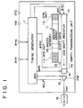
- Fig. 1 is a configuration diagram showing a typical solid-state image sensing device provided by the present invention which device employs, typically, linear sensors.
- the configuration includes a sensor array or a sensor unit 11 comprising a plurality of photosensors PS which are arranged to form a one-dimensional array.
- Each of the photosensors is used for carrying out opto-electric conversion, whereby incident light is converted into a signal electric charge having an amount proportional to the quantity of the light, and for accumulating the signal electric charge.
- OPB units 11a and 11b are provided at the front and rear ends of the sensor array 11 in the time-axis direction respectively.
- each of the OPB units 11a and 11b a plurality of picture elements are shaded.
- the signal electric charge accumulated in the sensor array 11 in picture element units is read out and transferred to a CCD shift register (an electric-charge transferring unit) 13 through a shift gate 12.
- the read out signal electric charge is transferred sequentially by the CCD shift register 13 and supplied to an electric-charge detecting unit 14.
- the CCD shift register 13 includes an empty transmission unit 13a only for empty transmission of signal electric charge in addition to transfer regions associated with picture elements of the sensor unit 11.
- the empty transmission unit 13a is provided at the end of the CCD shift register 13 close to the electric-charge detecting unit 14.
- the electric-charge detecting unit 14 detects signal electric charge transferred by the CCD shift register 13 and injected into an FD unit of the electric-charge detecting unit 14 and converts the signal eletric charge into a signal voltage to be supplied to a signal processing unit is at a later stage.
- the signal processing unit 15 comprises a sample/hold circuit 21 and a clamp circuit 22.
- the sample/hold circuit 21 is used for sampling and holding a signal voltage supplied by the electric-charge detecting unit 14 through a buffer 23.
- the clamp circuit 22 is used for clamping a sample/hold output supplied by the sample-hold circuit 21 through a buffer 24 and an alternating-current coupling condenser C and for supplying a signal Vout at a clamped level to an A/D converter 16 through a buffer 25.
- the signal processing unit 15 is created on the same substrate as the CCD chip.
- the clamp level of the clamp circuit 22 is set at a reference level Vref of the A/D converter 16.
- the clamp circuit 22 is placed at the later stage of the sample/hold circuit 21 and has a circuit configuration which clamps a sample/hold output. It should be noted that it is possible to place the clamp circuit 22 at the front stage of the sample/hold circuit 21. In this case, the clamp circuit 22 has a circuit configuration for clamping a detection signal output by the electric-charge detecting unit 14.
- timing generator 17 for generating a variety of timing signals is also created on the same substrat as the CCD chip.
- the timing generator 17 generates:
- the generation of the signals described above is based on the read gate signal ⁇ ROG and a master clock signal ⁇ clk supplied by an external source.
- the timing generator 17 also generates a final clamp pulse signal ⁇ CLP based on the read gate pulse signal ⁇ ROG and the transfer clock signal ⁇ H1.
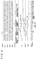
- the timing with which the clamp pulses ⁇ CLP are generated by the timing generator 17 is a characterizing feature offered by the present invention. Characterizing features of a 1st embodiment provided by the present invention are explained by referring to timing charts shown in Fig. 3, as follows. It should be noted that the timing charts shown in Fig. 3 are typical timing charts showing a picture element sequence in a unit cycle which comprises three picture elements of the empty transmission unit 13a, four picture elements of the first OPB unit 11b, typically 2,048 image sensing picture elements, two picture elements of the second OPB unit 11a and three picture elements of the transmission unit 13a if the picture element sequence is seen to start from the falling edge of the read pulse ⁇ ROG.
- timing charts of Fig. 3 also show the sample/hold signal Va output by the sample/hold circuit 21, the clamped signal Vout output by the clamp circuit 22 and A/D timing pulses of the A/D converter 16 besides the various timing signals ⁇ ROG, ⁇ H1, ⁇ H2, ⁇ RS, ⁇ SH, ⁇ CLPO and ⁇ CLP described above.
- the timing generator 17 employed in the 1st embodiment generates not only the clamp pulses ⁇ CLP2 for clamping a signal output by the first OPB unit 11b, one of signals output by the linear sensors, but also the clamp pulses ⁇ CLP1 also for clamping a signal output by the empty transmission unit 13a of the CCD shift register 13.
- the clamp pulses ⁇ CLP1 are generated with timing for clamping the signal output by the empty transmission unit 13a of the CCD shift register 13 over a period of time covering an inhibit period of the transfer clocks ⁇ H1 and ⁇ H2.
- the clamp pulses ⁇ CLP2 are generated with a timing for clamping a portion of the signal output by the first OPB unit 11b which portion includes the second picture element or a subsequent one.
- Fig. 4 is a block diagram showing a typical clamp-pulse generating circuit embedded in the timing generator 17 as is implemented by the first embodiment.
- the clamp-pulse generating circuit comprises an 11-bit counter 41, a JK flip-flop 42, a shift register 43, an AND circuit 44 and an OR circuit 45.
- the 11-bit counter 41 receives the read gate pulse ⁇ ROG as a CL (clear) input
- the 11-bit counter 41 counts the number of transfer clocks ⁇ H1 supplied thereto.
- the JK flip-flop 42 receives a signal V1 output by the 11-bit counter 41 as a J input and the road gate pulse ⁇ ROG as a K input.
- the shift register 43 supplies a 2-bit delay output and an 11-bit delay output to the AND circuit 44.
- the OR circuit 45 receives a signal output by the AND circuit 44 and the clamp pulse signal ⁇ CLPO. Details of the 11-bit counter 41 are shown in Fig. 5. As shown in the figure, the 11-bit counter 41 comprises eleven T flip-flop 50 1 to 50 11 which are connected to each other.
- notations V1 and V2 shown in Fig. 6 denote the signals output by the 11-bit counter 41 and the Q output of the JK flip-flop 42 respectively.
- the 11-bit counter 41 shown in Fig. 4 is cleared by the read gate pulse ⁇ ROG Every time a transfer clock ⁇ H1 is counted by the 11-bit counter 41, the polarity of the output V1 thereof is inverted.
- the JK flip-flop 42 is set with a timing determined by the rising edge of the output V1 of the 11-bit counter 41 to an "H" level and reset by the read gate pulse ⁇ ROG supplied thereto. As a result, the Q output of the JK flip-flop 42 is sustained at an "H" level over a period of time between the rising edge of the output V1 after a reset and the next reset.
- the Q output V2 of the JK flip-flop 42 is delayed by the shift register 43 by 2 bits and then further delayed by 11 bits.
- the two delayed outputs of the shift register 43 are supplied to the AND circuit 44 for producing a logical product of the two delayed outputs.
- the logical product produced by the AND circuit 44 and a clamp pulse ⁇ CLPO are supplied to the OR circuit 45 for producing a logical sum thereof which sum serves as a clamp pulse ⁇ CLP comprising the clamp pulses ⁇ CLP1 and ⁇ CLP2 described above.
- the clamp pulse signal ⁇ CLP is supplied to the clamp circuit 22 shown in Fig. 2.
- the clamp circuit 22 clamps the sample/hold output Va for the empty transmission unit 13a to the clamp level Vref over a period of time covering an inhibit period of the transfer clocks ⁇ H1 and ⁇ H2.
- the clamp circuit 22 clamps the sample/hold output Va to the clamp level Vref for the 2nd picture element or a subsequent first OPB unit 11b.
- the sample/hold output Va of the first OPB unit 11b is clamped to the clamp level Wref, but the sample/hold output Va for the empty transmission unit 13a is also clamped to the clamp level Vref over a period of time covering an inhibit period of the transfer clocks ⁇ H1 and ⁇ H2.
- the high signal voltage (a) is clamped in response to the clamp pulse ⁇ CLP1 to mask out the excessive portion, preventing the high signal voltage (a) from being supplied as it is to the A/D converter 16.
- the sample/hold output Va for the second picture element or a subsequent first OPB unit 11b can be detected.
- the level of a dark component such as a dark current and the like can be dectected from the sample/hold output Va for the first picture element.
- the high signal voltage (a) accompanying transfer suspension can be prevented from being supplied to the A/D converter 16. It should be noted, however, that a signal voltage (b) higher than the reference signal Vref accompanying a dark component and the like observed in the empty transmission unit 13a prior to the transfer suspension is input to the A/D converter 16. Nonetheless, the high signal voltage (a) accompanying transfer suspension has a potential higher than the signal voltage (b) accompanying a dark current and the like.
- a second embodiment provided by the present invention is explained by referring to timing charts shown in Fig. 7. It should be noted that a picture element sequence shown in Fig. 7 is the same as the one shown in Fig. 3.
- the timing generator 17 generates clock signals for clamping some of the signals output by the linear sensors.
- the timing generator 17 generates the clamp pulse signal ⁇ CLP2 for clamping a signal output by the first OPB unit 11b and the clamp pulse signal ⁇ CLP1 for clamping not only a signal output by the empty transmission unit 13a but also a signal output by the second OPB unit 11a.
- the clamp pulses ⁇ CLP1 are generated for clamping the signals over a period of time between a halfway point of time in a signal output by the second OPB unit 11a and the end of an inhibit period of transfer clocks ⁇ H1 and ⁇ H2 for a signal output by the empty transmission unit 13a of the CCD shift register 13.
- the clamp pulse signal ⁇ CLP2 is generated with timing to clamp a portion of a signal output by the first OPB unit 11b which portion represents the second picture element or a subsequent one.
- Fig. 8 is a block diagram showing a typical clamp-pulse generating circuit embedded in the timing generator 17 as implemented by the second embodiment. It should be noted that the same notations and reference numerals as those shown in Fig. 4 are used in Fig. 8 for denoting components identical with those shown in Fig. 4.
- the clamp-pulse generating circuit implemented by the second embodiment basically has the same circuit configuration as the clamp-pulse generating circuit implemented by the first embodiment. The only difference is that the Q output V2 of the JK flip-flop 42 is delayed by a shift register 43a by 4 bits and then further delayed by 8 bits. Timing charts of signals appearing at a variety of locations in the clamp-pulse generating circuit are shown in Fig. 9.
- the Q output V2 of the JK flip-flop 42 is delayed by the shift register 43a by 4 bits and then further delayed by 8 bits.
- the two delayed outputs of the shift register 43a are supplied to the AND circuit 44 for producing a logical product of the two delayed outputs.
- the logical product produced by the AND circuit 44 and a clamp pulse ⁇ CLPO are supplied to the OR circuit 45 for producing a logical sum thereof which sum serves as a clamp pulse ⁇ CLP comprising the clamp pulses ⁇ CLP1 and ⁇ CLP2 described above.
- the clamp pulse signal ⁇ CLP is supplied to the clamp circuit 22 shown in Fig. 2.
- the clamp circuit 22 clamps the sample/hold output Va to the clamp level Vref over a period of time between a halfway point of time of a signal output by the OPB unit 11a on the front side and the end of an inhibit period of the transfer clocks ⁇ H1 and ⁇ H2 for a signal output by the empty transmission unit 13a.
- the clamp circuit 22 clamps the sample/hold output Va to the clamp level Vref for the second picture element or a subsequent one of the OPB units 11b on the rear side.
- the clamp circuit 22 clamps the sample/hold output Va to the clamp level Vref over a period of time between a halfway point of time of a signal output by the OPB unit 11a on the front side and the end of an inhibit period of the transfer clocks ⁇ H1 and ⁇ H2 for a signal output by the empty transmission unit 13a.
- the high signal voltage (a) accompanying transfer suspension caused by inhibition of the transfer clock signals ⁇ H1 and ⁇ H2 is prevented from being supplied as it is to the A/D converter 16.
- the sample/hold output Va for the second picture element or a subsequent one of the OPB units 11a can be detected.
- the level of a dark component such as a dark current and the like can be detected from the sample/hold output Va for the 1st picture element as is the case with the first embodiment.
- the clamp pulses ⁇ CLP1 are generated over a period of time between a halfway point of time of a signal output by the second OPB unit 11a and the end of an inhibit period of the transfer clocks ⁇ H1 and ⁇ H2 for a signal output by the empty transmission unit 13a. It should be noted, however, that the clamp pulses ⁇ CLP1 can also be generated over a period of time between a halfway point of time of a signal output by the OPB unit 11a on the front side and a halfway point of time of a signal output by the empty transmission unit 13a, for example, at a point before an inhibit period of the transfer clocks ⁇ H1 and ⁇ H2 for the empty transmission unit 13a.
- the high signal voltage (a) accompanying transfer suspension can not be prevented from being supplied to the A/D converter 16. It should be noted, however, that a signal voltage (b) higher than the reference signal Vref accompanying a dark current and the like observed in the empty transmission unit 13a can be prevented from being input to the A/D converter 16 without modifying the sampling timing of the A/D converter 16 which is implemented as an external circuit.
- the timing generator 17 generates clock signals for clamping some of the signals output by the linear sensors.
- the timing generator 17 generates the clamp pulses ⁇ CLP2 for clamping not only a signal output by the first OPB unit 11b and the clamp pulses ⁇ CLP1 for clamping a signal output by the second OPB unit 11a preceding ahead by one cycle and a signal output by the empty transmission unit 13a of the CCD shift register 13, but also a portion of a signal of the last picture element of an image sensing picture element signal portion preceding ahead by one line.
- the clamp pulses ⁇ CLP1 are generated with a timing to clamp a signal over a period of time between a halfway point of time in a signal of the last picture element preceding ahead by one line and the end of an inhibit period of the transfer clocks ⁇ H1 and ⁇ H2 for a signal output by the empty transmission unit 13a.
- the clamp pulse signal ⁇ CLP2 is generated with a timing to clamp a portion of a signal output by the first OPB unit 11b on the rear side of the sensor array 11 which portion represents the second picture element or a subsequent one.
- Fig. 11 is a block diagram showing a typical clamp-pulse generating circuit embedded in the timing generator 17 as implemented by the third embodiment. It should be noted that the same notations and reference numerals as them shown in Fig. 4 are used in Fig. 11 for denoting components identical with those shown in Fig. 4.
- the clamp-pulse generating circuit implemented by the third embodiment basically has the same circuit configuration as the clamp-pulse generating circuit implemented by the 1st embodiment. The only difference is that the Q output V2 of the JK flip-flop 42 is delayed by a shift register 43b by four bits and then further delayed by seven bits. Timing charts of signals appearing at a variety of locations in the clamp-pulse generating circuit are shown in Fig. 12.
- the Q output V2 of the JK flip-flop 42 is delayed by the shift register 43b by 4 bits and then further delayed by seven bits.
- the two delayed outputs of the shift register 43b are supplied to the AND circuit 44 for producing a logical product of the two delayed outputs.
- the logical product produced by the AND circuit 44 and a clamp pulse ⁇ CLP0 are supplied to the OR circuit 45 for producing a logical sum thereof which sum serves as a clamp pulse ⁇ CLP comprising the clamp pulsed ⁇ CLP1 and ⁇ CLP2 described above.
- the clamp pulse signal ⁇ CLP is supplied to the clamp circuit 22 shown in Fig. 2.
- the clamp circuit 22 clamps the sample/hold output Va to the clamp level Vref over a period of time between a halfway point of time of a signal of the last picture element preceding ahead by one line and the end of an inhibit period of the transfer clocks ⁇ H1 and ⁇ H2 for a signal output by the empty transmission unit 13a.
- the clamp circuit 22 clamps the sample/hold output Va to the clamp level Vref for the second picture element or a subsequent one of the OPB units 1lb.
- the sample/hold output Va is clamped to the clamp level Vref over a period of time between a halfway point of time of a signal of the last picture element preceding ahead by one line and the end of an inhibit period of the transfer clocks ⁇ H1 and ⁇ H2 for a signal output by the empty transmission unit 13a.
- the high signal voltage (a) accompanying a transfer suspension caused by inhibition of the transfer clock signals ⁇ H1 and ⁇ H2 is prevented from being supplied as it is to the A/D converter 16.
- the sample/hold output Va for the first picture element of the first OPB unit 11b can be detected.
- the level of a dark component such as a dark current and the like can be detected from the sample/hold output Va for the first picture element.
- a signal voltage higher than the reference potential Vref by the signal-level difference is supplied to the A/D converter 16 only if the sample/hold signal Va of the first OPB unit 1lb is clamped.
- the clamping of a high signal voltage of the second OPB unit 11a in accordance with the clamp pulse ⁇ CLP1 allows the high signal to be masked out.
- the problem described above can be solved. That is to say, a signal voltage of the OPB unit 11a on the front side higher than the reference potential Vref by the signal-level difference can be prevented from being supplied to the A/D converter 16.
- the clamp pulses ⁇ CLP2 for clamping the sample/hold output Va for the second picture element or a subsequent one of the first OPB units 11b are generated independently of the clamp pulse signal ⁇ CLP1.
- a fourth embodiment provided by the present invention is applicable to solid-state image sensing devices with no dark-level detection specifications. The fourth embodiment is explained by referring to timing charts shown in Fig. 13.
- the timing generator 17 of the fourth embodiment generates a single contiguous pulse over a period of time between a halfway point of time in a signal of the last picture element preceding ahead by one line and the second picture element of a signal output by the first OPB unit 11b on the rear side as a clamp pulse ⁇ CLP. This is because, since detection of a dark level is not necessary, the clamp pulses ⁇ CLP2 required by the first to third embodiments for clamping the signal output by the OPB unit 11b on the rear side do not have to be generated independently of the clamp pulses ⁇ CLP1.
- Fig. 14 is a block diagram showing a typical clamp-pulse generating circuit embedded in the timing generator 17 as implemented by the fourth embodiment. It should be noted that the same notations and reference numerals as those shown in Fig. 4 are used in Fig. 14 for denoting components identical with those shown in Fig. 4.
- the clamp-pulse generating circuit implemented by the fourth embodiment basically has the same circuit configuration as the clamp-pulse generating circuit implemented by the first embodiment. The only difference is that the Q output V2 of the JK flip-flop 42 is delayed by a shift register 43c by seven bits and then further delayed by eight bits and the seven-bit and eight-bit delayed signals output by the shift register 43a are supplied to a two-input OR circuit 46. Timing charts of the signals appearing at a variety of locations in the clamp-pulse generating circuit are shown in Fig. 15.
- the Q output V2 of the JK flip-flop 42 is delayed by the shift register 43c by seven bits and then further delayed by eight bits.
- the two delayed outputs of the shift register 43c are supplied to the OR circuit 46 for producing a logical sum of the two delayed outputs to generate a single contiguous clamp pulse ⁇ CLP over a period of time between a halfway point of time in a signal of the last picture element preceding ahead by one line and the second picture element of a signal output by the first OPB unit 11b. Then, by supplying this clamp pulse ⁇ CLP to the clamp circuit 22 shown in Fig.
- the clamp circuit 22 clamps the sample/hold output Va to the clamp level Vref over a period of time between a halfway point of time in a signal of the last picture element preceding ahead by one line and the second picture element of a signal output by the first OPB unit 11b.
- the clamp pulse ⁇ CLP is generated as a single continuous pulse extending over a period of time between a halfway point of tima in a signal of the last picture element preceding ahead by one cycle and the second picture element of a signal output by the first OPB unit 11b to sample the sample/hold output Va over the period.
- a gate circuit can thus be eliminated, as is obvious from comparison of the circuit configuration shown in Fig. 11 with that shown in Fig. 14. As a result, the circuit configuration can be made simpler in comparison with that of the third embodiment.
- the clamp pulse ⁇ CLP is generated as a single continuous pulse extending over a period of time between a halfway point of time in a signal of the last picture element preceding ahead by one cycle and the second picture element of a signal output by the first OPB unit 11b to sample the sample/hold output Va over the period to be compatible with the third embodiment. It should be noted, however, that the clamp pulse ⁇ CLP can also be generated as a single continuous pulse extending over a period of time between a halfway point of time in a signal output by the second OPB unit 11a and the second picture element of a signal output by the first OPB unit 11b to clamp the sample/hold output Va over the period to be compatible with the second embodiment.
- the clamp pulse ⁇ CLP can also be generated as a single continuous pulse extending over a period of time between a point of time before an inhibit period of the transfer clocks ⁇ H1 and ⁇ H2 and the second picture element of the first OPB unit 11b to clamp the sample/hold output Va over the period to be compatible with the first embodiment.
- timing charts shown in Fig. 16 show a picture element sequence which comprises three picture elements of the empty transmission unit 13a, four picture elements of the first OPB unit 11b, typically 2,048 image sensing picture elements, two picture elements of the second OPB unit 11a and three picture elements of the empty transmission unit 13a if the picture element sequence is seen to start from the falling edge of the read pulse ⁇ ROG.
- a clamp pulse ⁇ CLP1 is generated continuously over a period of time from typically the timing to apply the reset to a clamp period accompanying the next reset.
- Fig. 17 is a block diagram showing a typical clamp-pulse generating circuit embedded in the timing generator 17 as is implemented by the fifth embodiment. It should be noted that the same notations and reference numerals as those used in the second embodiment shown in Fig. 8 are used in Fig. 17 for denoting components identical with those shown in Fig. 8.
- the clamp-pulse generating circuit implemented by the fifth embodiment basically has the same circuit configuration as the clamp-pulse generating circuit implemented by the second embodiment. That is to say, also in the case of the fifth embodiment, the Q output V2 of the JK flip-flop 42 is delayed by the shift register 43a by four bits and then further delayed by eight bits.
- the two 4-bit and 8-bit delayed outputs of the shift register 43 are supplied to the AND circuit 44 for producing a logical product of the two delayed outputs.
- Theprocess product produced by the AND circuit 44 and a clamp pulse ⁇ CLPO are supplied to the OR circuit 45 for producing a logical sum thereof.
- the output of the OR circuit 45 and the Q output V2 of the JK flip-flop 42 are supplied to a two-input OR circuit 47. Timing charts of signals appearing at a variety of locations, in the clamp-pulse generating circuit are shown in Fig. 18.
- the Q output V2 of the JK flip-flop 42 is delayed by the shift register 43a by four bits and then further delayed by eight bits.
- the two 4-bit And 8-bit delayed outputs of the shift register 43 are supplied to the AND circuit 44 for producing a logical product of the two delayed outputs.
- the logical product produced by the AND circuit 44 and a clamp pulse ⁇ CLPO are supplied to the OR circuit 45 for producing a logical sum thereof.
- the output of the OR circuit 45 and the Q output V2 of the JK flip-flop 42 are supplied to a two-input OR circuit 47.
- clamp pulse ⁇ CLP is generated which clamp pulse ⁇ CLP includes a "H" level clamp pulse ⁇ CLP1 continuously over a period of time from the timing to apply the reset to a clamp period accompanying the next reset.
- the clamp pulse ⁇ CLP which includes such a clamp pulse ⁇ CLP1 supplied to the clamp circuit 22 shown in Fig. 2
- the clamp circuit 22 clamps the sample/hold output Va to the reference level Vref over a period of time from the timing to apply the reset to a clamp period accompanying the next reset.
- the sample circuit 22 clamps the sample/hold output Va to the reference level Vref over a period of time between a halfway point of time in a signal output by the second OPB unit 11a and the end of an inhibit period of the transfer clocks ⁇ H1 and ⁇ H2 for a signal output by the empty transmission unit 13a of the CCD shift register 13 in response to the clamp pulse ⁇ CLP1 as is the case with the second embodiment.
- the sample circuit 22 clamps the sample/hold output Va to the reference level Vref for a portion of a signal output by the first OPB unit 11b which portion represents the second picture element or a subsequent one.
- the clamp circuit 22 clamps the sample/hold output Va to the reference level Vref over a period of time from the timing to apply the reset to a clamp period accompanying the next reset.
- the signal voltages of the image sensing picture element signal portion with no residual signal, the second OPB unit 11a and the empty transmission unit 13a can be suppressed to a level below the reference potential Vref.
- a signal voltage higher than the reference potential Vref can be prevented from being supplied to the A/D converter 16.
- the clamp circuit 22 clamps the sample/hold output Va to the reference level Vref over a period of time from the timing to apply the reset to a clamp period accompanying the next reset. It should be noted, however, that the scope of the present invention is not limited to this embodiment. As long as the sample/hold output for at least signal voltages with no residual signal components left are clamped to the reference level Vref, the effects described above can be obtained. This is because only the signal voltages with no residual signal components left exceed the clamp level Vref.
- a sixth embodiment provided by the present invention is explained by referring to timing charts shown in Fig. 19. It should be noted that a picture element sequence Shown in Fig. 19 is the same as the one shown in Fig. 15.
- the timing generator 17 of the sixth embodiment for example, in the timing generator 17 of the sixth embodiment for generating the clamp pulse signal ⁇ CLP1 for clamping a signal over a period of time between a halfway point of time in a signal output by the second OPB unit 11a and the end of an inhibit period of the transfer clock signal ⁇ H1 and ⁇ H2 for a signal output by the empty transmission unit 13a of the CCD shift register 13 and for generating the clamp pulse signal ⁇ CLP2 for clamping a portion of a signal output by the first OPB unit 11b which portion represents the second picture element or a subsequent one, when the read gate pulse ⁇ ROG is raised to a high level due to a reset applied in the course of transferring signal electric charge in the CCD shift register 13 (that is, in the course of outputting a picture element signal), the generation of the clamp pulse ⁇ CLP is inhibited in synchronization with the reset.
- Fig. 20 is a block diagram showing a typical clamp-pulse generating circuit embedded in the timing generator 17 as implemented by the sixth embodiment. It should be noted that the same notations and reference numerals as those used in the second embodiment shown in Fig. 8 are used in Fig. 20 for denoting components identical with those shown in Fig. 8.
- the clamp-purle generating circuit implemented by the sixth embodiment basically has the same circuit configuration as the clamp-pulse generating circuit implemented by the second embodiment. That is to say, also in the case of the sixth embodiment, the Q output V2 of the JK flip-flop 42 is delayed by the shift register 43a by four bits and then further delayed by eight bits.
- the two 4-bit and 8-bit delayed outputs of the shift register 43 are supplied to the AND circuit 44 for producing a logical product of the two delayed outputs.
- the logical product produced by the AND circuit 44 and a clamp pulse ⁇ CLPO are supplied to the OR circuit 45 for producing a logical sum thereof.
- the polarity of the Q output V2 of the JK flip-flop 42 is inverted by an inverter 48 and the outputs of the inverter 48 and the OR circuit 45 are supplied to a two-input AND circuit 49.
- the Q outut V2 of the JK flip-flop 42 is delayed by the shift register 43a by four bits and then further delayed by eight bits.
- the two delayed outputs of the shift register 43 are supplied to the AND circuit 44 for producing a logical product of the two delayed outputs.
- the logical product produced by the AND circuit 44 and a clamp pulse ⁇ CLP0 are supplied to the OR circuit 45 for producing a logical sum thereof which logical sum serves as the clamp pulse signal ⁇ CLP comprising the clamp pulses ⁇ CLP1 and ⁇ CLP2 as is the case with the second embodiment.
- the signal voltages of the image sensing picture element signal portion with no residual signal, the second OPB unit 11a and the empty transmission unit 13a can be suppressed to a level below the reference potential Vref because the signals of the first OPB 11b units are not clamped.
- a signal voltage higher than the reference potential Vref can be prevented from being supplied to the A/D converter 16.
- the sample circuit 22 clamps the sample/hold output Va to the reference level Vref over a period of time between a halfway point of time in a signal output by the second OPB unit 11a and the end of an inhibit period of the transfer clocks ⁇ H1 and ⁇ H2 for a signal output by the empty transmission unit 13a of the CCD shift register 13 in response to the clamp pulse ⁇ CLP1 as is the case with the second embodiment.
- the sample circuit 22 clamps the sample/hold output Va to the reference level Vref for a portion of a signal output by the first OPB unit 11b which portion represents the second picture element or a subsequent one.
- an image sensing unit 53 comprises a plurality of photosensors PS arranged to form a two-dimensional matrix and vertical CCD shift registers 52 each for transferring in the vertical direction signal electric charge read out from the photosensors PS through read gates 51.
- Each of the CCD shift registers 52 is associated with a vertical column of the photosensor matrix.
- first and second OPB units 53b and 53a which are coloured grey in the figure, are provided.
- a plurality of picture elements are shaded (from the light).
- Signal electric charge read out from the photosensors PS into a vertical CCD shift register 52 is transferred sequentially to a horizontal CCD shift register 55 through a shift gate 54 in units each corresponding to a scan line.
- the signal electric charge of the scan line is sequentially transferred in the horizontal direction by the horizontal CCD shift register. 55 and supplied to an electric-charge detecting unit 56.
- the horizontal CCD shift register 55 includes an empty transmission unit 55a for merely carrying out empty transmission of signal electric charge, in addition to transfer regions associated with picture elements of the image sensing unit 53.
- the empty transmission unit 55a is provided at the end close to the electric-charge detecting unit 56.
- the electric-charge detecting unit 56 detects electric charge transferred by the horizontal CCD shift register 53 and injected into an FD unit or the electric-charge detecting unit 56 and converts the electric charge into a signal voltage to be supplied to a signal processing unit 57 at a later stage.
- the signal processing unit 57 is created on the same substrate as the CCD chip.
- a timing generator 58 for generating a variety of timing signals is also created on the same substrate as the CCD chip.
- the timing generator 58 generates:
- the operations of the horizontal CCD shift register 55, the electric-charge detecting unit 56 and the signal processing unit 57 employed in the solid-state image sensing device based on area sensors having a configuration described above are the same as the operations of the CCD shift register 13, the electric-charge detecting unit 14 and the signal processing unit 15 respectively employed in the solid-state image sensing device based on linear sensors described previously. Accordingly, the clamp pulse signal ⁇ CLP is generated by the timing generator 58 in the same way as the first, second, third, fourth, fifth or sixth embodiment to give the same effect as that obtained from the embodiment.
- the clamp circuit 22 employed in the signal programing unit 57 (for details of the clamp circuit 22, refer to Fig. 2) clamps the sample/hold outputs of signals to the reference potential Vref of the A/D converter (not shown in the figure), which A/D converter is connected to a later stage of the signal processing unit 57.
- the signals include not only a signal output by the OPB unit 53b on the rear side of the image sensing unit 53 but also a portion of a signal output by the OPB unit 53a on the front side of the image sensing unit 53 or a signal output by the empty transmission unit 55a of the horizontal CCD shift register 55 including a portion of a signal of the last picture elememt preceding ahead by one line.
- a high signal voltage generated accompanying transfer suspension due to the inhibition of the transfer clocks is masked out in order to prevent the high signal voltage from being supplied to the A/D converter at a later stage.
- a signal voltage higher than a reference voltage which signal voltage is caused by a dark current and the like is not generated at all over the entire empty transmission and, thus, not supplied to the A/D converter at a later stage.
- a high signal voltage generated accompanying a transfer suspension due to the inhibition of the transfer clocks is masked out in order to prevent the high signal voltage from being supplied to the A/D converter at a later stage in addition to the effects produced by the invention described in the preceding paragraph.
- the signal voltage of the OPB unit on the front side can be masked out so that, even it there is a difference in level between the OPB units on the front and rear sides, a signal voltage higher than a reference potential by the level difference will not be supplied to the A/D converter at a later stage in addition to the effects produced by the invention described in the preceding paragraph.
- the A/D converter does not function correctly, data resulting from the A/D conversion is therefore corrupted and in a worst case, the A/D converter itself is damaged.
- the signal voltages of the image sensing picture element signal portion with no residual signal, the OPB unit and the empty transmission unit will not exceed the reference voltage even if a reset is applied in the course of transferring signal electric charge, causing a newly read out signal to be superpositioned on a residual signal being transferred in the electric-charge transferring unit and causing the picture element of the OPb units to increase by the residual signal portion because the signals of the OPB units are not clamped.
Landscapes
- Engineering & Computer Science (AREA)
- Multimedia (AREA)
- Signal Processing (AREA)
- Transforming Light Signals Into Electric Signals (AREA)
- Picture Signal Circuits (AREA)
- Facsimile Heads (AREA)
Applications Claiming Priority (3)
| Application Number | Priority Date | Filing Date | Title |
|---|---|---|---|
| JP17322295A JP3612803B2 (ja) | 1995-07-10 | 1995-07-10 | 固体撮像装置及び固体撮像素子の出力信号処理方法 |
| JP17322295 | 1995-07-10 | ||
| JP173222/95 | 1995-07-10 |
Publications (2)
| Publication Number | Publication Date |
|---|---|
| EP0758182A2 true EP0758182A2 (de) | 1997-02-12 |
| EP0758182A3 EP0758182A3 (de) | 1999-06-09 |
Family
ID=15956405
Family Applications (1)
| Application Number | Title | Priority Date | Filing Date |
|---|---|---|---|
| EP96401514A Withdrawn EP0758182A3 (de) | 1995-07-10 | 1996-07-10 | Festkörperbildaufnahmevorrichtung |
Country Status (4)
| Country | Link |
|---|---|
| US (7) | US6480228B1 (de) |
| EP (1) | EP0758182A3 (de) |
| JP (1) | JP3612803B2 (de) |
| TW (1) | TW300160B (de) |
Cited By (1)
| Publication number | Priority date | Publication date | Assignee | Title |
|---|---|---|---|---|
| US6243134B1 (en) | 1998-02-27 | 2001-06-05 | Intel Corporation | Method to reduce reset noise in photodiode based CMOS image sensors |
Families Citing this family (16)
| Publication number | Priority date | Publication date | Assignee | Title |
|---|---|---|---|---|
| JP3612803B2 (ja) * | 1995-07-10 | 2005-01-19 | ソニー株式会社 | 固体撮像装置及び固体撮像素子の出力信号処理方法 |
| US6452634B1 (en) * | 1996-12-26 | 2002-09-17 | Sony Corporation | Charge transfer device and method of driving the same, and solid state imaging device and method of driving the same |
| US7053941B1 (en) | 1999-08-19 | 2006-05-30 | Canon Kabushiki Kaisha | Image input apparatus |
| JP2002077739A (ja) * | 2000-08-30 | 2002-03-15 | Chinon Ind Inc | 固体撮像素子、レンズ装置および撮像装置 |
| JP4066669B2 (ja) * | 2002-02-18 | 2008-03-26 | 株式会社ニコン | 撮像装置 |
| JP2004088323A (ja) * | 2002-08-26 | 2004-03-18 | Sanyo Electric Co Ltd | 撮像装置 |
| JP4549040B2 (ja) * | 2003-08-19 | 2010-09-22 | キヤノン株式会社 | 撮像装置 |
| JP4295703B2 (ja) * | 2004-08-23 | 2009-07-15 | 富士フイルム株式会社 | 固体撮像装置の駆動方法及び固体撮像装置 |
| JP4771535B2 (ja) * | 2005-05-17 | 2011-09-14 | キヤノン株式会社 | 撮像装置及び制御方法 |
| US8194297B2 (en) * | 2007-08-07 | 2012-06-05 | Canon Kabushiki Kaisha | Method for controlling linear sensor, and image reading apparatus |
| CN101995742B (zh) | 2009-08-19 | 2012-07-04 | 扬明光学股份有限公司 | 投影模组及其调整机构 |
| JP2013545274A (ja) * | 2010-09-30 | 2013-12-19 | トゥルーセンス イメージング, インコーポレイテッド | ビデオデータをデインタレースする方法及び装置 |
| US20120081591A1 (en) | 2010-09-30 | 2012-04-05 | Nelson Edward T | Linear image sensor with multiple outputs |
| US8610044B2 (en) | 2010-12-17 | 2013-12-17 | Truesence Imaging, Inc. | Method for producing a linear image sensor having multiple outputs |
| JP2018195975A (ja) * | 2017-05-17 | 2018-12-06 | ソニーセミコンダクタソリューションズ株式会社 | 信号処理装置および方法、撮像素子、並びに、電子機器 |
| KR102837148B1 (ko) * | 2021-08-30 | 2025-07-21 | 에스케이하이닉스 주식회사 | 데이터 출력 제어 회로 및 이를 포함하는 반도체 장치 |
Family Cites Families (18)
| Publication number | Priority date | Publication date | Assignee | Title |
|---|---|---|---|---|
| US4742392A (en) * | 1983-08-04 | 1988-05-03 | Canon Kabushiki Kaisha | Clamp circuit with feed back |
| JPS6134798A (ja) * | 1984-07-25 | 1986-02-19 | Sharp Corp | 電荷転送素子の出力信号処理回路 |
| US5121230A (en) * | 1987-01-19 | 1992-06-09 | Canon Kabushiki Kaisha | Image reading apparatus having adjusting circuits for matching the level of and compensating for fluctuation among a plurality of sensing elements |
| JPS63215274A (ja) * | 1987-03-04 | 1988-09-07 | Sony Corp | 固体撮像装置のクランプ回路 |
| US4819070A (en) * | 1987-04-10 | 1989-04-04 | Texas Instruments Incorporated | Image sensor array |
| JPH01106677A (ja) * | 1987-10-20 | 1989-04-24 | Sony Corp | 電荷転送素子の出力回路 |
| US5043821A (en) * | 1988-08-31 | 1991-08-27 | Canon Kabushiki Kaisha | Image pickup device having a frame-size memory |
| JPH0775385B2 (ja) * | 1989-02-20 | 1995-08-09 | シャープ株式会社 | 読取装置 |
| JPH0732447B2 (ja) * | 1989-05-16 | 1995-04-10 | シャープ株式会社 | 読取装置 |
| JP2544671B2 (ja) * | 1990-01-19 | 1996-10-16 | シャープ株式会社 | 画像情報処理装置 |
| JPH03250856A (ja) * | 1990-02-28 | 1991-11-08 | Sharp Corp | 固体撮像素子の読み出し回路 |
| JPH03285459A (ja) * | 1990-03-31 | 1991-12-16 | Canon Inc | 画像読取装置 |
| US5539536A (en) * | 1992-03-19 | 1996-07-23 | Sony Corporation | Linear imaging sensor having improved charged transfer circuitry |
| US5235412A (en) * | 1992-08-17 | 1993-08-10 | Eastman Kodak Company | Electronic color imaging system and analog signal processor therefor |
| JP3241882B2 (ja) * | 1993-07-08 | 2001-12-25 | ソニー株式会社 | 固体撮像装置 |
| US5650784A (en) * | 1994-01-13 | 1997-07-22 | Mita Industrial Co., Ltd. | Digital AGC circuit for image processing |
| JP3612803B2 (ja) * | 1995-07-10 | 2005-01-19 | ソニー株式会社 | 固体撮像装置及び固体撮像素子の出力信号処理方法 |
| JP4329128B2 (ja) * | 1996-07-12 | 2009-09-09 | ソニー株式会社 | 固体撮像装置、固体撮像装置の駆動方法およびカメラ |
-
1995
- 1995-07-10 JP JP17322295A patent/JP3612803B2/ja not_active Expired - Fee Related
-
1996
- 1996-07-08 US US08/676,731 patent/US6480228B1/en not_active Expired - Fee Related
- 1996-07-10 EP EP96401514A patent/EP0758182A3/de not_active Withdrawn
- 1996-07-10 TW TW085108340A patent/TW300160B/zh not_active IP Right Cessation
-
2002
- 2002-09-20 US US10/247,557 patent/US7071977B2/en not_active Expired - Fee Related
-
2005
- 2005-03-08 US US11/073,870 patent/US7535507B2/en not_active Expired - Fee Related
-
2006
- 2006-07-03 US US11/478,685 patent/US7573521B2/en not_active Expired - Fee Related
- 2006-11-09 US US11/594,905 patent/US7589776B2/en not_active Expired - Fee Related
-
2009
- 2009-06-17 US US12/457,619 patent/US8159590B2/en not_active Expired - Fee Related
- 2009-07-20 US US12/458,660 patent/US7893982B2/en not_active Expired - Fee Related
Cited By (2)
| Publication number | Priority date | Publication date | Assignee | Title |
|---|---|---|---|---|
| US6243134B1 (en) | 1998-02-27 | 2001-06-05 | Intel Corporation | Method to reduce reset noise in photodiode based CMOS image sensors |
| US6317154B2 (en) | 1998-02-27 | 2001-11-13 | Intel Corporation | Method to reduce reset noise in photodiode based CMOS image sensors |
Also Published As
| Publication number | Publication date |
|---|---|
| US8159590B2 (en) | 2012-04-17 |
| US6480228B1 (en) | 2002-11-12 |
| JP3612803B2 (ja) | 2005-01-19 |
| US20050151865A1 (en) | 2005-07-14 |
| US20090256944A1 (en) | 2009-10-15 |
| TW300160B (de) | 1997-03-11 |
| EP0758182A3 (de) | 1999-06-09 |
| US7071977B2 (en) | 2006-07-04 |
| US20030030736A1 (en) | 2003-02-13 |
| US20090278972A1 (en) | 2009-11-12 |
| US7573521B2 (en) | 2009-08-11 |
| US7589776B2 (en) | 2009-09-15 |
| US20060250512A1 (en) | 2006-11-09 |
| US7893982B2 (en) | 2011-02-22 |
| US20070052828A1 (en) | 2007-03-08 |
| JPH0923384A (ja) | 1997-01-21 |
| US7535507B2 (en) | 2009-05-19 |
Similar Documents
| Publication | Publication Date | Title |
|---|---|---|
| US7893982B2 (en) | Solid-state image sensing device | |
| US20060098109A1 (en) | Charge transfer device and a driving method thereof and a driving method for solid-state image sensing device | |
| NL8202902A (nl) | Televisiecamera met een beeldopneeminrichting van het "solid state" type. | |
| JP2776292B2 (ja) | 固体撮像装置 | |
| US5144444A (en) | Method and apparatus for improving the output response of an electronic imaging system | |
| US5659359A (en) | Image sensing system with electronic shutter and equal field exposure times in frame readout mode | |
| EP0633691B1 (de) | Festkörper-Bildaufnahmevorrichtung mit AD-Wandler | |
| EP0848546B1 (de) | Festkörper-Bildaufnahmeanordnung und Steuerverfahren dafür | |
| JPS63226177A (ja) | Csd型固体撮像素子 | |
| JP3642666B2 (ja) | 測光システム | |
| KR100266843B1 (ko) | 고체촬상장치 | |
| EP0497558A2 (de) | Kompensierung des Treiberimpuls-Rausches für Festkörperbildsensoren | |
| JPH04237271A (ja) | 撮像装置 | |
| US5731833A (en) | Solid-state image pick-up device with reference level clamping and image pick-up apparatus using the same | |
| JPH05260391A (ja) | 固体撮像装置 | |
| EP0936809A2 (de) | Bildaufnahmevorrichtung und Ansteuermethode dafür | |
| JP3103086B2 (ja) | 固体撮像装置の駆動方法 | |
| KR0162217B1 (ko) | 카메라의 감도보상장치 | |
| JP3352097B2 (ja) | 光電変換素子の信号出力装置 | |
| JPH0965213A (ja) | 撮像装置 | |
| JPH04140985A (ja) | 固体撮像素子の出力電位クランプ装置 | |
| JPH07284025A (ja) | 固体撮像装置 | |
| JPH0795484A (ja) | 固体撮像素子及び駆動方法 | |
| JPH044683A (ja) | 固体撮像装置 | |
| JPS63164578A (ja) | 固体撮像装置 |
Legal Events
| Date | Code | Title | Description |
|---|---|---|---|
| PUAI | Public reference made under article 153(3) epc to a published international application that has entered the european phase |
Free format text: ORIGINAL CODE: 0009012 |
|
| AK | Designated contracting states |
Kind code of ref document: A2 Designated state(s): DE FR GB |
|
| PUAL | Search report despatched |
Free format text: ORIGINAL CODE: 0009013 |
|
| AK | Designated contracting states |
Kind code of ref document: A3 Designated state(s): DE FR GB |
|
| 17P | Request for examination filed |
Effective date: 19991203 |
|
| STAA | Information on the status of an ep patent application or granted ep patent |
Free format text: STATUS: THE APPLICATION IS DEEMED TO BE WITHDRAWN |
|
| 18D | Application deemed to be withdrawn |
Effective date: 20051101 |