EP0750313A1 - EEPROM-Speicher, der mit Fowler-Nordheim Effekt programmiert und gelöscht wird - Google Patents
EEPROM-Speicher, der mit Fowler-Nordheim Effekt programmiert und gelöscht wird Download PDFInfo
- Publication number
- EP0750313A1 EP0750313A1 EP96470012A EP96470012A EP0750313A1 EP 0750313 A1 EP0750313 A1 EP 0750313A1 EP 96470012 A EP96470012 A EP 96470012A EP 96470012 A EP96470012 A EP 96470012A EP 0750313 A1 EP0750313 A1 EP 0750313A1
- Authority
- EP
- European Patent Office
- Prior art keywords
- lines
- cells
- selection
- group
- line
- Prior art date
- Legal status (The legal status is an assumption and is not a legal conclusion. Google has not performed a legal analysis and makes no representation as to the accuracy of the status listed.)
- Granted
Links
Images


Classifications
-
- G—PHYSICS
- G11—INFORMATION STORAGE
- G11C—STATIC STORES
- G11C16/00—Erasable programmable read-only memories
- G11C16/02—Erasable programmable read-only memories electrically programmable
- G11C16/04—Erasable programmable read-only memories electrically programmable using variable threshold transistors, e.g. FAMOS
- G11C16/0408—Erasable programmable read-only memories electrically programmable using variable threshold transistors, e.g. FAMOS comprising cells containing floating gate transistors
- G11C16/0433—Erasable programmable read-only memories electrically programmable using variable threshold transistors, e.g. FAMOS comprising cells containing floating gate transistors comprising cells containing a single floating gate transistor and one or more separate select transistors
-
- G—PHYSICS
- G11—INFORMATION STORAGE
- G11C—STATIC STORES
- G11C16/00—Erasable programmable read-only memories
- G11C16/02—Erasable programmable read-only memories electrically programmable
- G11C16/06—Auxiliary circuits, e.g. for writing into memory
- G11C16/10—Programming or data input circuits
- G11C16/14—Circuits for erasing electrically, e.g. erase voltage switching circuits
Definitions
- the invention relates to electrically programmable and erasable read-only memories, called EEPROMs. More particularly, it relates to a Fowler-Nordheim effect programmable EEPROM memory architecture.
- the memory cells of EEPROM memories are generally formed by a floating gate storage transistor and a selection transistor making it possible to connect the storage transistor to a word line and a bit line.
- EEPROM memories use the principle of non-volatile storage of charges on the floating gate of the floating gate transistor. Conventionally, the writing (we will speak in the following of the programming document) is done by injection by tunneling effect of electrons from the drain or the source towards the floating grid (or from the floating grid towards the drain or the source), and the erasure is done by injection by tunneling of electrons from the floating gate to the drain or the source (or from the drain or the source to the floating gate).
- EEPROM flash memories In these memories there is no selection transistor, and the storage transistors are directly connected to the word and bit lines. In this case, a global erasure of the storage cells is carried out. This type of memory makes it possible to reduce the size of the memory with equivalent storage capacity.
- the injection of electrons from the drain (or source) to the control gate of a storage transistor is conventionally done by grounding the drain (or source) of this transistor, applying a voltage relatively high positive on its control grid (of the order of + 15 volts) to create a attractive field, and application of a moderate positive voltage (+ 6 to + 9 volts) on the source (or the drain) to generate hot electrons.
- a voltage relatively high positive on its control grid of the order of + 15 volts
- the injection of electrons from the floating gate to the drain (or source) is done by applying a relatively high positive voltage (+ 15 volts) to the drain (or source), the control gate of the transistors storage being grounded, and the source (or drain) being floating.
- the negative charges are then extracted from the floating grid and directed towards the drain (or the source) by the Fowler-Nordheim effect.
- the thickness of the oxide between the floating gate and the drain (or the source) must be sufficiently small (of the order of 100 Angstroms or less) to allow injection by the Fowler-Nordheim effect.
- An object of the invention is to provide an EEPROM memory having an operation of the same type as that described above and a structure such that the erasure of the storage cells is operated selectively by groups of bits.
- the memory comprises second selection lines associated with the groups of cells and at least one reference line for conveying selection and reference potentials, and a second P-type group selection transistor per cell group to connect, via its channel, the floating gates of the storage transistors of the same group of cells to the reference line, the control gate of the second selection transistor being connected to one of the second selection lines, so that the potentials of the control grids of the storage transistors of the cells of the associated group are in a non-floating state when these control grids are isolated from the command line associated with the group.
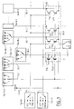
- FIG. 1 schematically presents a first example of implementation of the invention.
- K This figure represents part of an EEPROM memory erasable by groups of K memory cells, K whole number, and produced according to the invention. Typically, K will be equal to eight.
- this memory is organized matrically into N word lines WL and M bit lines BL, N and M being whole numbers.
- This memory comprises memory cells placed at the intersections of the word lines and the bit lines, each of the cells being in an electrical state representative of a binary logic state.
- the cells of the same group are connected to the same word line and to K separate bit lines.
- FIG. 1 there is shown a word line WL and a group CGR of memory cells connected to this word line.
- Each of the K cells (not all shown) is respectively connected to a bit line among K bit lines, bearing the references BL1 to BLK. It will of course be understood that a memory produced in accordance with the invention may contain a number of several tens or several hundred thousand storage cells.
- the K cells of the group of cells CGR each comprise a selection transistor, referenced respectively TS1 to TSK, and a floating gate storage transistor, referenced respectively TGF1 to TGFK.
- the selection and storage transistors are N-type transistors.
- the selection transistors TS1 to TSK have their drain connected respectively to bit lines BL1 to BLK. Their control grids are linked to the word line WL.
- each of the selection transistors TS1 to TSK has its source connected respectively to the drain of the transistors TGF1 to TGFK.
- the selection transistors make it possible to connect or isolate the drains of the transistors TGF1 to TGFK from the bit lines BL1 to BLK.
- control gates of the floating gate transistors of the group CGR are connected to each other and to a group selection circuit CS, the composition of which is described below.
- the selection circuit CS comprises a first and a second so-called group selection transistor, respectively referenced TSG1 and TSG2. These are two P-type transistors. Their drains are connected to each other and to the control gates of the TGF1 to TGFK transistors.
- the first group selection transistor TSG1 has its source connected to a so-called control line, referenced CL. Its control grid is connected to a first so-called selection line, referenced SL1.
- the second group selection transistor TSG2 has its source connected to a so-called reference line, referenced LREF. Its control grid is connected to a second so-called selection line, referenced SL2.
- the two group selection transistors TSG1 and TSG2 have their boxes connected to a common box line, referenced BUL. We will assume that all boxes of group selection transistors associated with the group of memory cells are connected to this line BUL, each group having an associated selection circuit comprising two group selection transistors.
- the lines CL, LREF, SL1 and SL2 are conductive lines allowing the control grids of the storage transistors TGF1 to TGFK to be brought to different potentials, depending on whether or not the cells comprising these transistors are selected, for reading, programming or erase their content.
- the content of the cells is determined through the electrical characteristics of the floating gate transistors. More precisely, the content of the cells will be qualified in relation to the presence or absence of electrons at the level of the floating grids.
- a positive reading voltage will be imposed on the drain of its floating gate transistor, the transistor cell selection being on, and the source of the floating gate transistor being connected to ground.
- its control gate being suitably positively biased, the current flowing through the channel of this transistor will be more or less important. By comparison of this current, which flows through the associated bit line, with a reference current, the electrical state of the cell and therefore its information content will be determined.
- the storage transistors In a third mode, called reading, the storage transistors will be polarized so as to make them passable, the value of the current flowing through their channel depending on the electrical state of their floating gate.
- the selection lines SL1 and SL2, of command CL, of reference LREF, of common source SREF, of common box BUL, of word WL and of bit BL will be brought to different potentials.
- GND and VCC potentials are available on memory connection pins.
- the other potentials will preferably be produced internally in the memory, which makes it possible to limit the number of connection pins of the memory.
- the potentials of absolute value greater than that of VCC will typically be produced from voltage boosting circuits, commonly called charge pumps, the realization of which is well known to those skilled in the art.
- the source switching circuit SW-S makes it possible to bring the potential of the common source line SREF to the ground potential GND or to put this line in a high impedance state.
- the N word line switching circuits SW-WL make it possible to carry the potential of the word lines WL to one of the potentials VCC, VP or GND.
- the M bit line switching circuits SW-BL make it possible to bring the potential of the bit lines BL to one of the potentials VCC, VS or GND, or to put these lines in a high impedance state.
- the first selection line switching circuits SW-SL1 make it possible to bring the potential of the first selection lines SL1 to one of the potentials VCC, VPP, HVH or GND.
- the second selection line switching circuits SW-SL2 make it possible to bring the potential of the second selection lines SL2 to one of the potentials VCC, VPP, or GND.
- the SW-BUL box switching circuit makes it possible to bring the potential of the common line of BUL box to one of the potentials VCC, VPP, or VREAD.
- the memory includes N control lines, so that all the groups of cells connected to the same word line WL have their first group selection transistors TSG1 connected to the same control line CL.
- the switching circuits SW-CL and SW-SL1 will be controlled in such a way that a single group of cells connected to the same word line WL is connected simultaneously to the command line CL associated with this word line.
- the number of control gates for floating-gate transistors connected simultaneously to a control line CL is limited to K. Therefore we will limit the equivalent induced capacity seen by this line CL. The rise time will therefore be limited to the potential of this line of the control grids connected to said line.
- the groups of cells whose cells are connected to K same bit lines have their first selection transistor TSG1 connected to the same first selection line SL1. Therefore, we will have a first selection line SL1 for K bit lines, which limits the size of the memory.
- the groups of cells whose cells are connected to K same bit lines will advantageously have their second group selection transistor TSG2 connected to the same second selection line SL2. There will thus be a second selection line SL2 for K bit lines.
- the groups of cells whose cells are connected to K same bit lines have their second group selection transistor TSG2 connected to the same reference line LREF.
- a reference line LREF is provided for K bit lines, which limits the size of the memory.
- the reference lines running parallel to the bit lines may be connected together, which will amount to having a single reference line. Indeed, these reference lines are constantly brought to the same VREAD potential.
- the LREF reference lines are used in such a way that the potentials of the control gates of the floating-gate transistors of the group cells are in a non-floating state when these control gates are isolated from the control lines CL. This avoids disturbance of the electrical states of the storage transistors, which could be modified by capacitive coupling. This would cause variations in the characteristics which could be more or less important depending on the cells, which is not desirable. Indeed, the behavior of cells in reading mode would be variable, which would induce variations in reaction time, or even uncertainties about the information content of cells.
- bit lines being grouped into sets of K lines these sets will be grouped two by two so that the groups of cells whose the cells are connected to one or the other of two sets of K grouped bit lines have their second group selection transistor TSG2 connected to the same reference line LREF.
- FIG. 4 shows two selection circuits CS 1 and CS 2 connected to the same control line CL.
- the circuits CS 1 and CS 2 are respectively connected to first selection lines SL1 1 and SL1 2 , to second selection lines SL2 1 and SL2 2 , and to a reference line LREF placed between the circuits CS 1 and CS 2 .
- FIG. 3 shows two selection circuits CS 1 and CS 2 connected respectively to control lines CL 1 and CL 2 , to word lines WL 1 and WL 2 , and to a common reference line LREF.
- the choice of positioning the reference lines parallel to the bit lines or the word lines will depend on the number of bit lines and word lines, on the surface and the possible shape of the memory.
- bit lines will be produced on a first metallization layer.
- the selection lines extending parallel to the bit lines, it will be the same for the latter if it is desired to limit the number of metallization layers.
- control lines will be made on a second metallization layer. Indeed, as they extend parallel to the word lines, it is necessary to make them on a different metallization layer to avoid short-circuiting the lines between them. Insofar as there are two metallization layers, it will be advantageous to make the word lines on the second metallization layer rather than a polysilicon layer. In fact, the resistivity is much lower for a metal line, which limits the heating and the stabilization time to a desired potential.
- first and second metallization layer we can physically realize these respectively above or below each other.
- VCC is imposed on the drain of the selection transistor, VP on the control gate of the selection transistor (in order to make it conducting), and HVN on the control gate of the storage transistor. (in order to inject electrons from its floating gate to its drain).
- GND (or a high impedance state) is imposed on the drain of the selection transistor, VP on the control gate of the selection transistor, and VREAD on the control gate of the storage transistor, so that there is no injection of electrons from the floating gate to the drain.
- GND (or a high impedance state) is imposed on the drain of the selection transistor, GND on the control gate of the selection transistor, and VREAD on the control gate of the storage transistor.
- GND is imposed on the drain of the selection transistor, VCC on the control gate of the selection transistor (in order to turn it on), and VPP on the control gate of the storage transistor , in order to produce an attractive field.
- GND is imposed on the drain of the selection transistor, VCC on the control gate of the selection transistor, and VREAD on the control gate of the storage transistor, so that the floating gate - drain potential difference is insufficient to erase the content of the storage transistor.
- GND is imposed on the drain of the selection transistor, GND on the control gate of the selection transistor, and VREAD on the control gate of the storage transistor.
- GND is imposed on the drain of the selection transistor, GND on the control gate of the selection transistor, and VREAD on the control gate of the transistor memorization.
- the word lines corresponding to the GND potential are taken.
- VS is imposed on the drain of the selection transistor, VCC on the control gate of the selection transistor (so that it is on), and VREAD on the control gate of the storage transistor , so that it is also passing.
- a state of high impedance is imposed on the drain of the selection transistor, VCC on the control gate of the selection transistor, and VREAD on the control gate of the storage transistor.
- VS is imposed on the drain of the selection transistor, GND on the control gate of the selection transistor (so that it is blocked), and VREAD on the control gate of the storage transistor.
- a high impedance state is imposed on the drain of the selection transistor, GND on the control gate of the selection transistor, and VREAD on the gate for controlling the storage transistor.
- control circuits of the switching circuits will not be detailed. Typically, these circuits will be combinational logic circuits producing control signals according to the mode chosen, the word line selected and the bit line (s) selected.
Applications Claiming Priority (2)
| Application Number | Priority Date | Filing Date | Title |
|---|---|---|---|
| FR9507622A FR2735896B1 (fr) | 1995-06-21 | 1995-06-21 | Memoire eeprom programmable et effacable par effet de fowler-nordheim |
| FR9507622 | 1995-06-21 |
Publications (2)
| Publication Number | Publication Date |
|---|---|
| EP0750313A1 true EP0750313A1 (de) | 1996-12-27 |
| EP0750313B1 EP0750313B1 (de) | 1998-09-30 |
Family
ID=9480373
Family Applications (1)
| Application Number | Title | Priority Date | Filing Date |
|---|---|---|---|
| EP96470012A Expired - Lifetime EP0750313B1 (de) | 1995-06-21 | 1996-06-17 | EEPROM-Speicher, der mit Fowler-Nordheim Effekt programmiert und gelöscht wird |
Country Status (5)
| Country | Link |
|---|---|
| US (1) | US6011717A (de) |
| EP (1) | EP0750313B1 (de) |
| JP (1) | JPH097379A (de) |
| DE (1) | DE69600711T2 (de) |
| FR (1) | FR2735896B1 (de) |
Cited By (3)
| Publication number | Priority date | Publication date | Assignee | Title |
|---|---|---|---|---|
| GB2321735A (en) * | 1997-01-30 | 1998-08-05 | Motorola Inc | Circuit and method for sharing a latch between a bit line and an erase line in a non-volatile memory |
| WO1999004399A1 (de) * | 1997-07-14 | 1999-01-28 | Infineon Technologies Ag | Halbleiterspeicher mit nicht-flüchtigen zwei-transistor-speicherzellen |
| FR2776820A1 (fr) * | 1998-03-24 | 1999-10-01 | Sgs Thomson Microelectronics | Memoire a grille flottante electriquement effacable organisee en mots |
Families Citing this family (7)
| Publication number | Priority date | Publication date | Assignee | Title |
|---|---|---|---|---|
| DE69832609D1 (de) * | 1998-09-30 | 2006-01-05 | St Microelectronics Srl | Emulierte EEPROM Speicheranordnung und entsprechendes Verfahren |
| US6215701B1 (en) * | 1998-12-22 | 2001-04-10 | Oki Semiconductor | Nonvolatile memory cell structure for integration with semiconductor logic devices and method of using same |
| US6650563B2 (en) * | 2002-04-23 | 2003-11-18 | Broadcom Corporation | Compact and highly efficient DRAM cell |
| EP1814121A1 (de) * | 2006-01-31 | 2007-08-01 | STMicroelectronics S.r.l. | Nichtflüchtige EEPROM Speicheranordnung |
| US8320191B2 (en) | 2007-08-30 | 2012-11-27 | Infineon Technologies Ag | Memory cell arrangement, method for controlling a memory cell, memory array and electronic device |
| EP2302635B1 (de) * | 2009-09-18 | 2016-01-13 | STMicroelectronics Srl | Verfahren zum Vormagnetisieren einer nichtflüchtigen EEPROM-Speicheranordnung und entsprechende nichtflüchtige EEPROM-Speicheranordnung |
| US8995161B2 (en) | 2011-06-10 | 2015-03-31 | Micron Technology, Inc. | Apparatus and methods to perform read-while write (RWW) operations |
Citations (2)
| Publication number | Priority date | Publication date | Assignee | Title |
|---|---|---|---|---|
| EP0332274A2 (de) * | 1988-03-09 | 1989-09-13 | Koninklijke Philips Electronics N.V. | EEPROM mit durch Daten gesteuerten Löschungs- und Schreibmodus |
| EP0637035A1 (de) * | 1993-07-29 | 1995-02-01 | STMicroelectronics S.r.l. | Schaltungsstruktur für Speichermatrix und entsprechende Herstellungsverfahren |
Family Cites Families (6)
| Publication number | Priority date | Publication date | Assignee | Title |
|---|---|---|---|---|
| US5077691A (en) * | 1989-10-23 | 1991-12-31 | Advanced Micro Devices, Inc. | Flash EEPROM array with negative gate voltage erase operation |
| JP2835215B2 (ja) * | 1991-07-25 | 1998-12-14 | 株式会社東芝 | 不揮発性半導体記憶装置 |
| US5477499A (en) * | 1993-10-13 | 1995-12-19 | Advanced Micro Devices, Inc. | Memory architecture for a three volt flash EEPROM |
| DE69523743T2 (de) * | 1994-03-03 | 2002-08-01 | Rohm Corp | Überlöschungsdetektion in einer niederspannungs-eintransistor-flash-eeprom-zelle unter verwendung von fowler-nordheim-programmierung und -löschung |
| GB9417266D0 (en) * | 1994-08-26 | 1994-10-19 | Inmos Ltd | Testing a non-volatile memory |
| GB9423032D0 (en) * | 1994-11-15 | 1995-01-04 | Sgs Thomson Microelectronics | Bit line sensing in a memory array |
-
1995
- 1995-06-21 FR FR9507622A patent/FR2735896B1/fr not_active Expired - Fee Related
-
1996
- 1996-06-14 JP JP17594296A patent/JPH097379A/ja not_active Withdrawn
- 1996-06-17 EP EP96470012A patent/EP0750313B1/de not_active Expired - Lifetime
- 1996-06-17 DE DE69600711T patent/DE69600711T2/de not_active Expired - Fee Related
- 1996-06-19 US US08/666,849 patent/US6011717A/en not_active Expired - Fee Related
Patent Citations (2)
| Publication number | Priority date | Publication date | Assignee | Title |
|---|---|---|---|---|
| EP0332274A2 (de) * | 1988-03-09 | 1989-09-13 | Koninklijke Philips Electronics N.V. | EEPROM mit durch Daten gesteuerten Löschungs- und Schreibmodus |
| EP0637035A1 (de) * | 1993-07-29 | 1995-02-01 | STMicroelectronics S.r.l. | Schaltungsstruktur für Speichermatrix und entsprechende Herstellungsverfahren |
Cited By (5)
| Publication number | Priority date | Publication date | Assignee | Title |
|---|---|---|---|---|
| GB2321735A (en) * | 1997-01-30 | 1998-08-05 | Motorola Inc | Circuit and method for sharing a latch between a bit line and an erase line in a non-volatile memory |
| WO1999004399A1 (de) * | 1997-07-14 | 1999-01-28 | Infineon Technologies Ag | Halbleiterspeicher mit nicht-flüchtigen zwei-transistor-speicherzellen |
| US6266274B1 (en) | 1997-07-14 | 2001-07-24 | Infineon Technologies Ag | Semiconductor memory with non-volatile two-transistor memory cells |
| FR2776820A1 (fr) * | 1998-03-24 | 1999-10-01 | Sgs Thomson Microelectronics | Memoire a grille flottante electriquement effacable organisee en mots |
| US6097631A (en) * | 1998-03-24 | 2000-08-01 | Stmicroelectronics S.A. | Electrically erasable floating-gate memory organized in words |
Also Published As
| Publication number | Publication date |
|---|---|
| US6011717A (en) | 2000-01-04 |
| EP0750313B1 (de) | 1998-09-30 |
| DE69600711D1 (de) | 1998-11-05 |
| FR2735896B1 (fr) | 1997-08-22 |
| JPH097379A (ja) | 1997-01-10 |
| DE69600711T2 (de) | 1999-03-04 |
| FR2735896A1 (fr) | 1996-12-27 |
Similar Documents
| Publication | Publication Date | Title |
|---|---|---|
| EP1342244B1 (de) | Seitenlöschbarer flash-speicher | |
| FR2825829A1 (fr) | Dispositif de memoire a semiconducteur ayant des reseaux de cellules de memoire permettant un acces selectif | |
| FR2480504A1 (fr) | Transistor programmable et effacable electriquement | |
| EP1727152B1 (de) | EEPROM-Speicherarchitektur | |
| FR2640797A1 (fr) | Dispositif de memoire electriquement effacable programmable a semi-conducteur et procede pour l'effacement et la programmation de celui-ci | |
| US7167392B1 (en) | Non-volatile memory cell with improved programming technique | |
| FR2652189A1 (fr) | Memoire eeprom "flash" a effacement par blocs. | |
| EP1495496A1 (de) | Elektrisch löschbare und programmiebare nichtflüchtige halbleiterspeicheranordnung mit einschichtigem gatematerial und entsprechende speicherfläche | |
| FR2987696A1 (fr) | Procede de lecture ecriture de cellules memoire non volatiles | |
| FR3029343A1 (fr) | Dispositif compact de memoire de type electriquement effacable et programmable | |
| FR3021804A1 (fr) | Cellule memoire non volatile duale comprenant un transistor d'effacement | |
| FR3025353A1 (fr) | Memoire non volatile composite a effacement par page ou par mot | |
| FR3021803A1 (fr) | Cellules memoire jumelles accessibles individuellement en lecture | |
| EP0750313B1 (de) | EEPROM-Speicher, der mit Fowler-Nordheim Effekt programmiert und gelöscht wird | |
| FR3025649A1 (fr) | Procede de polarisation d’un plan de source enterre d’une memoire non volatile a grilles de selection verticales | |
| FR3049380A1 (fr) | Amelioration des performances en lecture d'un dispositif de memoire non volatile, en particulier un dispositif de memoire non volatile avec transistor de selection enterre | |
| FR2826496A1 (fr) | Memoire eeprom protegee contre les effets d'un claquage de transistor d'acces | |
| FR2816750A1 (fr) | Memoire flash comprenant des moyens de controle de la tension de seuil de cellules memoire | |
| KR20040070218A (ko) | 2트랜지스터 플래시 메모리 셀과 그 어레이 판독 방법 및메모리 디바이스 | |
| WO2004021361A2 (fr) | Memoire eeprom comprenant un registre non volatile integre dans son plan memoire | |
| JP2004199837A (ja) | 不揮発性メモリ及びその書き込み方法 | |
| EP2337032A1 (de) | Verfahren zur Programmierung einer nichtflüchtigen elektrisch löschbaren und programmierbaren Speicherzelle und und dementsprechende Speicheranordnung | |
| FR2683664A1 (fr) | Memoire integree electriquement programmable a un seuil transistor. | |
| FR3006491A1 (fr) | Procede d’ecriture dans une memoire de type eeprom incluant un rafraichissement de cellules memoire | |
| FR2776820A1 (fr) | Memoire a grille flottante electriquement effacable organisee en mots |
Legal Events
| Date | Code | Title | Description |
|---|---|---|---|
| PUAI | Public reference made under article 153(3) epc to a published international application that has entered the european phase |
Free format text: ORIGINAL CODE: 0009012 |
|
| AK | Designated contracting states |
Kind code of ref document: A1 Designated state(s): DE FR GB IT |
|
| 17P | Request for examination filed |
Effective date: 19970318 |
|
| 17Q | First examination report despatched |
Effective date: 19970606 |
|
| GRAG | Despatch of communication of intention to grant |
Free format text: ORIGINAL CODE: EPIDOS AGRA |
|
| GRAG | Despatch of communication of intention to grant |
Free format text: ORIGINAL CODE: EPIDOS AGRA |
|
| GRAH | Despatch of communication of intention to grant a patent |
Free format text: ORIGINAL CODE: EPIDOS IGRA |
|
| GRAH | Despatch of communication of intention to grant a patent |
Free format text: ORIGINAL CODE: EPIDOS IGRA |
|
| GRAA | (expected) grant |
Free format text: ORIGINAL CODE: 0009210 |
|
| AK | Designated contracting states |
Kind code of ref document: B1 Designated state(s): DE FR GB IT |
|
| REF | Corresponds to: |
Ref document number: 69600711 Country of ref document: DE Date of ref document: 19981105 |
|
| GBT | Gb: translation of ep patent filed (gb section 77(6)(a)/1977) |
Effective date: 19981019 |
|
| RAP4 | Party data changed (patent owner data changed or rights of a patent transferred) |
Owner name: STMICROELECTRONICS S.A. |
|
| PLBE | No opposition filed within time limit |
Free format text: ORIGINAL CODE: 0009261 |
|
| STAA | Information on the status of an ep patent application or granted ep patent |
Free format text: STATUS: NO OPPOSITION FILED WITHIN TIME LIMIT |
|
| 26N | No opposition filed | ||
| REG | Reference to a national code |
Ref country code: GB Ref legal event code: IF02 |
|
| PGFP | Annual fee paid to national office [announced via postgrant information from national office to epo] |
Ref country code: GB Payment date: 20040616 Year of fee payment: 9 |
|
| PGFP | Annual fee paid to national office [announced via postgrant information from national office to epo] |
Ref country code: DE Payment date: 20040624 Year of fee payment: 9 |
|
| PGFP | Annual fee paid to national office [announced via postgrant information from national office to epo] |
Ref country code: FR Payment date: 20050608 Year of fee payment: 10 |
|
| PG25 | Lapsed in a contracting state [announced via postgrant information from national office to epo] |
Ref country code: IT Free format text: LAPSE BECAUSE OF NON-PAYMENT OF DUE FEES;WARNING: LAPSES OF ITALIAN PATENTS WITH EFFECTIVE DATE BEFORE 2007 MAY HAVE OCCURRED AT ANY TIME BEFORE 2007. THE CORRECT EFFECTIVE DATE MAY BE DIFFERENT FROM THE ONE RECORDED. Effective date: 20050617 Ref country code: GB Free format text: LAPSE BECAUSE OF NON-PAYMENT OF DUE FEES Effective date: 20050617 |
|
| PG25 | Lapsed in a contracting state [announced via postgrant information from national office to epo] |
Ref country code: DE Free format text: LAPSE BECAUSE OF NON-PAYMENT OF DUE FEES Effective date: 20060103 |
|
| GBPC | Gb: european patent ceased through non-payment of renewal fee |
Effective date: 20050617 |
|
| REG | Reference to a national code |
Ref country code: FR Ref legal event code: ST Effective date: 20070228 |
|
| PG25 | Lapsed in a contracting state [announced via postgrant information from national office to epo] |
Ref country code: FR Free format text: LAPSE BECAUSE OF NON-PAYMENT OF DUE FEES Effective date: 20060630 |