EP0750313A1 - EEPROM memory, programmed and erased by Fowler-Nordheim effect - Google Patents
EEPROM memory, programmed and erased by Fowler-Nordheim effect Download PDFInfo
- Publication number
- EP0750313A1 EP0750313A1 EP96470012A EP96470012A EP0750313A1 EP 0750313 A1 EP0750313 A1 EP 0750313A1 EP 96470012 A EP96470012 A EP 96470012A EP 96470012 A EP96470012 A EP 96470012A EP 0750313 A1 EP0750313 A1 EP 0750313A1
- Authority
- EP
- European Patent Office
- Prior art keywords
- lines
- cells
- selection
- group
- line
- Prior art date
- Legal status (The legal status is an assumption and is not a legal conclusion. Google has not performed a legal analysis and makes no representation as to the accuracy of the status listed.)
- Granted
Links
Images


Classifications
-
- G—PHYSICS
- G11—INFORMATION STORAGE
- G11C—STATIC STORES
- G11C16/00—Erasable programmable read-only memories
- G11C16/02—Erasable programmable read-only memories electrically programmable
- G11C16/04—Erasable programmable read-only memories electrically programmable using variable threshold transistors, e.g. FAMOS
- G11C16/0408—Erasable programmable read-only memories electrically programmable using variable threshold transistors, e.g. FAMOS comprising cells containing floating gate transistors
- G11C16/0433—Erasable programmable read-only memories electrically programmable using variable threshold transistors, e.g. FAMOS comprising cells containing floating gate transistors comprising cells containing a single floating gate transistor and one or more separate select transistors
-
- G—PHYSICS
- G11—INFORMATION STORAGE
- G11C—STATIC STORES
- G11C16/00—Erasable programmable read-only memories
- G11C16/02—Erasable programmable read-only memories electrically programmable
- G11C16/06—Auxiliary circuits, e.g. for writing into memory
- G11C16/10—Programming or data input circuits
- G11C16/14—Circuits for erasing electrically, e.g. erase voltage switching circuits
Definitions
- the invention relates to electrically programmable and erasable read-only memories, called EEPROMs. More particularly, it relates to a Fowler-Nordheim effect programmable EEPROM memory architecture.
- the memory cells of EEPROM memories are generally formed by a floating gate storage transistor and a selection transistor making it possible to connect the storage transistor to a word line and a bit line.
- EEPROM memories use the principle of non-volatile storage of charges on the floating gate of the floating gate transistor. Conventionally, the writing (we will speak in the following of the programming document) is done by injection by tunneling effect of electrons from the drain or the source towards the floating grid (or from the floating grid towards the drain or the source), and the erasure is done by injection by tunneling of electrons from the floating gate to the drain or the source (or from the drain or the source to the floating gate).
- EEPROM flash memories In these memories there is no selection transistor, and the storage transistors are directly connected to the word and bit lines. In this case, a global erasure of the storage cells is carried out. This type of memory makes it possible to reduce the size of the memory with equivalent storage capacity.
- the injection of electrons from the drain (or source) to the control gate of a storage transistor is conventionally done by grounding the drain (or source) of this transistor, applying a voltage relatively high positive on its control grid (of the order of + 15 volts) to create a attractive field, and application of a moderate positive voltage (+ 6 to + 9 volts) on the source (or the drain) to generate hot electrons.
- a voltage relatively high positive on its control grid of the order of + 15 volts
- the injection of electrons from the floating gate to the drain (or source) is done by applying a relatively high positive voltage (+ 15 volts) to the drain (or source), the control gate of the transistors storage being grounded, and the source (or drain) being floating.
- the negative charges are then extracted from the floating grid and directed towards the drain (or the source) by the Fowler-Nordheim effect.
- the thickness of the oxide between the floating gate and the drain (or the source) must be sufficiently small (of the order of 100 Angstroms or less) to allow injection by the Fowler-Nordheim effect.
- An object of the invention is to provide an EEPROM memory having an operation of the same type as that described above and a structure such that the erasure of the storage cells is operated selectively by groups of bits.
- the memory comprises second selection lines associated with the groups of cells and at least one reference line for conveying selection and reference potentials, and a second P-type group selection transistor per cell group to connect, via its channel, the floating gates of the storage transistors of the same group of cells to the reference line, the control gate of the second selection transistor being connected to one of the second selection lines, so that the potentials of the control grids of the storage transistors of the cells of the associated group are in a non-floating state when these control grids are isolated from the command line associated with the group.
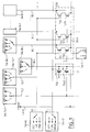
- FIG. 1 schematically presents a first example of implementation of the invention.
- K This figure represents part of an EEPROM memory erasable by groups of K memory cells, K whole number, and produced according to the invention. Typically, K will be equal to eight.
- this memory is organized matrically into N word lines WL and M bit lines BL, N and M being whole numbers.
- This memory comprises memory cells placed at the intersections of the word lines and the bit lines, each of the cells being in an electrical state representative of a binary logic state.
- the cells of the same group are connected to the same word line and to K separate bit lines.
- FIG. 1 there is shown a word line WL and a group CGR of memory cells connected to this word line.
- Each of the K cells (not all shown) is respectively connected to a bit line among K bit lines, bearing the references BL1 to BLK. It will of course be understood that a memory produced in accordance with the invention may contain a number of several tens or several hundred thousand storage cells.
- the K cells of the group of cells CGR each comprise a selection transistor, referenced respectively TS1 to TSK, and a floating gate storage transistor, referenced respectively TGF1 to TGFK.
- the selection and storage transistors are N-type transistors.
- the selection transistors TS1 to TSK have their drain connected respectively to bit lines BL1 to BLK. Their control grids are linked to the word line WL.
- each of the selection transistors TS1 to TSK has its source connected respectively to the drain of the transistors TGF1 to TGFK.
- the selection transistors make it possible to connect or isolate the drains of the transistors TGF1 to TGFK from the bit lines BL1 to BLK.
- control gates of the floating gate transistors of the group CGR are connected to each other and to a group selection circuit CS, the composition of which is described below.
- the selection circuit CS comprises a first and a second so-called group selection transistor, respectively referenced TSG1 and TSG2. These are two P-type transistors. Their drains are connected to each other and to the control gates of the TGF1 to TGFK transistors.
- the first group selection transistor TSG1 has its source connected to a so-called control line, referenced CL. Its control grid is connected to a first so-called selection line, referenced SL1.
- the second group selection transistor TSG2 has its source connected to a so-called reference line, referenced LREF. Its control grid is connected to a second so-called selection line, referenced SL2.
- the two group selection transistors TSG1 and TSG2 have their boxes connected to a common box line, referenced BUL. We will assume that all boxes of group selection transistors associated with the group of memory cells are connected to this line BUL, each group having an associated selection circuit comprising two group selection transistors.
- the lines CL, LREF, SL1 and SL2 are conductive lines allowing the control grids of the storage transistors TGF1 to TGFK to be brought to different potentials, depending on whether or not the cells comprising these transistors are selected, for reading, programming or erase their content.
- the content of the cells is determined through the electrical characteristics of the floating gate transistors. More precisely, the content of the cells will be qualified in relation to the presence or absence of electrons at the level of the floating grids.
- a positive reading voltage will be imposed on the drain of its floating gate transistor, the transistor cell selection being on, and the source of the floating gate transistor being connected to ground.
- its control gate being suitably positively biased, the current flowing through the channel of this transistor will be more or less important. By comparison of this current, which flows through the associated bit line, with a reference current, the electrical state of the cell and therefore its information content will be determined.
- the storage transistors In a third mode, called reading, the storage transistors will be polarized so as to make them passable, the value of the current flowing through their channel depending on the electrical state of their floating gate.
- the selection lines SL1 and SL2, of command CL, of reference LREF, of common source SREF, of common box BUL, of word WL and of bit BL will be brought to different potentials.
- GND and VCC potentials are available on memory connection pins.
- the other potentials will preferably be produced internally in the memory, which makes it possible to limit the number of connection pins of the memory.
- the potentials of absolute value greater than that of VCC will typically be produced from voltage boosting circuits, commonly called charge pumps, the realization of which is well known to those skilled in the art.
- the source switching circuit SW-S makes it possible to bring the potential of the common source line SREF to the ground potential GND or to put this line in a high impedance state.
- the N word line switching circuits SW-WL make it possible to carry the potential of the word lines WL to one of the potentials VCC, VP or GND.
- the M bit line switching circuits SW-BL make it possible to bring the potential of the bit lines BL to one of the potentials VCC, VS or GND, or to put these lines in a high impedance state.
- the first selection line switching circuits SW-SL1 make it possible to bring the potential of the first selection lines SL1 to one of the potentials VCC, VPP, HVH or GND.
- the second selection line switching circuits SW-SL2 make it possible to bring the potential of the second selection lines SL2 to one of the potentials VCC, VPP, or GND.
- the SW-BUL box switching circuit makes it possible to bring the potential of the common line of BUL box to one of the potentials VCC, VPP, or VREAD.
- the memory includes N control lines, so that all the groups of cells connected to the same word line WL have their first group selection transistors TSG1 connected to the same control line CL.
- the switching circuits SW-CL and SW-SL1 will be controlled in such a way that a single group of cells connected to the same word line WL is connected simultaneously to the command line CL associated with this word line.
- the number of control gates for floating-gate transistors connected simultaneously to a control line CL is limited to K. Therefore we will limit the equivalent induced capacity seen by this line CL. The rise time will therefore be limited to the potential of this line of the control grids connected to said line.
- the groups of cells whose cells are connected to K same bit lines have their first selection transistor TSG1 connected to the same first selection line SL1. Therefore, we will have a first selection line SL1 for K bit lines, which limits the size of the memory.
- the groups of cells whose cells are connected to K same bit lines will advantageously have their second group selection transistor TSG2 connected to the same second selection line SL2. There will thus be a second selection line SL2 for K bit lines.
- the groups of cells whose cells are connected to K same bit lines have their second group selection transistor TSG2 connected to the same reference line LREF.
- a reference line LREF is provided for K bit lines, which limits the size of the memory.
- the reference lines running parallel to the bit lines may be connected together, which will amount to having a single reference line. Indeed, these reference lines are constantly brought to the same VREAD potential.
- the LREF reference lines are used in such a way that the potentials of the control gates of the floating-gate transistors of the group cells are in a non-floating state when these control gates are isolated from the control lines CL. This avoids disturbance of the electrical states of the storage transistors, which could be modified by capacitive coupling. This would cause variations in the characteristics which could be more or less important depending on the cells, which is not desirable. Indeed, the behavior of cells in reading mode would be variable, which would induce variations in reaction time, or even uncertainties about the information content of cells.
- bit lines being grouped into sets of K lines these sets will be grouped two by two so that the groups of cells whose the cells are connected to one or the other of two sets of K grouped bit lines have their second group selection transistor TSG2 connected to the same reference line LREF.
- FIG. 4 shows two selection circuits CS 1 and CS 2 connected to the same control line CL.
- the circuits CS 1 and CS 2 are respectively connected to first selection lines SL1 1 and SL1 2 , to second selection lines SL2 1 and SL2 2 , and to a reference line LREF placed between the circuits CS 1 and CS 2 .
- FIG. 3 shows two selection circuits CS 1 and CS 2 connected respectively to control lines CL 1 and CL 2 , to word lines WL 1 and WL 2 , and to a common reference line LREF.
- the choice of positioning the reference lines parallel to the bit lines or the word lines will depend on the number of bit lines and word lines, on the surface and the possible shape of the memory.
- bit lines will be produced on a first metallization layer.
- the selection lines extending parallel to the bit lines, it will be the same for the latter if it is desired to limit the number of metallization layers.
- control lines will be made on a second metallization layer. Indeed, as they extend parallel to the word lines, it is necessary to make them on a different metallization layer to avoid short-circuiting the lines between them. Insofar as there are two metallization layers, it will be advantageous to make the word lines on the second metallization layer rather than a polysilicon layer. In fact, the resistivity is much lower for a metal line, which limits the heating and the stabilization time to a desired potential.
- first and second metallization layer we can physically realize these respectively above or below each other.
- VCC is imposed on the drain of the selection transistor, VP on the control gate of the selection transistor (in order to make it conducting), and HVN on the control gate of the storage transistor. (in order to inject electrons from its floating gate to its drain).
- GND (or a high impedance state) is imposed on the drain of the selection transistor, VP on the control gate of the selection transistor, and VREAD on the control gate of the storage transistor, so that there is no injection of electrons from the floating gate to the drain.
- GND (or a high impedance state) is imposed on the drain of the selection transistor, GND on the control gate of the selection transistor, and VREAD on the control gate of the storage transistor.
- GND is imposed on the drain of the selection transistor, VCC on the control gate of the selection transistor (in order to turn it on), and VPP on the control gate of the storage transistor , in order to produce an attractive field.
- GND is imposed on the drain of the selection transistor, VCC on the control gate of the selection transistor, and VREAD on the control gate of the storage transistor, so that the floating gate - drain potential difference is insufficient to erase the content of the storage transistor.
- GND is imposed on the drain of the selection transistor, GND on the control gate of the selection transistor, and VREAD on the control gate of the storage transistor.
- GND is imposed on the drain of the selection transistor, GND on the control gate of the selection transistor, and VREAD on the control gate of the transistor memorization.
- the word lines corresponding to the GND potential are taken.
- VS is imposed on the drain of the selection transistor, VCC on the control gate of the selection transistor (so that it is on), and VREAD on the control gate of the storage transistor , so that it is also passing.
- a state of high impedance is imposed on the drain of the selection transistor, VCC on the control gate of the selection transistor, and VREAD on the control gate of the storage transistor.
- VS is imposed on the drain of the selection transistor, GND on the control gate of the selection transistor (so that it is blocked), and VREAD on the control gate of the storage transistor.
- a high impedance state is imposed on the drain of the selection transistor, GND on the control gate of the selection transistor, and VREAD on the gate for controlling the storage transistor.
- control circuits of the switching circuits will not be detailed. Typically, these circuits will be combinational logic circuits producing control signals according to the mode chosen, the word line selected and the bit line (s) selected.
Abstract
Description
L'invention concerne les mémoires mortes électriquement programmables et effaçables, dites EEPROM. Plus particulièrement, elle concerne une architecture de mémoire EEPROM programmable et effaçable par effet de Fowler-Nordheim.The invention relates to electrically programmable and erasable read-only memories, called EEPROMs. More particularly, it relates to a Fowler-Nordheim effect programmable EEPROM memory architecture.
Les cellules de mémorisation des mémoires EEPROM sont généralement formées d'un transistor de mémorisation à grille flottante et d'un transistor de sélection permettant de relier le transistor de mémorisation à une ligne de mot et une ligne de bit. Les mémoires EEPROM utilisent le principe du stockage non volatil de charges sur la grille flottante du transistor à grille flottante. Classiquement, l'écriture (on parlera dans la suite du document de programmation) se fait par injection par effet tunnel d'électrons du drain ou de la source vers la grille flottante (ou de la grille flottante vers le drain ou la source), et l'effacement se fait par injection par effet tunnel d'électrons de la grille flottante vers le drain ou la source (ou du drain ou de la source vers la grille flottante). On connaît également des mémoires EEPROM dites flash. Dans ces mémoires il n'y a pas de transistor de sélection, et les transistors de mémorisation sont directement reliés aux lignes de mot et de bit. On procède dans ce cas à un effacement global des cellules de mémorisation. Ce type de mémoire permet de diminuer la taille de la mémoire à capacité de mémorisation équivalente.The memory cells of EEPROM memories are generally formed by a floating gate storage transistor and a selection transistor making it possible to connect the storage transistor to a word line and a bit line. EEPROM memories use the principle of non-volatile storage of charges on the floating gate of the floating gate transistor. Conventionally, the writing (we will speak in the following of the programming document) is done by injection by tunneling effect of electrons from the drain or the source towards the floating grid (or from the floating grid towards the drain or the source), and the erasure is done by injection by tunneling of electrons from the floating gate to the drain or the source (or from the drain or the source to the floating gate). Also known as EEPROM flash memories. In these memories there is no selection transistor, and the storage transistors are directly connected to the word and bit lines. In this case, a global erasure of the storage cells is carried out. This type of memory makes it possible to reduce the size of the memory with equivalent storage capacity.
L'injection d'électrons du drain (ou de la source) vers la grille de commande d'un transistor de mémorisation se fait classiquement par mise à la masse du drain (ou de la source) de ce transistor, application d'une tension positive relativement élevée sur sa grille de commande (de l'ordre de + 15 volts) pour créer un champ attractif, et application d'une tension positive modérée (+ 6 à + 9 volts) sur la source (ou le drain) pour générer des électrons chauds. Quand un nombre suffisamment important de charges négatives s'est accumulé sur la grille flottante le potentiel de la grille flottante atteint le potentiel de seuil du transistor et empêche le passage de courant dans un mode de lecture.The injection of electrons from the drain (or source) to the control gate of a storage transistor is conventionally done by grounding the drain (or source) of this transistor, applying a voltage relatively high positive on its control grid (of the order of + 15 volts) to create a attractive field, and application of a moderate positive voltage (+ 6 to + 9 volts) on the source (or the drain) to generate hot electrons. When a sufficiently large number of negative charges has accumulated on the floating gate the potential of the floating gate reaches the threshold potential of the transistor and prevents the passage of current in a reading mode.
L'injection d'électrons de la grille flottante vers le drain (ou la source) se fait par application d'une tension positive relativement élevée (+ 15 volts) sur le drain (ou la source), la grille de commande des transistors de mémorisation étant mise à la masse, et la source (ou le drain) étant flottant. Les charges négatives sont alors extraites de la grille flottante et dirigées vers le drain (ou la source) par effet Fowler-Nordheim. L'épaisseur de l'oxyde entre la grille flottante et le drain (ou la source) doit être suffisamment faible (de l'ordre de 100 Angströms ou moins) pour permettre l'injection par effet Fowler-Nordheim.The injection of electrons from the floating gate to the drain (or source) is done by applying a relatively high positive voltage (+ 15 volts) to the drain (or source), the control gate of the transistors storage being grounded, and the source (or drain) being floating. The negative charges are then extracted from the floating grid and directed towards the drain (or the source) by the Fowler-Nordheim effect. The thickness of the oxide between the floating gate and the drain (or the source) must be sufficiently small (of the order of 100 Angstroms or less) to allow injection by the Fowler-Nordheim effect.
Ce type de mémoire présente des inconvénients, notamment dans la mise en oeuvre de l'éjection des électrons des grilles flottantes :
- le courant drain-substrat (ou source-substrat) pendant l'éjection est relativement important et impose en pratique, pour des mémoires de grandes capacités, de disposer d'une source de tension positive élevée qui soit externe au circuit,
- une tension inverse relativement importante est générée entre le drains (ou les sources) et le substrat pendant l'éjection. En pratique cela impose d'utiliser des drains (ou sources) à double diffusion, ce qui diminue la densité d'implantation des cellules,
- l'application d'une tension positive relativement élevée durant l'effacement sur les drains (ou les sources) augmente la probabilité de création de trous chauds, par effet d'avalanche à la surface de la jonction drain-substrat (ou source-substrat), ceux-ci étant piégés dans l'oxyde mince situé sous la grille flottante.
- the drain-substrate current (or source-substrate) during ejection is relatively large and in practice requires, for large-capacity memories, to have a source of high positive voltage which is external to the circuit,
- a relatively large reverse voltage is generated between the drains (or sources) and the substrate during ejection. In practice this requires the use of double diffusion drains (or sources), which reduces the density of implantation of the cells,
- the application of a relatively high positive voltage during the erasure on the drains (or the sources) increases the probability of hot holes being created, by an avalanche effect on the surface of the drain-substrate (or source-substrate) junction, these being trapped in the thin oxide located under the floating grid.
Pour plus de précisions sur ces phénomènes, on se reportera au brevet US-5 077 691 de Advanced Micro Devices Inc.For more details on these phenomena, see US Pat. No. 5,077,691 to Advanced Micro Devices Inc.
Dans ce document il est proposé d'effacer les cellules par application d'une tension négative relativement élevée (- 12 à - 17 volts, sur les grilles de commande, une tension positive relativement faible (+ 0.5 à + 5 volts) étant imposée sur les sources, le substrat étant relié à la masse, et les drains étant laissés en haute impédance. Ainsi, on peut induire un effet Fowler-Nordheim tout en gardant une tension inverse source-substrat inférieur à + 5 volts. Le courant de fuite de la source vers le substrat est réduit, permettant d'alimenter la mémoire avec une seule source de tension positive externe (+ 5 volts). D'autre part cela permet d'utiliser des sources comprenant une seule diffusion, ce qui limite la surface des cellules. Enfin, on peut éliminer la création de trous chauds, ce qui augmente la fiabilité de la mémoire.In this document, it is proposed to erase the cells by applying a relatively high negative voltage (- 12 to - 17 volts, on the control grids, a relatively low positive voltage (+ 0.5 to + 5 volts) being imposed on the sources, the substrate being connected to ground, and the drains being left in high impedance. Thus, one can induce a Fowler-Nordheim effect while keeping a reverse source-substrate voltage of less than + 5 volts. the source towards the substrate is reduced, making it possible to supply the memory with a single source of external positive voltage (+ 5 volts). On the other hand it allows the use of sources comprising a single diffusion, which limits the surface of the Finally, we can eliminate the creation of hot holes, which increases the reliability of the memory.
Un but de l'invention est de proposer une mémoire EEPROM ayant un fonctionnement de même type que celui décrit ci-dessus et une structure telle que l'effacement des cellules de mémorisation soit opérée sélectivement par groupes de bits.An object of the invention is to provide an EEPROM memory having an operation of the same type as that described above and a structure such that the erasure of the storage cells is operated selectively by groups of bits.
Ainsi, l'invention propose une mémoire EEPROM organisée matriciellement en N lignes de mot et M lignes de bit, N et M étant des nombres entiers, comprenant
- des cellules de mémorisation placées aux intersections des lignes de mots et des lignes de bits, ces cellules de mémorisation comprenant des transistors de mémorisation à grille flottante de type N pour mémoriser des états électriques, les cellules de mémorisation étant regroupées en groupes de K cellules, K nombre entier, les cellules d'un même groupe étant reliées à une même ligne de mot et à K lignes de bit distinctes,
- des premières lignes de sélection et des lignes de commande, associées aux groupes de cellules, pour véhiculer des potentiels de sélection et de commande,
- un premier transistor de sélection de groupe de type P par groupe de cellule pour relier, via son canal, les grilles flottantes des transistors de mémorisation d'un même groupe de cellules à une des lignes de commande, la grille de commande du premier transistor de sélection étant reliée à une des premières ligne de sélection, quand on souhaite programmer, effacer, ou lire le contenu des cellules du groupe de cellules auquel est associé le premier transistor de sélection de groupe.
- storage cells placed at the intersections of word lines and bit lines, these storage cells comprising N-type floating gate storage transistors for storing electrical states, the storage cells memorization being grouped into groups of K cells, K whole number, the cells of the same group being connected to the same word line and to K distinct bit lines,
- first selection lines and command lines, associated with groups of cells, to convey selection and command potentials,
- a first P-type group selection transistor per cell group for connecting, via its channel, the floating gates of the storage transistors of the same group of cells to one of the control lines, the control gate of the first transistor selection being linked to one of the first selection lines, when it is desired to program, erase or read the content of the cells of the group of cells with which the first group selection transistor is associated.
Dans une version préférée, la mémoire comprend des deuxièmes lignes de sélection associées au groupes de cellules et au moins une ligne de référence pour véhiculer des potentiels de sélection et de référence, et un deuxième transistor de sélection de groupe de type P par groupe de cellule pour relier, via son canal, les grilles flottantes des transistors de mémorisation d'un même groupe de cellules à la ligne de référence, la grille de commande du deuxième transistor de sélection étant reliée à une des deuxièmes ligne de sélection, de telle manière que les potentiels des grilles de commande des transistors de mémorisation des cellules du groupe associé soient dans un état non flottant quand ces grilles de commande sont isolées de la ligne de commande associée au groupe.In a preferred version, the memory comprises second selection lines associated with the groups of cells and at least one reference line for conveying selection and reference potentials, and a second P-type group selection transistor per cell group to connect, via its channel, the floating gates of the storage transistors of the same group of cells to the reference line, the control gate of the second selection transistor being connected to one of the second selection lines, so that the potentials of the control grids of the storage transistors of the cells of the associated group are in a non-floating state when these control grids are isolated from the command line associated with the group.
D'autres particularités et avantages apparaîtront à la lecture de la description ci-après d'exemples de mise en oeuvre de l'invention, à lire conjointement aux dessins annexés dans lesquels :
- la figure 1 représente schématiquement un premier exemple de mise en oeuvre de l'invention,
- la figure 2 représente schématiquement un deuxième exemple de mise en oeuvre de l'invention
- la figure 3 représente schématiquement un troisième exemple de mise en oeuvre de l'invention
- la figure 4 représente schématiquement un quatrième exemple de mise en oeuvre de l'invention
- Figure 1 schematically shows a first example of implementation of the invention,
- FIG. 2 schematically represents a second example of implementation of the invention
- FIG. 3 schematically represents a third example of implementation of the invention
- FIG. 4 schematically represents a fourth example of implementation of the invention
La figure 1 présente schématiquement un premier exemple de mise en oeuvre de l'invention.FIG. 1 schematically presents a first example of implementation of the invention.
Cette figure représente une partie d'une mémoire EEPROM effaçable par groupes de K cellules de mémorisation, K nombre entier, et réalisée selon l'invention. Typiquement, K sera égal à huit.This figure represents part of an EEPROM memory erasable by groups of K memory cells, K whole number, and produced according to the invention. Typically, K will be equal to eight.
On suppose que cette mémoire est organisée matriciellement en N lignes de mot WL et M lignes de bit BL, N et M étant des nombres entiers.It is assumed that this memory is organized matrically into N word lines WL and M bit lines BL, N and M being whole numbers.
Cette mémoire comprend des cellules de mémorisation placées aux intersections des lignes de mots et des lignes de bits, chacune des cellules étant dans un état électrique représentatif d'un état logique binaire. Les cellules d'un même groupe sont reliées à une même ligne de mot et à K lignes de bit distinctes.This memory comprises memory cells placed at the intersections of the word lines and the bit lines, each of the cells being in an electrical state representative of a binary logic state. The cells of the same group are connected to the same word line and to K separate bit lines.
Sur la figure 1, on a représenté une ligne de mot WL et un groupe CGR de cellules de mémorisation reliées à cette ligne de mot. Chacune des K cellules (non toutes représentées) est respectivement reliée à une ligne de bit parmi K lignes de bit, portant les références BL1 à BLK. On comprendra bien sûr qu'une mémoire réalisée conformément à l'invention pourra contenir un nombre de plusieurs dizaines ou plusieurs centaines de milliers de cellules de mémorisation.In Figure 1, there is shown a word line WL and a group CGR of memory cells connected to this word line. Each of the K cells (not all shown) is respectively connected to a bit line among K bit lines, bearing the references BL1 to BLK. It will of course be understood that a memory produced in accordance with the invention may contain a number of several tens or several hundred thousand storage cells.
Les K cellules du groupe de cellules CGR comprennent chacune un transistor de sélection, référencés respectivement TS1 à TSK, et un transistor de mémorisation à grille flottante, référencés respectivement TGF1 à TGFK. Dans l'exemple décrit, on supposera que la mémoire est réalisée de manière classique, en technologie MOS, à partir d'un substrat de type P. Les transistors de sélection et de mémorisation sont des transistors de type N. Les transistors de sélection TS1 à TSK ont leur drain relié respectivement aux lignes de bit BL1 à BLK. Leur grilles de commande sont reliées à la ligne de mot WL. Enfin, chacun des transistors de sélection TS1 à TSK a sa source reliée respectivement au drain des transistors TGF1 à TGFK. Les transistors de sélection permettent de relier ou d'isoler les drains des transistors TGF1 à TGFK des lignes de bit BL1 à BLK.The K cells of the group of cells CGR each comprise a selection transistor, referenced respectively TS1 to TSK, and a floating gate storage transistor, referenced respectively TGF1 to TGFK. In the example described, we assume that the memory is produced conventionally, in MOS technology, from a P-type substrate. The selection and storage transistors are N-type transistors. The selection transistors TS1 to TSK have their drain connected respectively to bit lines BL1 to BLK. Their control grids are linked to the word line WL. Finally, each of the selection transistors TS1 to TSK has its source connected respectively to the drain of the transistors TGF1 to TGFK. The selection transistors make it possible to connect or isolate the drains of the transistors TGF1 to TGFK from the bit lines BL1 to BLK.
Les grilles de commande des transistors à grille flottante du groupe CGR sont reliées entre elles et à un circuit de sélection de groupe CS dont la composition est décrite ci-après.The control gates of the floating gate transistors of the group CGR are connected to each other and to a group selection circuit CS, the composition of which is described below.
On supposera que les sources des transistors à grille flottante TGF1 à TGFK des cellules de mémorisation de la mémoire sont toutes reliées à une ligne de source commune SREF.It will be assumed that the sources of the floating gate transistors TGF1 to TGFK of the memory storage cells are all connected to a common source line SREF.
Le circuit de sélection CS comprend un premier et un deuxième transistor dits de sélection de groupe, référencés respectivement TSG1 et TSG2. Ce sont deux transistors de type P. Leurs drains sont reliés entre eux et aux grilles de commande des transistors TGF1 à TGFK.The selection circuit CS comprises a first and a second so-called group selection transistor, respectively referenced TSG1 and TSG2. These are two P-type transistors. Their drains are connected to each other and to the control gates of the TGF1 to TGFK transistors.
Le premier transistor de sélection de groupe TSG1 a sa source reliée à une ligne dite de commande, référencée CL. Sa grille de commande est reliée à une première ligne dite de sélection, référencée SL1.The first group selection transistor TSG1 has its source connected to a so-called control line, referenced CL. Its control grid is connected to a first so-called selection line, referenced SL1.
Le deuxième transistor de sélection de groupe TSG2 a sa source reliée à une ligne dite de référence, référencée LREF. Sa grille de commande est reliée à une deuxième ligne dite de sélection, référencée SL2.The second group selection transistor TSG2 has its source connected to a so-called reference line, referenced LREF. Its control grid is connected to a second so-called selection line, referenced SL2.
Les deux transistors de sélection de groupe TSG1 et TSG2 ont leurs caissons reliés à une ligne de caisson commune, référencée BUL. On supposera que tous les caissons des transistors de sélection de groupe associés aux groupe de cellules de la mémoire sont reliés à cette ligne BUL, chaque groupe ayant un circuit de sélection associé comprenant deux transistors de sélection de groupe.The two group selection transistors TSG1 and TSG2 have their boxes connected to a common box line, referenced BUL. We will assume that all boxes of group selection transistors associated with the group of memory cells are connected to this line BUL, each group having an associated selection circuit comprising two group selection transistors.
Les lignes CL, LREF, SL1 et SL2 sont des lignes conductrices permettant de porter les grilles de commande des transistors de mémorisatiOn TGF1 à TGFK à différents potentiels, selon que l'on sélectionne ou non les cellules comprenant ces transistors, pour lire, programmer ou effacer leur contenu.The lines CL, LREF, SL1 and SL2 are conductive lines allowing the control grids of the storage transistors TGF1 to TGFK to be brought to different potentials, depending on whether or not the cells comprising these transistors are selected, for reading, programming or erase their content.
La mémoire comprend :
- un circuit SW-S de commutation de source relié à la ligne de source commune SREF, permettant de commander le potentiel de cette ligne de source,
- N circuits SW-WL de commutation de ligne de mot, reliés chacun à une des N lignes de mot WL, pour commander les potentiels des lignes de mot,
- M circuits SW-BL de commutation de ligne de bit, reliés chacun à une des M lignes de bit BL, pour commander les potentiels des lignes de bit,
- des premiers et deuxièmes circuits SW-SL1 et SW-SL2 de commutation de ligne de sélection, reliés respectivement aux premières et deuxièmes lignes de sélection, pour commander les potentiels de ces lignes,
- un circuit SW-BUL de commutation de caisson, relié à la ligne de caisson commune BUL pour commander le potentiel de cette ligne.
- a source switching circuit SW-S connected to the common source line SREF, making it possible to control the potential of this source line,
- N word line switching circuits SW-WL, each connected to one of the N word lines WL, for controlling the potentials of the word lines,
- M bit line switching circuits SW-BL, each connected to one of the M bit lines BL, for controlling the potentials of the bit lines,
- first and second selection line switching circuits SW-SL1 and SW-SL2, connected respectively to the first and second selection lines, for controlling the potentials of these lines,
- a SW-BUL box switching circuit, connected to the common box line BUL to control the potential of this line.
Comme on l'a dit, le contenu des cellules se détermine au travers des caractéristiques électriques des transistors à grille flottante. Plus précisément, on qualifiera le contenu des cellules par rapport à la présence ou l'absence d'électrons au niveau des grilles flottantes. Dans un mode de lecture d'une cellule, on imposera une tension positive de lecture sur le drain de son transistor à grille flottante, le transistor de sélection de la cellule étant passant, et la source du transistor à grille flottante étant reliée à la masse. Selon la présence d'électrons ou non sur la grille flottante du transistor de mémorisation, sa grille de commande étant polarisée positivement de manière adéquate, le courant parcourant le canal de ce transistor sera plus ou moins important. Par comparaison de ce courant, qui parcourt la ligne de bit associée, avec un courant de référence on determinera l'état électrique de la cellule et donc son contenu informationnel.As has been said, the content of the cells is determined through the electrical characteristics of the floating gate transistors. More precisely, the content of the cells will be qualified in relation to the presence or absence of electrons at the level of the floating grids. In a cell reading mode, a positive reading voltage will be imposed on the drain of its floating gate transistor, the transistor cell selection being on, and the source of the floating gate transistor being connected to ground. Depending on the presence of electrons or not on the floating gate of the storage transistor, its control gate being suitably positively biased, the current flowing through the channel of this transistor will be more or less important. By comparison of this current, which flows through the associated bit line, with a reference current, the electrical state of the cell and therefore its information content will be determined.
Dans l'exemple décrit on considérera par exemple que la présence d'électrons représente un état effacé et que l'absence d'électrons représente un état programmé. On pourrait tout aussi bien convenir de la convention inverse. On ne décrira pas ici les dispositifs (amplificateurs de lecture, décodeurs de lignes de mot et de ligne de bit, etc) qui constituent classiquement une mémoire, l'invention se rapportant spécifiquement à l'architecture du plan mémoire.In the example described, it will be considered for example that the presence of electrons represents an erased state and that the absence of electrons represents a programmed state. We could just as easily agree to the opposite convention. The devices (reading amplifiers, word line and bit line decoders, etc.) which conventionally constitute a memory will not be described here, the invention specifically referring to the architecture of the memory plane.
On distinguera trois types d'opération sur les cellules.We will distinguish three types of operation on cells.
Dans un premier mode, dit de programmation, on injectera des électrons des grilles flottantes des transistors de mémorisation vers leurs drains.In a first mode, called programming, we will inject electrons from the floating gates of the storage transistors to their drains.
Dans un deuxième mode, dit d'effacement, on injectera des électrons des drains des transistors de mémorisation vers leurs grilles flottantes.In a second mode, called erasure, electrons will be injected from the drains of the storage transistors to their floating gates.
Dans un troisième mode, dit de lecture, on polarisera les transistors de mémorisation de manière à les rendre passants, la valeur du courant parcourant leur canal dépendant de l'état électrique de leur grille flottante.In a third mode, called reading, the storage transistors will be polarized so as to make them passable, the value of the current flowing through their channel depending on the electrical state of their floating gate.
Dans ces différents modes les lignes de sélection SL1 et SL2, de commande CL, de référence LREF, de source commune SREF, de caisson commun BUL, de mot WL et de bit BL seront portées à différents potentiels.In these different modes, the selection lines SL1 and SL2, of command CL, of reference LREF, of common source SREF, of common box BUL, of word WL and of bit BL will be brought to different potentials.
Dans l'exemple illustré on utilise les potentiels suivants :
- un potentiel de masse GND = o v et un potentiel d'alimentation VCC = + 5 V (fournis par l'extérieur),
- un potentiel d'effacement VPP = + 15 V,
- un potentiel de programmation HVN = - 8 V,
- un potentiel de commande de programmation HVH = - 10V,
- un potentiel de sélection de ligne de mot en programmation VP = + 7 V,
- un potentiel de sélection de ligne de bit en lecture VS = + 2 V,
- un potentiel de commande de lecture VREAD = + 2.3 V.
- a ground potential GND = ov and a supply potential VCC = + 5 V (supplied from the outside),
- a potential for erasure VPP = + 15 V,
- HVN programming potential = - 8 V,
- a programming control potential HVH = - 10V,
- word line selection potential in programming VP = + 7 V,
- a bit line selection potential in reading VS = + 2 V,
- a read command potential VREAD = + 2.3 V.
On notera HiZ un état de haute impédance.We will note HiZ a state of high impedance.
Typiquement les potentiels GND et VCC sont disponibles sur des broches de connexion de la mémoire. Les autres potentiels seront de préférence produits de manière interne à la mémoire, ce qui permet de limiter le nombre de broches de connexion de la mémoire. Les potentiels de valeur absolue plus grande que celle de VCC seront produits typiquement à partir de circuits élévateurs de tension, appelés communément pompes de charge, dont la réalisation est bien connue de l'homme du métier.Typically GND and VCC potentials are available on memory connection pins. The other potentials will preferably be produced internally in the memory, which makes it possible to limit the number of connection pins of the memory. The potentials of absolute value greater than that of VCC will typically be produced from voltage boosting circuits, commonly called charge pumps, the realization of which is well known to those skilled in the art.
Le circuit SW-S de commutation de source permet de porter le potentiel de la ligne de source commune SREF au potentiel de masse GND ou de mettre cette ligne en état de haute impédance.The source switching circuit SW-S makes it possible to bring the potential of the common source line SREF to the ground potential GND or to put this line in a high impedance state.
Les N circuits SW-WL de commutation de ligne de mot permettent de porter le potentiel des lignes de mot WL à l'un des potentiels VCC, VP ou GND.The N word line switching circuits SW-WL make it possible to carry the potential of the word lines WL to one of the potentials VCC, VP or GND.
Les M circuit SW-BL de commutation de ligne de bit permettent de porter le potentiel des lignes de bit BL à l'un des potentiels VCC, VS ou GND, ou de mettre ces lignes en état de haute impédance.The M bit line switching circuits SW-BL make it possible to bring the potential of the bit lines BL to one of the potentials VCC, VS or GND, or to put these lines in a high impedance state.
Les premiers circuits SW-SL1 de commutation de ligne de sélection permettent de porter le potentiel des premières lignes de sélection SL1 à l'un des potentiels VCC, VPP, HVH ou GND.The first selection line switching circuits SW-SL1 make it possible to bring the potential of the first selection lines SL1 to one of the potentials VCC, VPP, HVH or GND.
Les deuxièmes circuits SW-SL2 de commutation de ligne de sélection permettent de porter le potentiel des deuxièmes lignes de sélection SL2 à l'un des potentiels VCC, VPP, ou GND.The second selection line switching circuits SW-SL2 make it possible to bring the potential of the second selection lines SL2 to one of the potentials VCC, VPP, or GND.
Le circuit SW-BUL de commutation de caisson permet de porter le potentiel de la ligne commune de caisson BUL à l'un des potentiels VCC, VPP, ou VREAD.The SW-BUL box switching circuit makes it possible to bring the potential of the common line of BUL box to one of the potentials VCC, VPP, or VREAD.
Enfin la ligne de référence LREF est maintenue au potentiel VREAD.Finally, the LREF reference line is maintained at the VREAD potential.
On ne décrira pas en détail ces circuits de commutation dont la réalisation ne posera pas de problème à l'homme de métier.These switching circuits will not be described in detail, the production of which will not pose any problem to those skilled in the art.
La mémoire comprend N lignes de commande, de telle sorte que tous les groupes de cellules reliés à une même ligne de mot WL ont leurs premiers transistors de sélection de groupe TSG1 reliés à une même ligne de commande CL.The memory includes N control lines, so that all the groups of cells connected to the same word line WL have their first group selection transistors TSG1 connected to the same control line CL.
Avantageusement, on commandera les circuits de commutation SW-CL et SW-SL1 de telle manière qu'un seul groupe de cellules reliées à une même ligne de mot WL soit relié simultanément à la ligne de commande CL associée à cette ligne de mot. En procédant ainsi, on limite à K le nombre de grilles de commande de transistors à grille flottante reliées simultanément à une ligne de commande CL. De ce fait on limitera la capacité équivalente induite vue par cette ligne CL. On limitera donc le temps de montée au potentiel de cette ligne des grilles de commandes reliées à ladite ligne.Advantageously, the switching circuits SW-CL and SW-SL1 will be controlled in such a way that a single group of cells connected to the same word line WL is connected simultaneously to the command line CL associated with this word line. By doing so, the number of control gates for floating-gate transistors connected simultaneously to a control line CL is limited to K. Therefore we will limit the equivalent induced capacity seen by this line CL. The rise time will therefore be limited to the potential of this line of the control grids connected to said line.
Les groupes de cellules dont les cellules sont reliées à K mêmes lignes de bit ont leur premier transistor de sélection TSG1 reliés à une même première ligne de sélection SL1. De ce fait, on aura une première ligne de sélection SL1 pour K lignes de bit, ce qui limite l'encombrement de la mémoire.The groups of cells whose cells are connected to K same bit lines have their first selection transistor TSG1 connected to the same first selection line SL1. Therefore, we will have a first selection line SL1 for K bit lines, which limits the size of the memory.
De même, dans un souci de compacité, les groupes de cellules dont les cellules sont reliées à K mêmes lignes de bit auront avantageusement leur deuxième transistor de sélection de groupe TSG2 reliés à une même deuxième ligne de sélection SL2. On aura ainsi une deuxième ligne de sélection SL2 pour K lignes de bit.Likewise, for the sake of compactness, the groups of cells whose cells are connected to K same bit lines will advantageously have their second group selection transistor TSG2 connected to the same second selection line SL2. There will thus be a second selection line SL2 for K bit lines.
Les groupes de cellules dont les cellules sont reliées à K mêmes lignes de bit ont leur deuxième transistor de sélection de groupe TSG2 reliés à une même ligne de référence LREF. Ainsi, on prévoit une ligne de référence LREF pour K lignes de bit, ce qui limite l'encombrement de la mémoire. On notera que l'on pourra relier entre elles les lignes de référence courant parallèlement aux lignes de bit, ce qui reviendra à avoir une seule ligne de référence. En effet, ces lignes de référence sont constamment portées au même potentiel VREAD.The groups of cells whose cells are connected to K same bit lines have their second group selection transistor TSG2 connected to the same reference line LREF. Thus, a reference line LREF is provided for K bit lines, which limits the size of the memory. It will be noted that the reference lines running parallel to the bit lines may be connected together, which will amount to having a single reference line. Indeed, these reference lines are constantly brought to the same VREAD potential.
Les lignes de référence LREF sont utilisée de telle manière que les potentiels des grilles de commande des transistors à grille flottante des cellules de groupe soient dans un état non flottant quand ces grilles de commande sont isolées des lignes de commande CL. On évite ainsi une perturbation des états électriques des transistors de mémorisation, qui pourraient être modifiés par couplage capacitif. Cela amènerait des variations des caractéristiques qui pourraient être plus ou moins importantes selon les cellules, ce qui n'est pas souhaitable. En effet, le comportement des cellules en mode de lecture serait variable, ce qui induirait des variations de temps de réaction, voire des incertitudes sur le contenu informationnel des cellules.The LREF reference lines are used in such a way that the potentials of the control gates of the floating-gate transistors of the group cells are in a non-floating state when these control gates are isolated from the control lines CL. This avoids disturbance of the electrical states of the storage transistors, which could be modified by capacitive coupling. This would cause variations in the characteristics which could be more or less important depending on the cells, which is not desirable. Indeed, the behavior of cells in reading mode would be variable, which would induce variations in reaction time, or even uncertainties about the information content of cells.
Avantageusement, les lignes de bit étant regroupées en ensembles de K lignes, on regroupera ces ensemble deux par deux de telle sorte que les groupes de cellules dont les cellules sont reliées à l'un ou l'autre de deux ensembles de K lignes de bit regroupées ont leur deuxième transistor de sélection de groupe TSG2 reliés à une même ligne de référence LREF. Ainsi, on divise par deux l'encombrement du aux lignes de référence. Ceci est illustré figure 4 qui montre deux circuits de sélection CS1 et CS2 reliés à une même ligne de commande CL. Les circuits CS1 et CS2 sont reliés respectivement à des premières lignes de sélection SL11 et SL12, à des deuxièmes lignes de sélection SL21 et SL22, et à une ligne de référence LREF placée entre les circuits CS1 et CS2.Advantageously, the bit lines being grouped into sets of K lines, these sets will be grouped two by two so that the groups of cells whose the cells are connected to one or the other of two sets of K grouped bit lines have their second group selection transistor TSG2 connected to the same reference line LREF. Thus, the size due to the reference lines is halved. This is illustrated in FIG. 4 which shows two selection circuits CS 1 and CS 2 connected to the same control line CL. The circuits CS 1 and CS 2 are respectively connected to first selection lines SL1 1 and SL1 2 , to second selection lines SL2 1 and SL2 2 , and to a reference line LREF placed between the circuits CS 1 and CS 2 .
On peut également disposer les lignes de référence parallèlement aux lignes de mot et de commande. Cet exemple est illustré figure 3. Les groupes de cellules reliés à une même ligne de mot ont alors leurs deuxièmes transistors de sélection de groupe reliés à une même ligne de référence. Dans ce cas, on regroupera de même avantageusement les lignes de mot deux par deux, et les groupes de cellules reliés à l'une ou l'autre de deux lignes de mot regroupées auront leur deuxième transistor de sélection de groupe reliés à une même ligne de référence, dans un souci de compacité de la mémoire. Ainsi, la figure 3 montre deux circuits de sélection CS1 et CS2 reliés respectivement à des lignes de commande CL1 et CL2, à des lignes de mot WL1 et WL2, et à une ligne de référence commune LREF.You can also arrange the reference lines parallel to the word and command lines. This example is illustrated in FIG. 3. The groups of cells connected to the same word line then have their second group selection transistors connected to the same reference line. In this case, the word lines will advantageously be grouped two by two, and the groups of cells connected to one or the other of two grouped word lines will have their second group selection transistor connected to the same line. reference, for the sake of memory compactness. Thus, FIG. 3 shows two selection circuits CS 1 and CS 2 connected respectively to control lines CL 1 and CL 2 , to word lines WL 1 and WL 2 , and to a common reference line LREF.
Le choix de positionner les lignes de référence parallèlement aux lignes de bit ou aux lignes de mot dépendra du nombre de lignes de bit et de lignes de mot, de la surface et de la forme envisageables de la mémoire.The choice of positioning the reference lines parallel to the bit lines or the word lines will depend on the number of bit lines and word lines, on the surface and the possible shape of the memory.
En pratique, les lignes de bit seront réalisées sur une première couche de métallisation. Les lignes de sélection s'étendant parallèlement aux lignes de bit, il en sera de même pour celles-ci si on souhaite limiter le nombre de couches de métallisations.In practice, the bit lines will be produced on a first metallization layer. The selection lines extending parallel to the bit lines, it will be the same for the latter if it is desired to limit the number of metallization layers.
Les lignes de commande seront réalisées sur une deuxième couche de métallisation. En effet, comme elles s'étendent parallèlement aux lignes de mot, il est nécessaire de les réaliser sur une couche de métallisation différente pour éviter de court-circuiter les lignes entres elles. Dans la mesure où on dispose de deux couches de métallisation, on aura intérêt à réaliser les lignes de mot sur la deuxième couche de métallisation plutôt qu'une couche de polysilicum. En effet, la résistivité est très inférieure pour une ligne en métal, ce qui limite l'échauffement et le temps de stabilisation à un potentiel désiré.The control lines will be made on a second metallization layer. Indeed, as they extend parallel to the word lines, it is necessary to make them on a different metallization layer to avoid short-circuiting the lines between them. Insofar as there are two metallization layers, it will be advantageous to make the word lines on the second metallization layer rather than a polysilicon layer. In fact, the resistivity is much lower for a metal line, which limits the heating and the stabilization time to a desired potential.
Quand aux lignes de référence, selon l'option choisie, elles seront réalisées sur la première ou la deuxième couche de métallisation.As for the reference lines, depending on the option chosen, they will be made on the first or second metallization layer.
Bien que l'on parle de première et de deuxième couche de métallisation, on pourra réaliser physiquement celles ci respectivement au dessus ou au dessous l'une de l'autre.Although we speak of first and second metallization layer, we can physically realize these respectively above or below each other.
On va maintenant aborder le fonctionnement de la mémoire, et plus particulièrement les potentiels présents sur les différentes lignes conductrices en fonction du mode de fonctionnement choisi.We will now discuss the operation of the memory, and more particularly the potentials present on the various conducting lines as a function of the operating mode chosen.
Si on souhaite programmer une ou des cellules d'un groupe CGR, c'est à dire injecter des électrons des grilles flottantes de leurs transistors de mémorisation vers leurs drains, on commandera les circuits de commutation de sorte que :
- la ligne de source commune est mise en état de haute impédance et la ligne de caisson commune est portée au potentiel VREAD.
- on porte la ou les lignes de bit BL1 à BLK, reliées à la ou les cellules concernées, au potentiel VCC.
- on porte la ligne de mot WL à laquelle le groupe est relié à un potentiel supérieur au potentiel VCC, par exemple au potentiel VP. Ainsi, les transistors de sélection associés aux cellules à programmer sont passants et le drain des transistors de mémorisation de ces cellules est au potentiel VCC.
- on porte la ligne de commande CL au potentiel HVN.
- on porte la première ligne de sélection à un potentiel inférieur au potentiel HVN, par exemple au potentiel HVH, de telle sorte que le premier transistor de sélection de groupe soit passant. Les grilles de commande des transistors de mémorisation du groupe concerné par la programmation sont ainsi portées au potentiel HVN.
- on porte la seconde ligne de sélection à un potentiel supérieur au potentiel VREAD, par exemple au potentiel VCC, de telle sorte que le deuxième transistor de sélection de groupe soit bloqué.
- the common source line is placed in a high impedance state and the common box line is brought to the VREAD potential.
- the bit line (s) BL1 to BLK, connected to the cell (s) concerned, are brought to the potential VCC.
- we carry the word line WL to which the group is connected to a potential greater than the VCC potential, for example to the VP potential. Thus, the selection transistors associated with the cells to be programmed are on and the drain of the storage transistors of these cells is at the potential VCC.
- the control line CL is brought to the potential HVN.
- the first selection line is brought to a potential lower than the HVN potential, for example to the HVH potential, so that the first group selection transistor is conducting. The control grids of the storage transistors of the group concerned by the programming are thus brought to the HVN potential.
- the second selection line is brought to a potential greater than the VREAD potential, for example to the VCC potential, so that the second group selection transistor is blocked.
On va ainsi créer un champ répulsif de l'ordre de - 13 V entre les grilles flottantes et les drains des transistors à programmer. On notera que l'on aurait aussi bien pu choisir de produire un potentiel HVN = - 15 V et de porter les lignes de bit au potentiel GND. On préférera la solution retenue qui, en limitant la valeur absolue du potentiel négatif produit, réduit le nombre d'étages de pompage nécessaire pour le produire à partir de VCC.We will thus create a repellant field of the order of - 13 V between the floating gates and the drains of the transistors to be programmed. It will be noted that one might as well have chosen to produce a potential HVN = - 15 V and to bring the bit lines to the potential GND. We prefer the chosen solution which, by limiting the absolute value of the negative potential produced, reduces the number of pumping stages necessary to produce it from VCC.
Pour les groupes de cellules reliés à K lignes de bit distinctes de celles auxquelles sont reliées la ou les cellules à programmer, on porte :
- la première ligne de sélection à un potentiel supérieur à HVN, par exemple au potentiel VCC, de telle sorte qu'aucun des premiers transistors de sélection de groupe ne soit passant, et
- la seconde ligne de sélection à un potentiel inférieur au potentiel VREAD, par exemple au potentiel GND, de telle sorte que les deuxièmes transistors de sélection soient passants (les grilles de commande des transistors à grille flottante reçoivent donc le potentiel VREAD présent sur les lignes de référence).
- the first selection line at a potential greater than HVN, for example at the VCC potential, so that none of the first group selection transistors is conducting, and
- the second selection line at a potential lower than the VREAD potential, for example at the potential GND, so that the second selection transistors are conducting (the control gates of the floating-gate transistors therefore receive the VREAD potential present on the reference lines).
Pour les groupes de cellules reliées à des lignes de mot distinctes de celle à laquelle sont reliées la ou les cellules à programme, on porte :
- les lignes de commande correspondantes CL au potentiel VREAD, et
- les lignes de mot correspondantes au potentiel GND.
- the corresponding command lines CL at the VREAD potential, and
- the word lines corresponding to the GND potential.
Ainsi, pour une cellule d'un groupe programmee on impose VCC sur le drain du transistor de sélection, VP sur la grille de commande du transistor de sélection (afin de le rendre passant), et HVN sur la grille de commande du transistor de mémorisation (afin d'injecter des électrons de sa grille flottante vers son drain).Thus, for a cell of a programmed group, VCC is imposed on the drain of the selection transistor, VP on the control gate of the selection transistor (in order to make it conducting), and HVN on the control gate of the storage transistor. (in order to inject electrons from its floating gate to its drain).
Pour une cellule d'un groupe différent relié à la même ligne de mot, on impose GND (ou un état de haute impédance) sur le drain du transistor de sélection, VP sur la grille de commande du transistor de sélection, et VREAD sur la grille de commande du transistor de mémorisation, de telle sorte qu'il n'y a pas injection d'électrons de la grille flottante vers le drain.For a cell of a different group connected to the same word line, GND (or a high impedance state) is imposed on the drain of the selection transistor, VP on the control gate of the selection transistor, and VREAD on the control gate of the storage transistor, so that there is no injection of electrons from the floating gate to the drain.
Pour une cellule d'un groupe différent relié à la même ligne de bit, on impose VCC sur le drain du transistor de sélection, GND sur la grille de commande du transistor de sélection (de telle sorte qu'il soit bloqué), et VREAD sur la grille de commande du transistor de mémorisation.For a cell of a different group connected to the same bit line, we impose VCC on the drain of the selection transistor, GND on the control gate of the selection transistor (so that it is blocked), and VREAD on the control gate of the storage transistor.
Pour une cellule d'un groupe relié à des lignes de mot et de bit différentes, on impose GND (ou un état de haute impédance) sur le drain du transistor de sélection, GND sur la grille de commande du transistor de sélection, et VREAD sur la grille de commande du transistor de mémorisation.For a cell of a group connected to different word and bit lines, GND (or a high impedance state) is imposed on the drain of the selection transistor, GND on the control gate of the selection transistor, and VREAD on the control gate of the storage transistor.
Si on souhaite effacer les cellules d'un groupe CGR, c'est à dire injecter des électrons des drains de leurs transistors de mémorisation vers leurs grilles flottantes, on commandera les circuits de commutation de sorte que :
- la ligne de source commune est portée au potenziel GND et la ligne de caisson commune est portée au potentiel VPP.
- on porte la ligne de mot WL à laquelle le groupe est relié au potentiel VCC.
- on porte toutes les lignes de bit de la mémoire au potentiel GND (on pourra aussi les laisser flottantes). Les transistors de sélection associés aux cellules à effacer sont donc passants.
- on porte la ligne de commande CL au potentiel VPP.
- on porte la première ligne de sélection du groupe à effacer à un potentiel inférieur au potentiel VPP, par exemple au potentiel GND. Le premier transistor de sélection de groupe est donc passant, et les grilles de commande des transistors de mémorisation du groupe CGR sont portées au potentiel VPP. On crée ainsi un champ attractif de l'ordre de + 15 V entre les grilles flottantes et les drains des transistors à effacer.
- on porte la seconde ligne de sélection à un potentiel supérieur au potentiel VREAD, par exemple au potentiel VPP, de telle façon que le deuxième transistor de sélection de groupe soit bloqué.
- the common source line is brought to the GND potenziel and the common box line is brought to the VPP potential.
- the word line WL is brought to which the group is connected to the potential VCC.
- we bring all the bit lines of the memory to GND potential (we can also leave them floating). The selection transistors associated with the cells to be erased are therefore conducting.
- the CL command line is brought to the VPP potential.
- the first selection line of the group to be deleted is brought to a potential lower than the VPP potential, for example to the GND potential. The first group selection transistor is therefore on, and the control gates of the group storage transistors CGR are brought to the potential VPP. This creates an attractive field of the order of + 15 V between the floating gates and the drains of the transistors to be erased.
- the second selection line is brought to a potential greater than the VREAD potential, for example to the VPP potential, so that the second group selection transistor is blocked.
Pour les groupes de cellules reliés à K lignes de bit distinctes de celles auxquelles sont reliées les cellules à effacer, on porte :
- la première ligne de sélection au potentiel VPP, et
- la seconde ligne de sélection à un potentiel inférieur au potentiel VREAD, par exemple au potentiel GND, de telle sorte que le deuxième transistor de sélection de groupe soit passant (les grilles de commande des transistors à grille flottante reçoivent donc le potentiel VREAD).
- the first selection line with potential VPP, and
- the second selection line at a potential lower than the VREAD potential, for example at the potential GND, so that the second group selection transistor is on (the control gates of the floating-gate transistors therefore receive the potential VREAD).
Pour les groupes de cellules reliées à des lignes de mot distinctes de celle à laquelle sont reliées les cellules à effacer, on porte :
- les lignes de commande correspondantes au potentiel VREAD, et
- les lignes de mot correspondantes au potentiel GND.
- the command lines corresponding to the VREAD potential, and
- the word lines corresponding to the GND potential.
Ainsi, pour une cellule d'un groupe effacé on impose GND sur le drain du transistor de sélection, VCC sur la grille de commande du transistor de sélection (afin de le rendre passant), et VPP sur la grille de commande du transistor de mémorisation, afin de produire un champ attractif.Thus, for a cell of an erased group, GND is imposed on the drain of the selection transistor, VCC on the control gate of the selection transistor (in order to turn it on), and VPP on the control gate of the storage transistor , in order to produce an attractive field.
Pour une cellule d'un groupe différent relié à la même ligne de mot, on impose GND sur le drain du transistor de sélection, VCC sur la grille de commande du transistor de sélection, et VREAD sur la grille de commande du transistor de mémorisation, de telle sorte que la différence de potentiel grille flottante - drain soit insuffisante pour effacer le contenu du transistor de mémorisation.For a cell of a different group connected to the same word line, GND is imposed on the drain of the selection transistor, VCC on the control gate of the selection transistor, and VREAD on the control gate of the storage transistor, so that the floating gate - drain potential difference is insufficient to erase the content of the storage transistor.
Pour une cellule d'un groupe différent relié à la même ligne de bit, on impose GND sur le drain du transistor de sélection, GND sur la grille de commande du transistor de sélection, et VREAD sur la grille de commande du transistor de mémorisation.For a cell of a different group connected to the same bit line, GND is imposed on the drain of the selection transistor, GND on the control gate of the selection transistor, and VREAD on the control gate of the storage transistor.
Pour une cellule d'un groupe différent reliée à des lignes de mot et de bit différentes, on impose GND sur le drain du transistor de sélection, GND sur la grille de commande du transistor de sélection, et VREAD sur la grille de commande du transistor de mémorisation.For a cell of a different group connected to different word and bit lines, GND is imposed on the drain of the selection transistor, GND on the control gate of the selection transistor, and VREAD on the control gate of the transistor memorization.
Si on souhaite lire une cellule de mémorisation d'un groupe CGR, on commandera les circuits de commutation de telle sorte que :
- la ligne de source commune est portée au potentiel GND et la ligne de caisson commune est portée au potentiel VCC.
- on porte toutes les lignes de commande CL au potentiel VREAD.
- on porte la ligne de mot WL à laquelle la cellule à lire est reliée à un potentiel supérieur au potentiel VS, par exemple au potentiel VCC, de telle sorte que le transistor de sélection de la cellule à lire est passant.
- on porte la ligne de bit à laquelle la cellule est reliée au potentiel VS. On laisse les autres lignes de bit dans un état de haute impédance.
- on porte la première ligne de sélection à un potentiel inférieur au potentiel VREAD, par exemple au potentiel GND, de telle sorte que le premier transistor de sélection de groupe du groupe de la cellule à lire soit passant.
- on porte la seconde ligne de sélection à un potentiel supérieur au potentiel VREAD, par exemple au potentiel VCC, de telle sorte que le deuxième transistor de sélection de groupe du groupe de la cellule à lire soit bloqué, ce qui permet d'isoler la ligne de commande correspondante de la ligne de référence.
- the common source line is brought to the GND potential and the common box line is brought to the VCC potential.
- all the control lines CL are brought to the VREAD potential.
- the word line WL is brought to which the cell to be read is connected to a potential greater than the potential VS, for example to the potential VCC, so that the selection transistor of the cell to be read is on.
- the bit line to which the cell is connected to the potential VS is carried. The other bit lines are left in a high impedance state.
- the first selection line is brought to a potential lower than the potential VREAD, for example to the potential GND, so that the first group selection transistor of the group of the cell to be read is on.
- the second selection line is brought to a potential greater than the VREAD potential, for example to the VCC potential, so that the second group selection transistor of the group of the cell to be read is blocked, which makes it possible to isolate the line corresponding command line.
Pour un groupe de cellules relié à K lignes de bit distinctes et à la même ligne de mot que celles auxquelles est reliée la cellule à lire, on porte :
- la première ligne de sélection à un potentiel supérieur au potentiel VREAD, par exemple au potentiel VCC, de telle sorte que le premier transistor de sélection de groupe soit bloqué, et
- la seconde ligne de sélection à un potentiel inférieur au potentiel VREAD, par exemple au potentiel GND, de telle sorte que le deuxième transistor de sélection de groupe soit passant (les grilles de commande des transistors à grille flottante du groupe reçoivent donc le potentiel VREAD).
- the first selection line at a potential greater than the VREAD potential, for example at the VCC potential, so that the first group selection transistor is blocked, and
- the second selection line at a potential lower than the potential VREAD, for example at the potential GND, so that the second transistor group selection either passing (the control grids of the group's floating-gate transistors therefore receive the VREAD potential).
Pour un groupe de cellules reliées à une ligne de mot distincte de celle à laquelle est reliée la cellule à lire, on porte les lignes de mot correspondantes au potentiel GND.For a group of cells connected to a word line distinct from that to which the cell to be read is connected, the word lines corresponding to the GND potential are taken.
Ainsi, pour une cellule à lire on impose VS sur le drain du transistor de sélection, VCC sur la grille de commande du transistor de sélection (de telle sorte qu'il soit passant), et VREAD sur la grille de commande du transistor de mémorisation, de telle sorte qu'il soit passant également.Thus, for a cell to be read, VS is imposed on the drain of the selection transistor, VCC on the control gate of the selection transistor (so that it is on), and VREAD on the control gate of the storage transistor , so that it is also passing.
Pour une autre cellule reliée à la même ligne de mot, on impose un état de haute impédance sur le drain du transistor de sélection, VCC sur la grille de commande du transistor de sélection, et VREAD sur la grille de commande du transistor de mémorisation.For another cell connected to the same word line, a state of high impedance is imposed on the drain of the selection transistor, VCC on the control gate of the selection transistor, and VREAD on the control gate of the storage transistor.
Pour une cellule d'un groupe différent relié à la même ligne de bit, on impose VS sur le drain du transistor de sélection, GND sur la grille de commande du transistor de sélection (de telle sorte qu'il soit bloqué), et VREAD sur la grille de commande du transistor de mémorisation.For a cell of a different group connected to the same bit line, VS is imposed on the drain of the selection transistor, GND on the control gate of the selection transistor (so that it is blocked), and VREAD on the control gate of the storage transistor.
Pour une cellule d'un groupe différent relié à des lignes de mot et de bit différentes, on impose un état de haute impédance sur le drain du transistor de sélection, GND sur la grille de commande du transistor de sélection, et VREAD sur la grille de commande du transistor de mémorisation.For a cell of a different group connected to different word and bit lines, a high impedance state is imposed on the drain of the selection transistor, GND on the control gate of the selection transistor, and VREAD on the gate for controlling the storage transistor.
Par souci de concision, on ne détaillera pas les circuits de commande des circuits de commutation. Typiquement, ces circuits seront des circuits logiques combinatoires produisant des signaux de commande en fonction du mode choisi, de la ligne de mot sélectionnée et de la ou des lignes de bit sélectionnées. Le fonctionnement de la mémoire (et plus particulièrement la position des circuits de commutation en fonction du mode choisi) ayant été décrit ci-dessus, l'homme du métier n'aura aucune difficulté particulière à les réaliser.For the sake of brevity, the control circuits of the switching circuits will not be detailed. Typically, these circuits will be combinational logic circuits producing control signals according to the mode chosen, the word line selected and the bit line (s) selected. The operation of the memory (and more particularly the position of the switching circuits as a function of the mode chosen) having been described above, a person skilled in the art will have no particular difficulty in carrying them out.
Bien que la description fasse référence à une deuxième ligne de sélection et à une ligne de référence, on comprendra que leur présence n'est pas en toute rigueur nécessaire pour programmer, effacer ou lire les cellules de mémorisation. Leur fonction, comme il a été écrit, est uniquement d'assurer en toute circonstance la présence d'un potentiel défini au niveau des grilles de commande des transistors de mémorisation. On pourra, si l'on accepte que ces grilles de commande puissent être laissées dans un état flottant, utiliser des circuits de sélection ne comprenant qu'un seul transistor, et supprimer les deuxième lignes de sélection et les lignes de référence. Ce cas, qui permet de diminuer l'encombrement de la mémoire, est illustré figure 2.Although the description refers to a second selection line and to a reference line, it will be understood that their presence is not strictly necessary for programming, erasing or reading the memory cells. Their function, as it has been written, is only to ensure in all circumstances the presence of a potential defined at the level of the control gates of the storage transistors. We can, if we accept that these control gates can be left in a floating state, use selection circuits comprising only one transistor, and delete the second selection lines and the reference lines. This case, which makes it possible to reduce the size of the memory, is illustrated in FIG. 2.
Claims (13)
Applications Claiming Priority (2)
| Application Number | Priority Date | Filing Date | Title |
|---|---|---|---|
| FR9507622A FR2735896B1 (en) | 1995-06-21 | 1995-06-21 | PROGRAMMABLE AND ERASABLE EEPROM MEMORY BY FOWLER-NORDHEIM EFFECT |
| FR9507622 | 1995-06-21 |
Publications (2)
| Publication Number | Publication Date |
|---|---|
| EP0750313A1 true EP0750313A1 (en) | 1996-12-27 |
| EP0750313B1 EP0750313B1 (en) | 1998-09-30 |
Family
ID=9480373
Family Applications (1)
| Application Number | Title | Priority Date | Filing Date |
|---|---|---|---|
| EP96470012A Expired - Lifetime EP0750313B1 (en) | 1995-06-21 | 1996-06-17 | EEPROM memory, programmed and erased by Fowler-Nordheim effect |
Country Status (5)
| Country | Link |
|---|---|
| US (1) | US6011717A (en) |
| EP (1) | EP0750313B1 (en) |
| JP (1) | JPH097379A (en) |
| DE (1) | DE69600711T2 (en) |
| FR (1) | FR2735896B1 (en) |
Cited By (3)
| Publication number | Priority date | Publication date | Assignee | Title |
|---|---|---|---|---|
| GB2321735A (en) * | 1997-01-30 | 1998-08-05 | Motorola Inc | Circuit and method for sharing a latch between a bit line and an erase line in a non-volatile memory |
| WO1999004399A1 (en) * | 1997-07-14 | 1999-01-28 | Infineon Technologies Ag | Semiconductor memory with non-volatile dual transistor memory cells |
| FR2776820A1 (en) * | 1998-03-24 | 1999-10-01 | Sgs Thomson Microelectronics | Electrically erasable floating grid memory circuit |
Families Citing this family (7)
| Publication number | Priority date | Publication date | Assignee | Title |
|---|---|---|---|---|
| DE69832609D1 (en) * | 1998-09-30 | 2006-01-05 | St Microelectronics Srl | Emulated EEPROM memory device and corresponding method |
| US6215701B1 (en) * | 1998-12-22 | 2001-04-10 | Oki Semiconductor | Nonvolatile memory cell structure for integration with semiconductor logic devices and method of using same |
| US6650563B2 (en) * | 2002-04-23 | 2003-11-18 | Broadcom Corporation | Compact and highly efficient DRAM cell |
| EP1814121A1 (en) * | 2006-01-31 | 2007-08-01 | STMicroelectronics S.r.l. | Non-volatile EEPROM type memory architecture |
| US8320191B2 (en) | 2007-08-30 | 2012-11-27 | Infineon Technologies Ag | Memory cell arrangement, method for controlling a memory cell, memory array and electronic device |
| EP2302635B1 (en) * | 2009-09-18 | 2016-01-13 | STMicroelectronics Srl | Method for biasing an EEPROM non-volatile memory array and corresponding EEPROM non-volatile memory device |
| US8995161B2 (en) | 2011-06-10 | 2015-03-31 | Micron Technology, Inc. | Apparatus and methods to perform read-while write (RWW) operations |
Citations (2)
| Publication number | Priority date | Publication date | Assignee | Title |
|---|---|---|---|---|
| EP0332274A2 (en) * | 1988-03-09 | 1989-09-13 | Koninklijke Philips Electronics N.V. | EEPROM having a data controlled erasing and writing mode |
| EP0637035A1 (en) * | 1993-07-29 | 1995-02-01 | STMicroelectronics S.r.l. | Circuit structure for a memory matrix and corresponding manufacturing method |
Family Cites Families (6)
| Publication number | Priority date | Publication date | Assignee | Title |
|---|---|---|---|---|
| US5077691A (en) * | 1989-10-23 | 1991-12-31 | Advanced Micro Devices, Inc. | Flash EEPROM array with negative gate voltage erase operation |
| JP2835215B2 (en) * | 1991-07-25 | 1998-12-14 | 株式会社東芝 | Nonvolatile semiconductor memory device |
| US5477499A (en) * | 1993-10-13 | 1995-12-19 | Advanced Micro Devices, Inc. | Memory architecture for a three volt flash EEPROM |
| DE69523743T2 (en) * | 1994-03-03 | 2002-08-01 | Rohm Corp | ERASER DETECTION IN A LOW VOLTAGE TRANSISTOR FLASH EEPROM CELL USING FOWLER-NORDHEIM PROGRAMMING AND ERASING |
| GB9417266D0 (en) * | 1994-08-26 | 1994-10-19 | Inmos Ltd | Testing a non-volatile memory |
| GB9423032D0 (en) * | 1994-11-15 | 1995-01-04 | Sgs Thomson Microelectronics | Bit line sensing in a memory array |
-
1995
- 1995-06-21 FR FR9507622A patent/FR2735896B1/en not_active Expired - Fee Related
-
1996
- 1996-06-14 JP JP17594296A patent/JPH097379A/en not_active Withdrawn
- 1996-06-17 EP EP96470012A patent/EP0750313B1/en not_active Expired - Lifetime
- 1996-06-17 DE DE69600711T patent/DE69600711T2/en not_active Expired - Fee Related
- 1996-06-19 US US08/666,849 patent/US6011717A/en not_active Expired - Fee Related
Patent Citations (2)
| Publication number | Priority date | Publication date | Assignee | Title |
|---|---|---|---|---|
| EP0332274A2 (en) * | 1988-03-09 | 1989-09-13 | Koninklijke Philips Electronics N.V. | EEPROM having a data controlled erasing and writing mode |
| EP0637035A1 (en) * | 1993-07-29 | 1995-02-01 | STMicroelectronics S.r.l. | Circuit structure for a memory matrix and corresponding manufacturing method |
Cited By (5)
| Publication number | Priority date | Publication date | Assignee | Title |
|---|---|---|---|---|
| GB2321735A (en) * | 1997-01-30 | 1998-08-05 | Motorola Inc | Circuit and method for sharing a latch between a bit line and an erase line in a non-volatile memory |
| WO1999004399A1 (en) * | 1997-07-14 | 1999-01-28 | Infineon Technologies Ag | Semiconductor memory with non-volatile dual transistor memory cells |
| US6266274B1 (en) | 1997-07-14 | 2001-07-24 | Infineon Technologies Ag | Semiconductor memory with non-volatile two-transistor memory cells |
| FR2776820A1 (en) * | 1998-03-24 | 1999-10-01 | Sgs Thomson Microelectronics | Electrically erasable floating grid memory circuit |
| US6097631A (en) * | 1998-03-24 | 2000-08-01 | Stmicroelectronics S.A. | Electrically erasable floating-gate memory organized in words |
Also Published As
| Publication number | Publication date |
|---|---|
| FR2735896A1 (en) | 1996-12-27 |
| DE69600711D1 (en) | 1998-11-05 |
| JPH097379A (en) | 1997-01-10 |
| EP0750313B1 (en) | 1998-09-30 |
| FR2735896B1 (en) | 1997-08-22 |
| US6011717A (en) | 2000-01-04 |
| DE69600711T2 (en) | 1999-03-04 |
Similar Documents
| Publication | Publication Date | Title |
|---|---|---|
| EP1342244B1 (en) | Page-erasable flash memory | |
| FR2825829A1 (en) | Semiconductor random-access memory device e.g. for notebook computer, has memory cell arrays capable of performing random access function | |
| FR2480504A1 (en) | PROGRAMMABLE AND ELECTRICALLY DELETED TRANSISTOR | |
| EP1727152B1 (en) | EEPROM memory architecture | |
| FR2640797A1 (en) | SEMICONDUCTOR PROGRAMMABLE ELECTRICALLY ERASABLE MEMORY DEVICE AND METHOD FOR ERASING AND PROGRAMMING SAME | |
| US7167392B1 (en) | Non-volatile memory cell with improved programming technique | |
| FR2652189A1 (en) | BLOCK ERASURE "FLASH" EEPROM MEMORY. | |
| WO2003088366A1 (en) | Non-volatile, programmable, electrically erasable memory semiconductor device having a single grid material layer and corresponding magnetic core plane | |
| FR3029343A1 (en) | COMPACT MEMORY DEVICE OF ELECTRICALLY ERASABLE AND PROGRAMMABLE TYPE | |
| FR2987696A1 (en) | METHOD FOR READING WRITTEN NON-VOLATILE MEMORY CELLS | |
| FR3021804A1 (en) | DUAL NON-VOLATILE MEMORY CELL COMPRISING AN ERASING TRANSISTOR | |
| FR3025353A1 (en) | NON-VOLATILE COMPOSITE MEMORY WITH ERASE BY PAGE OR BY WORD | |
| FR3021803A1 (en) | MEMORY CELLS TWINLY ACCESSIBLE INDIVIDUALLY READING | |
| EP0750313B1 (en) | EEPROM memory, programmed and erased by Fowler-Nordheim effect | |
| FR3025649A1 (en) | METHOD OF POLARIZING A BURIED SOURCE PLAN OF A NON-VOLATILE MEMORY WITH VERTICAL SELECTION GRIDS | |
| FR3049380A1 (en) | IMPROVING PERFORMANCE IN READING A NON-VOLATILE MEMORY DEVICE, PARTICULARLY A NON-VOLATILE MEMORY DEVICE WITH BITTER SELECTION TRANSISTOR | |
| FR2826496A1 (en) | Memory store of type EEPROM protected against the effects of a breakdown of an access transistor | |
| FR2816750A1 (en) | Flash memory and method for data storage, comprising circuits for control of threshold voltage of memory cells and reprogramming when below set verification value | |
| KR20040070218A (en) | A device and method to read a 2-transistor flash memory cell | |
| WO2004021361A2 (en) | Eeprom comprising a non-volatile register which is integrated into the memory area thereof | |
| JP2004199837A (en) | Nonvolatile memory and writing method therefor | |
| FR2683664A1 (en) | INTEGRATED MEMORY ELECTRICALLY PROGRAMMABLE TO A TRANSISTOR THRESHOLD. | |
| FR3006491A1 (en) | WRITING PROCESS IN AN EEPROM TYPE MEMORY INCLUDING REFRESHING OF MEMORY CELLS | |
| FR2776820A1 (en) | Electrically erasable floating grid memory circuit | |
| EP2337032A1 (en) | Programing of a non-volatile memory cell electrically programable and erasable and corresponding memory device |
Legal Events
| Date | Code | Title | Description |
|---|---|---|---|
| PUAI | Public reference made under article 153(3) epc to a published international application that has entered the european phase |
Free format text: ORIGINAL CODE: 0009012 |
|
| AK | Designated contracting states |
Kind code of ref document: A1 Designated state(s): DE FR GB IT |
|
| 17P | Request for examination filed |
Effective date: 19970318 |
|
| 17Q | First examination report despatched |
Effective date: 19970606 |
|
| GRAG | Despatch of communication of intention to grant |
Free format text: ORIGINAL CODE: EPIDOS AGRA |
|
| GRAG | Despatch of communication of intention to grant |
Free format text: ORIGINAL CODE: EPIDOS AGRA |
|
| GRAH | Despatch of communication of intention to grant a patent |
Free format text: ORIGINAL CODE: EPIDOS IGRA |
|
| GRAH | Despatch of communication of intention to grant a patent |
Free format text: ORIGINAL CODE: EPIDOS IGRA |
|
| GRAA | (expected) grant |
Free format text: ORIGINAL CODE: 0009210 |
|
| AK | Designated contracting states |
Kind code of ref document: B1 Designated state(s): DE FR GB IT |
|
| REF | Corresponds to: |
Ref document number: 69600711 Country of ref document: DE Date of ref document: 19981105 |
|
| GBT | Gb: translation of ep patent filed (gb section 77(6)(a)/1977) |
Effective date: 19981019 |
|
| RAP4 | Party data changed (patent owner data changed or rights of a patent transferred) |
Owner name: STMICROELECTRONICS S.A. |
|
| PLBE | No opposition filed within time limit |
Free format text: ORIGINAL CODE: 0009261 |
|
| STAA | Information on the status of an ep patent application or granted ep patent |
Free format text: STATUS: NO OPPOSITION FILED WITHIN TIME LIMIT |
|
| 26N | No opposition filed | ||
| REG | Reference to a national code |
Ref country code: GB Ref legal event code: IF02 |
|
| PGFP | Annual fee paid to national office [announced via postgrant information from national office to epo] |
Ref country code: GB Payment date: 20040616 Year of fee payment: 9 |
|
| PGFP | Annual fee paid to national office [announced via postgrant information from national office to epo] |
Ref country code: DE Payment date: 20040624 Year of fee payment: 9 |
|
| PGFP | Annual fee paid to national office [announced via postgrant information from national office to epo] |
Ref country code: FR Payment date: 20050608 Year of fee payment: 10 |
|
| PG25 | Lapsed in a contracting state [announced via postgrant information from national office to epo] |
Ref country code: IT Free format text: LAPSE BECAUSE OF NON-PAYMENT OF DUE FEES;WARNING: LAPSES OF ITALIAN PATENTS WITH EFFECTIVE DATE BEFORE 2007 MAY HAVE OCCURRED AT ANY TIME BEFORE 2007. THE CORRECT EFFECTIVE DATE MAY BE DIFFERENT FROM THE ONE RECORDED. Effective date: 20050617 Ref country code: GB Free format text: LAPSE BECAUSE OF NON-PAYMENT OF DUE FEES Effective date: 20050617 |
|
| PG25 | Lapsed in a contracting state [announced via postgrant information from national office to epo] |
Ref country code: DE Free format text: LAPSE BECAUSE OF NON-PAYMENT OF DUE FEES Effective date: 20060103 |
|
| GBPC | Gb: european patent ceased through non-payment of renewal fee |
Effective date: 20050617 |
|
| REG | Reference to a national code |
Ref country code: FR Ref legal event code: ST Effective date: 20070228 |
|
| PG25 | Lapsed in a contracting state [announced via postgrant information from national office to epo] |
Ref country code: FR Free format text: LAPSE BECAUSE OF NON-PAYMENT OF DUE FEES Effective date: 20060630 |