EP0749001B1 - Offset cancel circuit and offset cancel method using the same - Google Patents
Offset cancel circuit and offset cancel method using the same Download PDFInfo
- Publication number
- EP0749001B1 EP0749001B1 EP96109526A EP96109526A EP0749001B1 EP 0749001 B1 EP0749001 B1 EP 0749001B1 EP 96109526 A EP96109526 A EP 96109526A EP 96109526 A EP96109526 A EP 96109526A EP 0749001 B1 EP0749001 B1 EP 0749001B1
- Authority
- EP
- European Patent Office
- Prior art keywords
- potential
- potential difference
- output
- state
- node
- Prior art date
- Legal status (The legal status is an assumption and is not a legal conclusion. Google has not performed a legal analysis and makes no representation as to the accuracy of the status listed.)
- Expired - Lifetime
Links
- 238000000034 method Methods 0.000 title claims description 5
- 238000005259 measurement Methods 0.000 description 18
- 238000006243 chemical reaction Methods 0.000 description 4
- 238000006073 displacement reaction Methods 0.000 description 2
- 238000010586 diagram Methods 0.000 description 1
- 238000012986 modification Methods 0.000 description 1
- 230000004048 modification Effects 0.000 description 1
Images

Classifications
-
- G—PHYSICS
- G01—MEASURING; TESTING
- G01L—MEASURING FORCE, STRESS, TORQUE, WORK, MECHANICAL POWER, MECHANICAL EFFICIENCY, OR FLUID PRESSURE
- G01L1/00—Measuring force or stress, in general
- G01L1/20—Measuring force or stress, in general by measuring variations in ohmic resistance of solid materials or of electrically-conductive fluids; by making use of electrokinetic cells, i.e. liquid-containing cells wherein an electrical potential is produced or varied upon the application of stress
- G01L1/22—Measuring force or stress, in general by measuring variations in ohmic resistance of solid materials or of electrically-conductive fluids; by making use of electrokinetic cells, i.e. liquid-containing cells wherein an electrical potential is produced or varied upon the application of stress using resistance strain gauges
- G01L1/2268—Arrangements for correcting or for compensating unwanted effects
-
- G—PHYSICS
- G01—MEASURING; TESTING
- G01D—MEASURING NOT SPECIALLY ADAPTED FOR A SPECIFIC VARIABLE; ARRANGEMENTS FOR MEASURING TWO OR MORE VARIABLES NOT COVERED IN A SINGLE OTHER SUBCLASS; TARIFF METERING APPARATUS; MEASURING OR TESTING NOT OTHERWISE PROVIDED FOR
- G01D3/00—Indicating or recording apparatus with provision for the special purposes referred to in the subgroups
- G01D3/02—Indicating or recording apparatus with provision for the special purposes referred to in the subgroups with provision for altering or correcting the law of variation
Definitions
- This invention relates to an offset cancel circuit for canceling an offset voltage of a pressure sensor or the like and to an offset cancel system using it.
- An offset cancel circuit comprises a preamplifier unit and a level shifting unit.
- the preamplifier unit is electrically connected to a device for outputting a small potential difference, such as a pressure sensor or the like.
- the preamplifier unit serves as a circuit for receiving such a small potential difference therein, amplifying it and outputting the amplified potential difference therefrom.
- the level shifting unit serves as a circuit for outputting a potential responsive to a reference potential settable to a desired level and the amplified potential difference to an AD converter.
- the level shifting unit sets the potential outputted to the AD converter so as to fall within the range of input standards of the AD converter.
- a potential difference outputted from the pressure sensor is first regarded as X1.
- the potential difference X1 is supplied to an input terminal of the preamplifier unit.
- the preamplifier unit and the level shifting unit are respectively composed of a plurality of operational amplifiers. Further, each of the operational amplifiers has an offset voltage. Symbol c indicates a term that will result from the offset voltage.
- the AD converter receives the Y1 therein and converts the analog value Y1 into a digital value Y3, which is in turn outputted to an arithmetic device.
- a potential difference "0" is supplied to the input terminal of the preamplifier unit.
- the AD converter receives the Y2 therein and converts the analog value Y2 into a digital value Y4, followed by output to the arithmetic device.
- the pressure sensor or the like for supplying a small potential difference to the preamplifier unit also includes an offset voltage.
- an output error "e” called offset output
- an output potential difference X1 of the pressure sensor becomes d + e instead of being to ideally become “d” when the pressure sensor is under a given pressure level.
- Y1 a ⁇ (d + e) + bA + c
- Y2 a ⁇ 0 + bA + c.
- the term a ⁇ e based on the offset output of the pressure sensor appears at an output node of the level shifting unit.
- the offset voltage varies according to products.
- the output error e also varies according to the products. It was therefore necessary to adjust the output error e.
- JP-A-1,129,832 discloses a circuit to eliminate an offset by employing a switch through which the input voltage of an operational amplifier can be set to zero. By measuring the offset voltage a correction can be made by subtracting the offset voltage from the actual output voltage.
- EP-A-0,367,927 discloses a sensor arrangement particularly suitable for pressure sensors. Differential output signals from a pressure sensor are switched between two amplifiers and fed to a microcomputer where they are stored as two pairs of signals in digital form. The two pairs of signals are combined to cancel amplifier offset voltages.
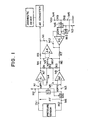
- Symbols N1 through N16 indicate nodes respectively.
- Symbols A1 through A4 indicate Operational Amplifiers (hereinafter called “Op amps”) respectively.
- Symbols S1 through S4 designate analog switches respectively.
- Symbols R1 through R8 indicate resistors respectively.
- Symbol R9 designate a variable resistor.
- One of output terminals of a pressure sensor is electrically connected to an input terminal IN1, whereas the other thereof is electrically connected to an input terminal IN2.
- the node N1 is electrically connected to the input terminal IN1, a positive input (hereinafter called “non-inverting input”) of the Op amp A1 and one analog input/output of the analog switch S1.
- the node N2 is electrically connected to control inputs of the analog switches S1, S2, S3 and S4.
- the node N3 is electrically connected to one analog input/output of the analog switch S2 and a non-inverting input of the Op amp A2.
- the node N4 is electrically connected to a negative input (hereinafter called "inverting input") of the Op amp A1, one end of the resistor R1 and one end of the resistor R2.
- the node N5 is electrically connected to an inverting input of the Op amp A2, one end of the resistor R3 and the other end of the resistor R2.
- the node N6 is electrically connected to the input terminal IN2 and the other analog input/output of the analog switch S2.
- the node N7 is electrically connected to the output of the Op amp A1, the other end of the resistor R1 and one end of the resistor R4.
- the node N8 is electrically connected to the output of the Op amp A2, the other end of the resistor R3 and one end of the resistor R6.
- the node N9 is electrically connected to the other end of the resistor R4, one end of the resistor R5 and an inverting input of the Op amp A4.
- the node N10 is electrically connected to the other end of the resistor R6, one end of the resistor R7 and a non-inverting input of the Op amp A4.
- the node N11 is electrically connected to the output of the Op amp A4, the other end of the resistor R5 and the input of an Analog Digital converter (hereinafter called "AD converter").
- the node N12 is electrically connected to the other end of the resistor R7, the output of the Op amp A3 and an inverting input of the Op amp A3.
- the node N13 is electrically connected to a non-inverting input of the Op amp A3, one analog input/output of the analog switch S3 and one analog input/output of the analog switch S4.
- the node N16 is electrically connected to the other analog input/output of the analog switch S3, one end of the resistor R8 and one end of the resistor R9.
- the node N14 is electrically connected to the other end of the resistor R9.
- the node N14 is supplied with a source potential VDD.
- the node N15 is electrically connected to the other end of the resistor R8 and the other analog input/output of the analog switch S4.
- the node N15 is supplied with a ground potential GND.
- a preamplifier unit is composed of the analog switches S1 and S2, the Op amps A1 and A2 and the resistors R1 through R3.
- a level shifting unit is composed of the analog switches S3 and S4, the Op amps A3 and A4, the resistors R4 through R8 and the variable resistor R9.
- the ratio among resistance values of the resistors R1, R2, R3 and R4 will be defined as 1 : 1 : 1 : 1.
- variable resistor R9 serves so as to adjust a potential level at the node N16 and adjust a potential level at the node N13 when the analog switch S3 is turned on.
- the offset cancel circuit according to the first embodiment has two states of an input potential difference measurement mode and an offset measurement mode.
- the node N2 is set to an L level.
- the switches S1 and S4 are turned OFF and the switches S2 and S3 are turned ON.
- a predetermined pressure is applied to the pressure sensor so that a potential difference ⁇ V is outputted.
- the preamplifier unit amplifies the potential difference ⁇ V by (R1 + R2 + R3)/R2 times.
- the level shifting unit supplies a potential VN11 that meets the following relation, to the node N11 based on the amplified potential difference (R1 + R2 + R3)/R2 ⁇ V and a potential VN13 at the node N13.
- VN11 (R1 + R2 + R3)/R2 ⁇ V + VN13
- the expression 2 is of a theoretical expression at the time that it is assumed that no offset voltage appears between the non-inverting and inverting input terminals of each of the individual Op amps A1, A2, A3 and A4.
- offset voltages VOFF1, VOFF2, VOFF3 and VOFF4 respectively exist between the non-inverting and inverting input terminals of the Op amps A1, A2, A3 and A4.
- VN11 (R1 + R2 + R3)/R2 ⁇ ( ⁇ V + VOFF1 - VOFF2) + VN13 + VOFF3 + 2 ⁇ VOFF4
- Vop (R1 + R2 + R3)/R2 ⁇ (VOFF1 - VOFF2) + VOFF3 + 2 ⁇ VOFF4
- the error Vop differs according to each product.
- the VN13 can be set to a desired value.
- the VN11 can be set to the same value between products by adjusting the VN13 in advance at each product.
- the offset voltages vary according to temperatures, the source potential, etc.
- the output potential VN11 varies according to the state of usage of a single product even in the case of the single product.
- the pressure sensor also has an offset voltage.
- an error occurs even in the potential difference ⁇ V produced from the pressure sensor and the potential difference ⁇ V is shifted from an ideal value.
- d an ideal potential difference supplied between the input terminals IN1 and IN2
- e an output potential difference error caused by the offset voltage of the pressure sensor
- Vp (R1 + R2 + R3)/R2 ⁇ e
- the offset measurement mode is set to the offset cancel circuit.
- the AD converter is supplied with the VN11 and performs AD conversion on the VN11.
- the AD converter outputs a value based on the VN11 to an arithmetic device.
- the AD converter is inputted with the VN11' and performs AD conversion on the VN11'.
- the AD converter outputs a value based on the VN11' to the arithmetic device.
- the arithmetic device computes the difference between the two values outputted from the AD converter. For simplicity of illustration, the following description will be made on the assumption that an input ahead of its AD conversion and an output obtained after its AD conversion are equal to each other.
- VN11 - VN11' (R1 + R2 + R3)/R2 ⁇ V + VN13
- VN11 - VN11' (R1 + R2 R3)/R2 ⁇ (d + e) + VN13
- Vp (R1 + R2 + R3)/R2 ⁇ e
- the offset voltage of the pressure sensor varies under the influence of temperatures and a source potential.
- the influence of the output potential difference error e developed due to the offset voltage of the pressure sensor on the temperatures and the source potential is known in advance.
- a change in output potential VN11 due to their variations can be calculated by the arithmetic device. Therefore, such a change can be canceled.
- the difference VN11 - VN11' can be equally set between products by setting the VN13 to a desired value at each product. Namely, a shift in the error e at each product produced due to the offset voltage of the pressure sensor can be canceled.
- the potential at the node N13 is switched between the input potential difference measurement mode and the offset voltage measurement mode.
- the term of VN13 appears in the expression 5 indicative of the difference between the value (expression 3) measured under the input potential difference measurement mode and the value (expression 4) measured under the offset voltage measurement mode. Therefore, the difference VN11 - VN11' can be set to a given value by adjusting and shifting the VN13 to the desired value at each product. As a result, the influence of the offset voltages of the Op amps and the shift developed at each product due to the offset voltage of the pressure sensor can be eliminated.
- Fig. 2 is a circuit diagram showing an offset cancel system according to a second embodiment of the present invention.
- the analog switch S3 shown in Fig. 1 is omitted from the offset cancel system shown in Fig. 2.
- a node N13 is electrically connected to a non-inverting input of an Op amp A3 and one ends of resistors R8 and R9.
- a node N14 is electrically connected to the other end of the resistor R9 and a source potential VDD.
- a node N15 is electrically connected to the other end of the resistor R8, one analog input/output of an analog switch S4 and a ground potential GND.
- a node N12 is electrically connected to the other analog input/output of the analog switch S4, the output of the Op amp A3, an inverting input of the Op amp A3 and one terminal of a resistor R7.
- a control input of the analog switch S4 is electrically connected to a node N2.
- An output enable input OE of the Op amp A3 is electrically connected to the node N2.
- VN11 - VN11' (R1 + R2 + R3)/R2 ⁇ V + VOFF3 + VN16 - VN15
- VN11 - VN11' (R1 + R2 + R3)/R2 ⁇ V + VOFF3 + VN16 - VN15
- the term of the error produced by the offset voltage of the Op amp A3 is left on the above expression. Since, however, the Op amp A3 is disabled when the second embodiment is placed in the offset measurement mode, an advantage can be brought about that the current to be consumed by the Op amp A3 can be set to zero.
Landscapes
- Physics & Mathematics (AREA)
- General Physics & Mathematics (AREA)
- Engineering & Computer Science (AREA)
- Technology Law (AREA)
- Amplifiers (AREA)
- Measurement Of Current Or Voltage (AREA)
- Measuring Fluid Pressure (AREA)
- Testing Or Calibration Of Command Recording Devices (AREA)
Applications Claiming Priority (3)
| Application Number | Priority Date | Filing Date | Title |
|---|---|---|---|
| JP14625295A JP3609152B2 (ja) | 1995-06-13 | 1995-06-13 | オフセットキャンセル回路とそれを用いたオフセットキャンセルシステム |
| JP14625295 | 1995-06-13 | ||
| JP146252/95 | 1995-06-13 |
Publications (2)
| Publication Number | Publication Date |
|---|---|
| EP0749001A1 EP0749001A1 (en) | 1996-12-18 |
| EP0749001B1 true EP0749001B1 (en) | 2000-09-06 |
Family
ID=15403545
Family Applications (1)
| Application Number | Title | Priority Date | Filing Date |
|---|---|---|---|
| EP96109526A Expired - Lifetime EP0749001B1 (en) | 1995-06-13 | 1996-06-13 | Offset cancel circuit and offset cancel method using the same |
Country Status (6)
| Country | Link |
|---|---|
| US (1) | US5703516A (cg-RX-API-DMAC7.html) |
| EP (1) | EP0749001B1 (cg-RX-API-DMAC7.html) |
| JP (1) | JP3609152B2 (cg-RX-API-DMAC7.html) |
| CN (1) | CN1062393C (cg-RX-API-DMAC7.html) |
| DE (1) | DE69610160T2 (cg-RX-API-DMAC7.html) |
| TW (1) | TW310387B (cg-RX-API-DMAC7.html) |
Families Citing this family (7)
| Publication number | Priority date | Publication date | Assignee | Title |
|---|---|---|---|---|
| US6194965B1 (en) * | 1999-09-03 | 2001-02-27 | Cypress Semiconductor Corp. | Differential signal detection circuit |
| JP4515241B2 (ja) * | 2004-12-16 | 2010-07-28 | Okiセミコンダクタ株式会社 | 出力増幅回路及びそれを用いたセンサ装置 |
| US7522676B2 (en) * | 2006-02-06 | 2009-04-21 | Nokia Corporation | Method and system for transmitter envelope delay calibration |
| DE102006045893A1 (de) * | 2006-09-28 | 2008-04-03 | Siemens Ag | Automatische Verschiebung des Messwerterfassungsbereichs einer sensorischen Messeinrichtung |
| JP2008312079A (ja) * | 2007-06-18 | 2008-12-25 | Denso Corp | 増幅回路 |
| CN102612279A (zh) * | 2011-01-19 | 2012-07-25 | 鸿富锦精密工业(深圳)有限公司 | 服务器机柜 |
| CN116558679A (zh) * | 2023-05-11 | 2023-08-08 | 上海泰矽微电子有限公司 | 偏压消除电路和压力测量电路 |
Family Cites Families (7)
| Publication number | Priority date | Publication date | Assignee | Title |
|---|---|---|---|---|
| US4521702A (en) * | 1982-10-13 | 1985-06-04 | The United States Of America As Represented By The Administrator, National Aeronautics And Space Administration | Reactanceless synthesized impedance bandpass amplifier |
| JP2534520B2 (ja) * | 1987-11-13 | 1996-09-18 | シチズン時計株式会社 | 生体組織張力計 |
| GB2234069B (en) * | 1988-10-28 | 1992-08-12 | Motorola Inc | Sensor arrangement |
| US5047665A (en) * | 1989-02-08 | 1991-09-10 | Burr-Brown Corporation | Low noise, low offset, high speed CMOS differential amplifier |
| US5032740A (en) * | 1989-11-06 | 1991-07-16 | Eastman Kodak Company | Voltage level conversion of a clock signal |
| JP2625347B2 (ja) * | 1993-04-20 | 1997-07-02 | 日本電気株式会社 | ディジタル受信器の自動オフセット制御回路 |
| US5327099A (en) * | 1993-08-02 | 1994-07-05 | Motorola, Inc. | Differential stage that provides minimal offset between inputs |
-
1995
- 1995-06-13 JP JP14625295A patent/JP3609152B2/ja not_active Expired - Fee Related
-
1996
- 1996-03-27 US US08/623,901 patent/US5703516A/en not_active Expired - Lifetime
- 1996-03-27 TW TW085103699A patent/TW310387B/zh active
- 1996-06-10 CN CN96107646A patent/CN1062393C/zh not_active Expired - Fee Related
- 1996-06-13 EP EP96109526A patent/EP0749001B1/en not_active Expired - Lifetime
- 1996-06-13 DE DE69610160T patent/DE69610160T2/de not_active Expired - Fee Related
Also Published As
| Publication number | Publication date |
|---|---|
| EP0749001A1 (en) | 1996-12-18 |
| CN1062393C (zh) | 2001-02-21 |
| DE69610160T2 (de) | 2001-05-10 |
| US5703516A (en) | 1997-12-30 |
| JP3609152B2 (ja) | 2005-01-12 |
| JPH08340222A (ja) | 1996-12-24 |
| DE69610160D1 (de) | 2000-10-12 |
| TW310387B (cg-RX-API-DMAC7.html) | 1997-07-11 |
| CN1141532A (zh) | 1997-01-29 |
Similar Documents
| Publication | Publication Date | Title |
|---|---|---|
| US5469071A (en) | Resistor sensor input apparatus | |
| EP0409213A2 (en) | Amplifiying compensation circuit for semiconductor pressure sensor | |
| JP2928526B2 (ja) | 電源回路及び前記回路を備えるブリッジ型測定器出力補償回路 | |
| EP0749001B1 (en) | Offset cancel circuit and offset cancel method using the same | |
| US5532582A (en) | Analog input apparatus | |
| JP4642413B2 (ja) | 電流検出装置 | |
| JP3244212B2 (ja) | ディジタル測定器 | |
| US6765391B2 (en) | Low cost asic architecture for safety critical applications monitoring an applied stimulus | |
| JPH08327677A (ja) | 容量型センサ用検出回路および検出方法 | |
| JP2000214029A (ja) | 圧力センサ回路 | |
| JP4617545B2 (ja) | センサの異常検出回路及び物理量検出装置 | |
| JP3584803B2 (ja) | 圧力センサ回路 | |
| JP4272267B2 (ja) | 静電容量型センサ回路 | |
| JP2009121934A (ja) | 温度補正装置及び温度補正方法 | |
| CN100480660C (zh) | 电阻型热损失的压力感应器及操作方法 | |
| JPH11160347A (ja) | センサ回路 | |
| JP2002084151A (ja) | 物理量検出装置 | |
| KR19980076201A (ko) | 측온저항소자를 이용한 온도측정장치 | |
| JPH11183273A (ja) | センサの温度補償回路 | |
| JP2000214030A (ja) | 圧力センサ回路 | |
| JP2006170797A (ja) | 不平衝容量の検出装置、及びセンサの不平衝容量の検出方法、並びにこれらに用いる変換器 | |
| JP2595858B2 (ja) | 温度測定回路 | |
| JP4050813B2 (ja) | トランスミッタ | |
| JPWO2022023915A5 (cg-RX-API-DMAC7.html) | ||
| JPH02206730A (ja) | 自己診断回路 |
Legal Events
| Date | Code | Title | Description |
|---|---|---|---|
| PUAI | Public reference made under article 153(3) epc to a published international application that has entered the european phase |
Free format text: ORIGINAL CODE: 0009012 |
|
| AK | Designated contracting states |
Kind code of ref document: A1 Designated state(s): CH DE GB LI |
|
| 17P | Request for examination filed |
Effective date: 19970616 |
|
| 17Q | First examination report despatched |
Effective date: 19970903 |
|
| RTI1 | Title (correction) |
Free format text: OFFSET CANCEL CIRCUIT AND OFFSET CANCEL METHOD USING THE SAME |
|
| GRAG | Despatch of communication of intention to grant |
Free format text: ORIGINAL CODE: EPIDOS AGRA |
|
| GRAG | Despatch of communication of intention to grant |
Free format text: ORIGINAL CODE: EPIDOS AGRA |
|
| GRAH | Despatch of communication of intention to grant a patent |
Free format text: ORIGINAL CODE: EPIDOS IGRA |
|
| GRAH | Despatch of communication of intention to grant a patent |
Free format text: ORIGINAL CODE: EPIDOS IGRA |
|
| GRAA | (expected) grant |
Free format text: ORIGINAL CODE: 0009210 |
|
| AK | Designated contracting states |
Kind code of ref document: B1 Designated state(s): CH DE GB LI |
|
| REG | Reference to a national code |
Ref country code: CH Ref legal event code: EP |
|
| REF | Corresponds to: |
Ref document number: 69610160 Country of ref document: DE Date of ref document: 20001012 |
|
| REG | Reference to a national code |
Ref country code: CH Ref legal event code: NV Representative=s name: SCHMAUDER & PARTNER AG PATENTANWALTSBUERO |
|
| EN | Fr: translation not filed | ||
| PLBE | No opposition filed within time limit |
Free format text: ORIGINAL CODE: 0009261 |
|
| STAA | Information on the status of an ep patent application or granted ep patent |
Free format text: STATUS: NO OPPOSITION FILED WITHIN TIME LIMIT |
|
| 26N | No opposition filed | ||
| REG | Reference to a national code |
Ref country code: GB Ref legal event code: IF02 |
|
| REG | Reference to a national code |
Ref country code: GB Ref legal event code: 732E Free format text: REGISTERED BETWEEN 20090416 AND 20090422 |
|
| REG | Reference to a national code |
Ref country code: CH Ref legal event code: PCAR Free format text: SCHMAUDER & PARTNER AG PATENT- UND MARKENANWAELTE VSP;ZWAENGIWEG 7;8038 ZUERICH (CH) |
|
| PGFP | Annual fee paid to national office [announced via postgrant information from national office to epo] |
Ref country code: CH Payment date: 20090615 Year of fee payment: 14 |
|
| PGFP | Annual fee paid to national office [announced via postgrant information from national office to epo] |
Ref country code: GB Payment date: 20090610 Year of fee payment: 14 Ref country code: DE Payment date: 20090615 Year of fee payment: 14 |
|
| REG | Reference to a national code |
Ref country code: CH Ref legal event code: PL |
|
| GBPC | Gb: european patent ceased through non-payment of renewal fee |
Effective date: 20100613 |
|
| PG25 | Lapsed in a contracting state [announced via postgrant information from national office to epo] |
Ref country code: DE Free format text: LAPSE BECAUSE OF NON-PAYMENT OF DUE FEES Effective date: 20110101 Ref country code: CH Free format text: LAPSE BECAUSE OF NON-PAYMENT OF DUE FEES Effective date: 20100630 Ref country code: LI Free format text: LAPSE BECAUSE OF NON-PAYMENT OF DUE FEES Effective date: 20100630 |
|
| PG25 | Lapsed in a contracting state [announced via postgrant information from national office to epo] |
Ref country code: GB Free format text: LAPSE BECAUSE OF NON-PAYMENT OF DUE FEES Effective date: 20100613 |