EP0721189A2 - Mémoire ferro-électrique et méthode de commande pour son opération - Google Patents
Mémoire ferro-électrique et méthode de commande pour son opération Download PDFInfo
- Publication number
- EP0721189A2 EP0721189A2 EP96100075A EP96100075A EP0721189A2 EP 0721189 A2 EP0721189 A2 EP 0721189A2 EP 96100075 A EP96100075 A EP 96100075A EP 96100075 A EP96100075 A EP 96100075A EP 0721189 A2 EP0721189 A2 EP 0721189A2
- Authority
- EP
- European Patent Office
- Prior art keywords
- data signal
- voltage
- ferroelectric capacitor
- memory cell
- signal lines
- Prior art date
- Legal status (The legal status is an assumption and is not a legal conclusion. Google has not performed a legal analysis and makes no representation as to the accuracy of the status listed.)
- Granted
Links
- 230000015654 memory Effects 0.000 title claims abstract description 229
- 238000000034 method Methods 0.000 title claims description 22
- 239000003990 capacitor Substances 0.000 claims abstract description 133
- 230000010287 polarization Effects 0.000 claims abstract description 27
- 230000003071 parasitic effect Effects 0.000 claims description 38
- 239000000463 material Substances 0.000 claims description 12
- 238000003491 array Methods 0.000 claims description 8
- 230000005684 electric field Effects 0.000 claims description 3
- 238000010586 diagram Methods 0.000 description 11
- 230000002269 spontaneous effect Effects 0.000 description 4
- 238000010276 construction Methods 0.000 description 3
- 230000009471 action Effects 0.000 description 2
- 230000003321 amplification Effects 0.000 description 2
- 230000000295 complement effect Effects 0.000 description 2
- 230000008878 coupling Effects 0.000 description 2
- 238000010168 coupling process Methods 0.000 description 2
- 238000005859 coupling reaction Methods 0.000 description 2
- 229910052451 lead zirconate titanate Inorganic materials 0.000 description 2
- 230000007246 mechanism Effects 0.000 description 2
- 238000003199 nucleic acid amplification method Methods 0.000 description 2
- 230000007547 defect Effects 0.000 description 1
- HFGPZNIAWCZYJU-UHFFFAOYSA-N lead zirconate titanate Chemical compound [O-2].[O-2].[O-2].[O-2].[O-2].[Ti+4].[Zr+4].[Pb+2] HFGPZNIAWCZYJU-UHFFFAOYSA-N 0.000 description 1
- 238000004519 manufacturing process Methods 0.000 description 1
- 230000004048 modification Effects 0.000 description 1
- 238000012986 modification Methods 0.000 description 1
Images


Classifications
-
- G—PHYSICS
- G11—INFORMATION STORAGE
- G11C—STATIC STORES
- G11C11/00—Digital stores characterised by the use of particular electric or magnetic storage elements; Storage elements therefor
- G11C11/21—Digital stores characterised by the use of particular electric or magnetic storage elements; Storage elements therefor using electric elements
- G11C11/22—Digital stores characterised by the use of particular electric or magnetic storage elements; Storage elements therefor using electric elements using ferroelectric elements
Definitions
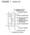
- the present invention relates to a ferroelectric memory and a method for controlling an operation thereof.
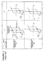
- the signal voltage VSIG defined by the equations (14) and (15) must exceed the minimum voltage value VSE which can be normally amplified by the sense amplifier. Namely, VSIG ⁇ VSE
Landscapes
- Engineering & Computer Science (AREA)
- Computer Hardware Design (AREA)
- Dram (AREA)
- Semiconductor Memories (AREA)
Applications Claiming Priority (3)
| Application Number | Priority Date | Filing Date | Title |
|---|---|---|---|
| JP07000065A JP3127751B2 (ja) | 1995-01-04 | 1995-01-04 | 強誘電体メモリ装置およびその動作制御方法 |
| JP6595 | 1995-01-04 | ||
| JP65/95 | 1995-01-04 |
Publications (3)
| Publication Number | Publication Date |
|---|---|
| EP0721189A2 true EP0721189A2 (fr) | 1996-07-10 |
| EP0721189A3 EP0721189A3 (fr) | 1999-01-27 |
| EP0721189B1 EP0721189B1 (fr) | 2002-10-09 |
Family
ID=11463797
Family Applications (1)
| Application Number | Title | Priority Date | Filing Date |
|---|---|---|---|
| EP96100075A Expired - Lifetime EP0721189B1 (fr) | 1995-01-04 | 1996-01-04 | Mémoire ferro-électrique et méthode de commande pour son opération |
Country Status (6)
| Country | Link |
|---|---|
| US (1) | US5668753A (fr) |
| EP (1) | EP0721189B1 (fr) |
| JP (1) | JP3127751B2 (fr) |
| KR (1) | KR100201734B1 (fr) |
| DE (1) | DE69624155T2 (fr) |
| TW (1) | TW290688B (fr) |
Cited By (2)
| Publication number | Priority date | Publication date | Assignee | Title |
|---|---|---|---|---|
| WO1998058383A3 (fr) * | 1997-06-17 | 1999-04-01 | Opticom As | Dispositif passif electriquement adressable, procede d'adressage electrique de celui-ci et utilisation du dispositif et mise en oeuvre du procede |
| US6498744B2 (en) | 1997-08-15 | 2002-12-24 | Thin Film Electronics Asa | Ferroelectric data processing device |
Families Citing this family (19)
| Publication number | Priority date | Publication date | Assignee | Title |
|---|---|---|---|---|
| JP3186485B2 (ja) * | 1995-01-04 | 2001-07-11 | 日本電気株式会社 | 強誘電体メモリ装置およびその動作制御方法 |
| JP3629099B2 (ja) * | 1996-06-28 | 2005-03-16 | 株式会社東芝 | 半導体記憶装置 |
| JP3758054B2 (ja) * | 1996-08-23 | 2006-03-22 | ローム株式会社 | 半導体記憶装置 |
| JPH10163451A (ja) * | 1996-12-02 | 1998-06-19 | Hitachi Ltd | 半導体記憶装置 |
| US5815431A (en) * | 1997-02-19 | 1998-09-29 | Vlsi Technology, Inc. | Non-volatile digital circuits using ferroelectric capacitors |
| US5969980A (en) * | 1997-11-14 | 1999-10-19 | Ramtron International Corporation | Sense amplifier configuration for a 1T/1C ferroelectric memory |
| US5880989A (en) * | 1997-11-14 | 1999-03-09 | Ramtron International Corporation | Sensing methodology for a 1T/1C ferroelectric memory |
| US6028783A (en) | 1997-11-14 | 2000-02-22 | Ramtron International Corporation | Memory cell configuration for a 1T/1C ferroelectric memory |
| US5978251A (en) * | 1997-11-14 | 1999-11-02 | Ramtron International Corporation | Plate line driver circuit for a 1T/1C ferroelectric memory |
| US5986919A (en) * | 1997-11-14 | 1999-11-16 | Ramtron International Corporation | Reference cell configuration for a 1T/1C ferroelectric memory |
| US5995406A (en) * | 1997-11-14 | 1999-11-30 | Ramtron International Corporation | Plate line segmentation in a 1T/1C ferroelectric memory |
| US5956266A (en) * | 1997-11-14 | 1999-09-21 | Ramtron International Corporation | Reference cell for a 1T/1C ferroelectric memory |
| US5892728A (en) * | 1997-11-14 | 1999-04-06 | Ramtron International Corporation | Column decoder configuration for a 1T/1C ferroelectric memory |
| US6002634A (en) * | 1997-11-14 | 1999-12-14 | Ramtron International Corporation | Sense amplifier latch driver circuit for a 1T/1C ferroelectric memory |
| US20050122765A1 (en) * | 1997-11-14 | 2005-06-09 | Allen Judith E. | Reference cell configuration for a 1T/1C ferroelectric memory |
| JP2002083495A (ja) * | 2000-06-30 | 2002-03-22 | Seiko Epson Corp | 半導体集積回路の情報記憶方法、半導体集積回路、その半導体集積回路を多数備えた半導体装置、及びその半導体装置を用いた電子機器 |
| KR20020007792A (ko) * | 2000-07-19 | 2002-01-29 | 박종섭 | 패키지에 따른 강유전체 메모리 소자 열화 감소 방법 |
| US9941021B2 (en) | 2016-06-16 | 2018-04-10 | Micron Technology, Inc. | Plate defect mitigation techniques |
| US10403389B2 (en) | 2016-06-16 | 2019-09-03 | Micron Technology, Inc. | Array plate short repair |
Family Cites Families (9)
| Publication number | Priority date | Publication date | Assignee | Title |
|---|---|---|---|---|
| US4873664A (en) * | 1987-02-12 | 1989-10-10 | Ramtron Corporation | Self restoring ferroelectric memory |
| US4888733A (en) * | 1988-09-12 | 1989-12-19 | Ramtron Corporation | Non-volatile memory cell and sensing method |
| JPH088339B2 (ja) * | 1988-10-19 | 1996-01-29 | 株式会社東芝 | 半導体メモリ |
| US5270967A (en) * | 1991-01-16 | 1993-12-14 | National Semiconductor Corporation | Refreshing ferroelectric capacitors |
| JPH04345992A (ja) * | 1991-05-24 | 1992-12-01 | Fujitsu Ltd | スタティックram |
| JPH05160378A (ja) * | 1991-12-10 | 1993-06-25 | Nippon Sheet Glass Co Ltd | 2次元イメージセンサ |
| KR970000870B1 (ko) * | 1992-12-02 | 1997-01-20 | 마쯔시다덴기산교 가부시기가이샤 | 반도체메모리장치 |
| US5430671A (en) * | 1993-04-09 | 1995-07-04 | Matsushita Electric Industrial Co., Ltd. | Semiconductor memory device |
| JP3186485B2 (ja) * | 1995-01-04 | 2001-07-11 | 日本電気株式会社 | 強誘電体メモリ装置およびその動作制御方法 |
-
1995
- 1995-01-04 JP JP07000065A patent/JP3127751B2/ja not_active Expired - Fee Related
- 1995-12-29 TW TW084114120A patent/TW290688B/zh active
-
1996
- 1996-01-04 US US08/582,734 patent/US5668753A/en not_active Expired - Lifetime
- 1996-01-04 DE DE69624155T patent/DE69624155T2/de not_active Expired - Fee Related
- 1996-01-04 KR KR1019960000910A patent/KR100201734B1/ko not_active Expired - Fee Related
- 1996-01-04 EP EP96100075A patent/EP0721189B1/fr not_active Expired - Lifetime
Cited By (6)
| Publication number | Priority date | Publication date | Assignee | Title |
|---|---|---|---|---|
| WO1998058383A3 (fr) * | 1997-06-17 | 1999-04-01 | Opticom As | Dispositif passif electriquement adressable, procede d'adressage electrique de celui-ci et utilisation du dispositif et mise en oeuvre du procede |
| US6055180A (en) * | 1997-06-17 | 2000-04-25 | Thin Film Electronics Asa | Electrically addressable passive device, method for electrical addressing of the same and uses of the device and the method |
| RU2182732C2 (ru) * | 1997-06-17 | 2002-05-20 | Тин Филм Электроникс Аса | Электрически адресуемое устройство, способ электрической адресации и использование этого устройства и этого способа |
| CN100440374C (zh) * | 1997-06-17 | 2008-12-03 | 薄膜电子有限公司 | 电可寻址器件,该器件电寻址的方法以及所述器件和方法的使用 |
| US6498744B2 (en) | 1997-08-15 | 2002-12-24 | Thin Film Electronics Asa | Ferroelectric data processing device |
| US6670659B1 (en) | 1997-08-15 | 2003-12-30 | Thin Film Electronics Asa | Ferroelectric data processing device |
Also Published As
| Publication number | Publication date |
|---|---|
| EP0721189A3 (fr) | 1999-01-27 |
| JP3127751B2 (ja) | 2001-01-29 |
| US5668753A (en) | 1997-09-16 |
| TW290688B (fr) | 1996-11-11 |
| JPH08185697A (ja) | 1996-07-16 |
| DE69624155D1 (de) | 2002-11-14 |
| DE69624155T2 (de) | 2003-05-28 |
| KR100201734B1 (ko) | 1999-06-15 |
| KR960030238A (ko) | 1996-08-17 |
| EP0721189B1 (fr) | 2002-10-09 |
Similar Documents
| Publication | Publication Date | Title |
|---|---|---|
| EP0721189B1 (fr) | Mémoire ferro-électrique et méthode de commande pour son opération | |
| EP0721191B1 (fr) | Mémoire ferro-électrique et méthode de commande pour son opération | |
| US5361224A (en) | Nonvolatile memory device having ferroelectric film | |
| JP3183076B2 (ja) | 強誘電体メモリ装置 | |
| US5615144A (en) | Non-volatile ferroelectric memory device with leakage preventing function | |
| JPH08329686A (ja) | 強誘電体記憶装置 | |
| JP2000076870A (ja) | 強誘電体キャパシタを備えた不揮発性dram | |
| US5517446A (en) | Nonvolatile semiconductor memory device and method for driving the same | |
| EP0627741A2 (fr) | Dispositif de mémoire à semiconducteurs | |
| US5940316A (en) | Ferroelectric memory device using a ferroelectric material and method of reading data from the ferroelectric memory device | |
| US7142444B2 (en) | Data reading method, data writing method, and semiconductor memory device | |
| JP3604576B2 (ja) | 強誘電体メモリ装置 | |
| JPH1069789A (ja) | 強誘電体半導体メモリ装置のインプリント補償方法及び回路 | |
| EP0944092A2 (fr) | Dispositif de mémoire non volatile à semiconducteurs | |
| JP3717097B2 (ja) | 強誘電体メモリ | |
| US5610852A (en) | Ferroelectric memory and method for controlling operation of the same | |
| KR100268947B1 (ko) | 비휘발성 강유전체 메모리 및 그의 제어회로 | |
| JP4030076B2 (ja) | 処理機能付記憶装置 | |
| US6498743B2 (en) | Method for supplying reference potential to sense amplifier circuit in semiconductor integrated circuit, semiconductor integrated circuit, semiconductor device equipped with many of the semiconductor integrated circuits, and electronic apparatus using the semiconductor device | |
| US6885597B2 (en) | Sensing test circuit | |
| JP3441154B2 (ja) | 半導体記憶装置 | |
| JP3568876B2 (ja) | 集積メモリおよびメモリに対する作動方法 | |
| JP2861925B2 (ja) | 強誘電体メモリ装置 | |
| KR100294645B1 (ko) | 강유전체기억소자 | |
| JP2001118384A (ja) | 強誘電体メモリ |
Legal Events
| Date | Code | Title | Description |
|---|---|---|---|
| PUAI | Public reference made under article 153(3) epc to a published international application that has entered the european phase |
Free format text: ORIGINAL CODE: 0009012 |
|
| AK | Designated contracting states |
Kind code of ref document: A2 Designated state(s): DE FR GB NL |
|
| PUAL | Search report despatched |
Free format text: ORIGINAL CODE: 0009013 |
|
| AK | Designated contracting states |
Kind code of ref document: A3 Designated state(s): DE FR GB NL |
|
| 17P | Request for examination filed |
Effective date: 19990309 |
|
| 17Q | First examination report despatched |
Effective date: 19991214 |
|
| GRAG | Despatch of communication of intention to grant |
Free format text: ORIGINAL CODE: EPIDOS AGRA |
|
| GRAG | Despatch of communication of intention to grant |
Free format text: ORIGINAL CODE: EPIDOS AGRA |
|
| GRAH | Despatch of communication of intention to grant a patent |
Free format text: ORIGINAL CODE: EPIDOS IGRA |
|
| GRAH | Despatch of communication of intention to grant a patent |
Free format text: ORIGINAL CODE: EPIDOS IGRA |
|
| GRAA | (expected) grant |
Free format text: ORIGINAL CODE: 0009210 |
|
| AK | Designated contracting states |
Kind code of ref document: B1 Designated state(s): DE FR GB NL |
|
| PG25 | Lapsed in a contracting state [announced via postgrant information from national office to epo] |
Ref country code: NL Free format text: LAPSE BECAUSE OF FAILURE TO SUBMIT A TRANSLATION OF THE DESCRIPTION OR TO PAY THE FEE WITHIN THE PRESCRIBED TIME-LIMIT Effective date: 20021009 |
|
| REG | Reference to a national code |
Ref country code: GB Ref legal event code: FG4D |
|
| REF | Corresponds to: |
Ref document number: 69624155 Country of ref document: DE Date of ref document: 20021114 |
|
| NLV1 | Nl: lapsed or annulled due to failure to fulfill the requirements of art. 29p and 29m of the patents act | ||
| ET | Fr: translation filed | ||
| RAP2 | Party data changed (patent owner data changed or rights of a patent transferred) |
Owner name: NEC ELECTRONICS CORPORATION |
|
| REG | Reference to a national code |
Ref country code: GB Ref legal event code: 732E |
|
| PLBE | No opposition filed within time limit |
Free format text: ORIGINAL CODE: 0009261 |
|
| STAA | Information on the status of an ep patent application or granted ep patent |
Free format text: STATUS: NO OPPOSITION FILED WITHIN TIME LIMIT |
|
| 26N | No opposition filed |
Effective date: 20030710 |
|
| REG | Reference to a national code |
Ref country code: FR Ref legal event code: TP |
|
| PGFP | Annual fee paid to national office [announced via postgrant information from national office to epo] |
Ref country code: GB Payment date: 20031231 Year of fee payment: 9 |
|
| PGFP | Annual fee paid to national office [announced via postgrant information from national office to epo] |
Ref country code: FR Payment date: 20040108 Year of fee payment: 9 |
|
| PGFP | Annual fee paid to national office [announced via postgrant information from national office to epo] |
Ref country code: DE Payment date: 20040115 Year of fee payment: 9 |
|
| PG25 | Lapsed in a contracting state [announced via postgrant information from national office to epo] |
Ref country code: GB Free format text: LAPSE BECAUSE OF NON-PAYMENT OF DUE FEES Effective date: 20050104 |
|
| PG25 | Lapsed in a contracting state [announced via postgrant information from national office to epo] |
Ref country code: DE Free format text: LAPSE BECAUSE OF NON-PAYMENT OF DUE FEES Effective date: 20050802 |
|
| GBPC | Gb: european patent ceased through non-payment of renewal fee |
Effective date: 20050104 |
|
| PG25 | Lapsed in a contracting state [announced via postgrant information from national office to epo] |
Ref country code: FR Free format text: LAPSE BECAUSE OF NON-PAYMENT OF DUE FEES Effective date: 20050930 |
|
| REG | Reference to a national code |
Ref country code: FR Ref legal event code: ST |