EP0712137A2 - Mémoire à semi-conducteurs programmable - Google Patents
Mémoire à semi-conducteurs programmable Download PDFInfo
- Publication number
- EP0712137A2 EP0712137A2 EP95117664A EP95117664A EP0712137A2 EP 0712137 A2 EP0712137 A2 EP 0712137A2 EP 95117664 A EP95117664 A EP 95117664A EP 95117664 A EP95117664 A EP 95117664A EP 0712137 A2 EP0712137 A2 EP 0712137A2
- Authority
- EP
- European Patent Office
- Prior art keywords
- zone
- transistor
- voltage
- melting zone
- drain
- Prior art date
- Legal status (The legal status is an assumption and is not a legal conclusion. Google has not performed a legal analysis and makes no representation as to the accuracy of the status listed.)
- Granted
Links
Images
Classifications
-
- G—PHYSICS
- G11—INFORMATION STORAGE
- G11C—STATIC STORES
- G11C17/00—Read-only memories programmable only once; Semi-permanent stores, e.g. manually-replaceable information cards
- G11C17/14—Read-only memories programmable only once; Semi-permanent stores, e.g. manually-replaceable information cards in which contents are determined by selectively establishing, breaking or modifying connecting links by permanently altering the state of coupling elements, e.g. PROM
- G11C17/16—Read-only memories programmable only once; Semi-permanent stores, e.g. manually-replaceable information cards in which contents are determined by selectively establishing, breaking or modifying connecting links by permanently altering the state of coupling elements, e.g. PROM using electrically-fusible links
-
- H—ELECTRICITY
- H01—ELECTRIC ELEMENTS
- H01L—SEMICONDUCTOR DEVICES NOT COVERED BY CLASS H10
- H01L23/00—Details of semiconductor or other solid state devices
- H01L23/52—Arrangements for conducting electric current within the device in operation from one component to another, i.e. interconnections, e.g. wires, lead frames
- H01L23/522—Arrangements for conducting electric current within the device in operation from one component to another, i.e. interconnections, e.g. wires, lead frames including external interconnections consisting of a multilayer structure of conductive and insulating layers inseparably formed on the semiconductor body
- H01L23/525—Arrangements for conducting electric current within the device in operation from one component to another, i.e. interconnections, e.g. wires, lead frames including external interconnections consisting of a multilayer structure of conductive and insulating layers inseparably formed on the semiconductor body with adaptable interconnections
- H01L23/5252—Arrangements for conducting electric current within the device in operation from one component to another, i.e. interconnections, e.g. wires, lead frames including external interconnections consisting of a multilayer structure of conductive and insulating layers inseparably formed on the semiconductor body with adaptable interconnections comprising anti-fuses, i.e. connections having their state changed from non-conductive to conductive
-
- H—ELECTRICITY
- H01—ELECTRIC ELEMENTS
- H01L—SEMICONDUCTOR DEVICES NOT COVERED BY CLASS H10
- H01L2924/00—Indexing scheme for arrangements or methods for connecting or disconnecting semiconductor or solid-state bodies as covered by H01L24/00
- H01L2924/0001—Technical content checked by a classifier
- H01L2924/0002—Not covered by any one of groups H01L24/00, H01L24/00 and H01L2224/00
-
- H—ELECTRICITY
- H01—ELECTRIC ELEMENTS
- H01L—SEMICONDUCTOR DEVICES NOT COVERED BY CLASS H10
- H01L2924/00—Indexing scheme for arrangements or methods for connecting or disconnecting semiconductor or solid-state bodies as covered by H01L24/00
- H01L2924/30—Technical effects
- H01L2924/301—Electrical effects
- H01L2924/3011—Impedance
Definitions
- the invention relates to a programmable semiconductor memory.
- an EPROM can be used as a programmable memory.
- the disadvantage of using an EPROM is that the manufacturing process is relatively complicated and expensive and that the space required for such a circuit is relatively large.
- a programmable semiconductor arrangement with programmable elements is known from WO 92/20095.
- These programmable elements can have an anti-melting zone.
- Such an anti-melting zone consists of a material which does not conduct electricity in a first state, the non-programmed and high-resistance state, and in a second state, the programmed and low-resistance state, which is generated by applying a sufficiently high voltage.
- the anti-melting zone is used in this invention to establish an electrical short circuit between two conductive paths by applying an external voltage.
- the invention has for its object to provide a programmable semiconductor memory that can be produced in a MOS process with little effort and takes up little space.
- a programmable semiconductor memory with a MOS field-effect transistor between the gate electrode and the drain zone of which an anti-melting zone is provided, which isolates the gate electrode and the drain zone from one another before the application of a programming voltage, and by applying the programming voltage which is greater than the operating voltage is in its low-resistance state and thus represents a conductive connection between the gate electrode and the drain zone.
- the transistor is programmable due to the anti-melting zone and forms its base cell. Programming is done by applying the programming voltage.
- the base cell or the transistor can be read out by applying a voltage which is greater than the transistor voltage. If the transistor is programmed, there is a low-resistance connection between the gate electrode and the drain connection of the transistor because of the low-resistance anti-melting zone in this state. In this case, a current can flow through the transistor and be detected. If the base cell or the transistor is not programmed, the gate electrode is isolated from the drain connection by the anti-melting zone which is insulating in this state, so that no current can flow through the transistor.
- the anti-melting zone Due to the arrangement of the anti-melting zone between the gate electrode and the drain zone of the transistor, a space-saving arrangement is achieved. Furthermore, the anti-melt zone can be made using only one additional mask in the MOS process. Thus, the effort in the manufacturing process is low.
- the semiconductor memory according to the invention can also be used in the arrangement of a plurality of programmable memories in the form of a field.
- the anti-melting zone consists of silicon dioxide. With this material, the breakdown strength with respect to an applied electrical voltage can be set within certain limits by a suitable implantation in the zone below the anti-melting zone, here the drain zone. If the anti-melting zone covers the drain zone, the breakdown strength of the anti-melting zone can be adjusted uniformly over its entire area by doping the drain zone. If the anti-melting zone is congruent with the drain zone, only an additional mask is required to produce the anti-melting zone. This considerably simplifies the manufacturing process of the semiconductor memory and makes it less expensive.
- the anti-melting zone is advantageously thinner than the gate oxide of the transistor. Then the anti-melting zone can be formed from the same material as the gate oxide. In the production process, the entire surface area of the gate oxide can then already be covered with the material of the anti-melting zone. For the thicker gate oxide, the material is additionally applied outside the area of the anti-melting zone. By applying the programming voltage to the anti-melting zone, this is converted into its low-resistance state, whereas the gate oxide maintains its insulating state due to its greater thickness. With the thickness of the anti-melting zone, the resistance to breakage thereof with respect to the voltage applied from the outside can be determined. With increasing thickness of the anti-melting zone, the breakdown strength and thus the required programming voltage increase. An advantageous thickness of the anti-melting zone is between 8 and 12 nm.
- the predetermined dielectric strength the anti-melting zone with the doping of the drain zone is less than the doping of the source zone.
- the doping can typically differ by a factor of 10. This prevents the gate oxide from breaking through due to the high doping of the source zone when the programming voltage is applied.
- a typical implant dose for the drain zone in a silicon substrate would be, for example, (2 - 10) x1014 A / cm2 when using arsenic as a dopant. The exact size also depends on the implantation energy of the respective implant material. With a thickness of the anti-melting zone made of silicon dioxide between 8 to 12 nm and with a corresponding doping, the programming voltage can be selected between 10 and 12 V for currents of 1 ⁇ A.
- the programmable semiconductor memory according to the invention can advantageously be used in an integrated circuit arrangement (IC).
- the memories can be arranged in the form of a matrix, the programming voltage and a reading voltage being able to be supplied to the memories in rows or rows.
- Each individual memory can be programmed or read out by applying the programming voltage or a reading voltage.
- a counter-voltage which prevents programming can be applied to the memories which are not currently to be programmed. This means that each memory can be programmed individually without having to program neighboring memories via a connecting line.
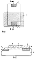
- a programmable semiconductor memory according to the invention is shown schematically. It is a transistor which has a source zone 1, a drain zone 2 and a gate electrode 3. It is assumed that this transistor is an n-channel transistor whose substrate 4 is p-doped and whose source zone 1 and drain zone 2 are n-doped. However, this does not mean any restriction of the invention, since the invention is also applicable to a p-channel transistor.
- An anti-melting zone 5 is arranged between the drain zone 2 and the gate electrode 3. Adjacent to the anti-melting zone 5, a gate oxide 6 extends between the gate electrode 3 and the substrate 4.
- the anti-melting zone 5 consists of a material which, prior to the application of a programming voltage which is greater than the operating voltage, is high-resistance and insulates the drain zone from the gate electrode .
- the programming voltage is applied via the drain zone 2 and the gate electrode 3, the anti-melting zone 5 is converted into its low-resistance state. This creates an electrically conductive connection between the drain zone 2 and the gate electrode 3.
- the transistor can therefore be programmed by applying the programming voltage so that it forms a semiconductor memory. By applying a read voltage it can be determined whether this transistor has been programmed or not. Became the transistor programmed, there is a conductive connection between the drain zone 2 and the gate electrode 3 due to the low-resistance state of the anti-melting zone 5. When the reading voltage is applied, a current then flows through the transistor, which can be detected. If the transistor has not been programmed, the drain zone is isolated from the gate electrode and no current flows through the transistor when the read voltage is applied.
- the breakdown strength of the anti-melting zone 5 can be influenced by the doping of the drain zone 2. The higher the doping of the drain zone 2, the lower the breakdown strength of the anti-melt zone 5. Another measure of the breakdown strength of the anti-melt zone 5 is its thickness. This is generally lower than the thickness of the gate oxide 6. Because the gate oxide can thus consist of the same material as the anti-melting zone 5, e.g. made of silicon dioxide. By applying the programming voltage to the drain zone 2 and the gate electrode 3 the breakthrough of the anti-melting zone 5 is then achieved, but at the same time it is ensured that the gate oxide 6 does not break through but maintains its insulating state.
- Typical values for which the memory function of the transistor are well fulfilled are 8 to 12 nm for the thickness of the anti-melting zone when using silicon dioxide, an implantation of 1014 A / cm2 and a programming voltage of 10 to 12 V at a current of one uA .
- the memory according to the invention can also be implemented with other combinations of these parameters.
- the doping of the drain zone 2 is an order of magnitude less than the doping of the source zone 1. This prevents undesired breaking through of the thin anti-melting zone 5 due to excessive doping.
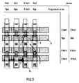
- Fig. 3 is a possible arrangement of four by four Programmable semiconductor memories according to the invention shown.
- Voltage values for programming and reading a selected transistor 7 are shown.
- the programming voltage or the reading voltage is fed in rows or columns via metal tracks.
- a line voltage 8pp is supplied to the electrode of a line 8, which is then applied to the gate electrode 3 of the transistor 7.
- a voltage of 0 V is supplied to the drain zone 2 of the transistor 7 via the column 9 via the source zone 1. Due to the programming voltage Vpp, the anti-melting zone 5 of the transistor 7 changes into its low-resistance state, so that there is a conductive connection between the drain zone 2 and the gate electrode 3.
- a current through the transistor 7 can be measured. This can be measured on line 8 or 9.
- the programming voltages Vpp applied to the other transistors prevent one of these surrounding transistors from being programmed when the transistor 7 is programmed.
- a voltage of 0 V is applied to all of these surrounding transistors at their gate electrodes and the read voltage Vdd at their source zone, so that only the current flow through the selected transistor is queried. If a voltage of OV is applied to the source zone, the transistor 7 can be read out via the column 9. At the same time, the transistors in the same row can be read out via the associated columns.
Applications Claiming Priority (2)
| Application Number | Priority Date | Filing Date | Title |
|---|---|---|---|
| DE4440539 | 1994-11-12 | ||
| DE4440539A DE4440539C2 (de) | 1994-11-12 | 1994-11-12 | Programmierbarer Halbleiterspeicher |
Publications (3)
| Publication Number | Publication Date |
|---|---|
| EP0712137A2 true EP0712137A2 (fr) | 1996-05-15 |
| EP0712137A3 EP0712137A3 (fr) | 1998-05-20 |
| EP0712137B1 EP0712137B1 (fr) | 2001-10-04 |
Family
ID=6533214
Family Applications (1)
| Application Number | Title | Priority Date | Filing Date |
|---|---|---|---|
| EP95117664A Expired - Lifetime EP0712137B1 (fr) | 1994-11-12 | 1995-11-09 | Mémoire à semi-conducteurs programmable |
Country Status (5)
| Country | Link |
|---|---|
| US (1) | US5646438A (fr) |
| EP (1) | EP0712137B1 (fr) |
| JP (1) | JPH08213483A (fr) |
| KR (1) | KR960019747A (fr) |
| DE (2) | DE4440539C2 (fr) |
Cited By (4)
| Publication number | Priority date | Publication date | Assignee | Title |
|---|---|---|---|---|
| FR2770019A1 (fr) * | 1997-10-20 | 1999-04-23 | Sgs Thomson Microelectronics | Point memoire mos |
| US6020777A (en) * | 1997-09-26 | 2000-02-01 | International Business Machines Corporation | Electrically programmable anti-fuse circuit |
| CN102612717A (zh) * | 2009-10-30 | 2012-07-25 | 赛鼎矽公司 | 双阱沟道分裂otp存储单元 |
| US11467115B2 (en) | 2017-09-27 | 2022-10-11 | Fraunhofer-Gesellschaft zur Förderung der angewandten Forschung e.V. | Fluid sensor |
Families Citing this family (25)
| Publication number | Priority date | Publication date | Assignee | Title |
|---|---|---|---|---|
| GB9600384D0 (en) * | 1996-01-09 | 1996-03-13 | Nyfotek As | Dna glycosylases |
| US5909049A (en) | 1997-02-11 | 1999-06-01 | Actel Corporation | Antifuse programmed PROM cell |
| US6229733B1 (en) | 1999-03-24 | 2001-05-08 | Texas Instruments Incorporated | Non-volatile memory cell for linear mos integrated circuits utilizing fused mosfet gate oxide |
| US6525955B1 (en) * | 2001-12-18 | 2003-02-25 | Broadcom Corporation | Memory cell with fuse element |
| EP1233453A3 (fr) | 2001-02-19 | 2005-03-23 | Kawasaki Microelectronics, Inc. | Circuit intégré semi-conducteur comprenant un anti-fusible, procédé de fabrication, et procédé d'écriture de données dans le même |
| EP1436815B1 (fr) * | 2001-09-18 | 2010-03-03 | Kilopass Technology, Inc. | Cellule de memoire semi-conductrice et matrice memoire utilisant un phenomene de claquage dans un dielectrique ultra-mince |
| US6700151B2 (en) * | 2001-10-17 | 2004-03-02 | Kilopass Technologies, Inc. | Reprogrammable non-volatile memory using a breakdown phenomena in an ultra-thin dielectric |
| JP2003168734A (ja) * | 2001-11-29 | 2003-06-13 | Mitsubishi Electric Corp | 半導体装置及びその制御方法、その製造方法 |
| US6693819B2 (en) * | 2002-01-08 | 2004-02-17 | Broadcom Corporation | High voltage switch circuitry |
| FR2843482A1 (fr) * | 2002-08-12 | 2004-02-13 | St Microelectronics Sa | Procede de programmation d'un anti-fusible, et circuit de programmation associe |
| US6859408B2 (en) * | 2002-08-29 | 2005-02-22 | Micron Technology, Inc. | Current limiting antifuse programming path |
| JP2004247578A (ja) * | 2003-02-14 | 2004-09-02 | Kawasaki Microelectronics Kk | 半導体装置および半導体装置の製造方法 |
| US9123572B2 (en) | 2004-05-06 | 2015-09-01 | Sidense Corporation | Anti-fuse memory cell |
| WO2005109516A1 (fr) * | 2004-05-06 | 2005-11-17 | Sidense Corp. | Architecture de reseau de transistors anti-fusibles a canaux partages |
| US8767433B2 (en) | 2004-05-06 | 2014-07-01 | Sidense Corp. | Methods for testing unprogrammed OTP memory |
| US8735297B2 (en) | 2004-05-06 | 2014-05-27 | Sidense Corporation | Reverse optical proximity correction method |
| US7511982B2 (en) * | 2004-05-06 | 2009-03-31 | Sidense Corp. | High speed OTP sensing scheme |
| US7755162B2 (en) | 2004-05-06 | 2010-07-13 | Sidense Corp. | Anti-fuse memory cell |
| US8031506B2 (en) * | 2008-03-21 | 2011-10-04 | Broadcom Corporation | One-time programmable memory cell |
| US8258586B1 (en) * | 2011-03-11 | 2012-09-04 | Texas Instruments Incorporated | Non-volatile anti-fuse with consistent rupture |
| CN102709192A (zh) * | 2012-06-21 | 2012-10-03 | 复旦大学 | 一种集成阻变存储器的mos晶体管结构的制造方法 |
| CN102709308A (zh) * | 2012-06-21 | 2012-10-03 | 复旦大学 | 一种集成阻变存储器的mos晶体管结构及其制造方法 |
| CN105097771B (zh) * | 2014-05-12 | 2017-12-19 | 中芯国际集成电路制造(上海)有限公司 | 反熔丝元件、反熔丝元件的制造方法及半导体器件 |
| CN105720050B (zh) * | 2014-12-03 | 2019-01-29 | 中芯国际集成电路制造(上海)有限公司 | 半导体器件及其制作方法 |
| TWI606448B (zh) | 2015-07-29 | 2017-11-21 | 國立交通大學 | 介電質熔絲型記憶電路及其操作方法 |
Citations (1)
| Publication number | Priority date | Publication date | Assignee | Title |
|---|---|---|---|---|
| WO1992020095A1 (fr) | 1991-04-26 | 1992-11-12 | Quicklogic Corporation | Structures d'interconnexion programmables et circuits integres programmables |
Family Cites Families (12)
| Publication number | Priority date | Publication date | Assignee | Title |
|---|---|---|---|---|
| US4562639A (en) * | 1982-03-23 | 1986-01-07 | Texas Instruments Incorporated | Process for making avalanche fuse element with isolated emitter |
| US4543594A (en) * | 1982-09-07 | 1985-09-24 | Intel Corporation | Fusible link employing capacitor structure |
| US4757359A (en) * | 1986-04-07 | 1988-07-12 | American Microsystems, Inc. | Thin oxide fuse |
| US5266829A (en) * | 1986-05-09 | 1993-11-30 | Actel Corporation | Electrically-programmable low-impedance anti-fuse element |
| US5246873A (en) * | 1990-02-06 | 1993-09-21 | Matsushita Electronics Corporation | Method of fabricating a programmable device including a protective region |
| US5311039A (en) * | 1990-04-24 | 1994-05-10 | Seiko Epson Corporation | PROM and ROM memory cells |
| JPH0834292B2 (ja) * | 1990-06-22 | 1996-03-29 | シャープ株式会社 | 半導体記憶装置の書き込み方法 |
| JPH0831540B2 (ja) * | 1990-06-25 | 1996-03-27 | シャープ株式会社 | 半導体記憶素子 |
| JP2597741B2 (ja) * | 1990-08-30 | 1997-04-09 | シャープ株式会社 | 不揮発性メモリ素子 |
| US5327024A (en) * | 1992-07-02 | 1994-07-05 | Quicklogic Corporation | Field programmable antifuse device and programming method therefor |
| US5208177A (en) * | 1992-02-07 | 1993-05-04 | Micron Technology, Inc. | Local field enhancement for better programmability of antifuse PROM |
| US5282158A (en) * | 1992-08-21 | 1994-01-25 | Micron Technology, Inc. | Transistor antifuse for a programmable ROM |
-
1994
- 1994-11-12 DE DE4440539A patent/DE4440539C2/de not_active Expired - Fee Related
-
1995
- 1995-11-09 DE DE59509657T patent/DE59509657D1/de not_active Expired - Fee Related
- 1995-11-09 EP EP95117664A patent/EP0712137B1/fr not_active Expired - Lifetime
- 1995-11-10 KR KR1019950040624A patent/KR960019747A/ko not_active Application Discontinuation
- 1995-11-13 JP JP7294481A patent/JPH08213483A/ja active Pending
- 1995-11-13 US US08/555,910 patent/US5646438A/en not_active Expired - Fee Related
Patent Citations (1)
| Publication number | Priority date | Publication date | Assignee | Title |
|---|---|---|---|---|
| WO1992020095A1 (fr) | 1991-04-26 | 1992-11-12 | Quicklogic Corporation | Structures d'interconnexion programmables et circuits integres programmables |
Cited By (7)
| Publication number | Priority date | Publication date | Assignee | Title |
|---|---|---|---|---|
| US6020777A (en) * | 1997-09-26 | 2000-02-01 | International Business Machines Corporation | Electrically programmable anti-fuse circuit |
| FR2770019A1 (fr) * | 1997-10-20 | 1999-04-23 | Sgs Thomson Microelectronics | Point memoire mos |
| EP0915480A2 (fr) * | 1997-10-20 | 1999-05-12 | STMicroelectronics SA | Point mémoire MOS |
| EP0915480A3 (fr) * | 1997-10-20 | 1999-05-19 | STMicroelectronics SA | Point mémoire MOS |
| CN102612717A (zh) * | 2009-10-30 | 2012-07-25 | 赛鼎矽公司 | 双阱沟道分裂otp存储单元 |
| CN102612717B (zh) * | 2009-10-30 | 2016-05-04 | 赛鼎矽公司 | 双阱沟道分裂otp存储单元 |
| US11467115B2 (en) | 2017-09-27 | 2022-10-11 | Fraunhofer-Gesellschaft zur Förderung der angewandten Forschung e.V. | Fluid sensor |
Also Published As
| Publication number | Publication date |
|---|---|
| DE4440539C2 (de) | 1996-09-19 |
| EP0712137B1 (fr) | 2001-10-04 |
| KR960019747A (ko) | 1996-06-17 |
| JPH08213483A (ja) | 1996-08-20 |
| DE59509657D1 (de) | 2001-11-08 |
| EP0712137A3 (fr) | 1998-05-20 |
| DE4440539A1 (de) | 1996-06-05 |
| US5646438A (en) | 1997-07-08 |
Similar Documents
| Publication | Publication Date | Title |
|---|---|---|
| DE4440539C2 (de) | Programmierbarer Halbleiterspeicher | |
| EP0025130B1 (fr) | Mémoire morte intégrée très dense | |
| DE4241457B4 (de) | P-leitendes floatendes Gate aus Poly-Silizium zur Verwendung bei einem Halbleiterbautransistorelement und daraus hergestelltes Flash-E2PROM | |
| EP0103043B1 (fr) | Cellule de mémoire de type CMOS à grille de mémoire flottante | |
| EP0024311A2 (fr) | Procédé de fabrication de mémoire morte intégrée à haute densité | |
| DE19813653B4 (de) | Anwenderprogrammierbares Verknüpfungsfeld | |
| DE2731873A1 (de) | Serien-festspeicher-struktur | |
| DE19620032C2 (de) | Halbleiterbauelement mit Kompensationsimplantation und Herstellverfahren | |
| DE10154392A1 (de) | Ladungsdetektor-Halbleiterbauelement, System aus einem Ladungsdetektor-Halbleiterbauelement und einem Referenz-Halbleiterbauelement, Wafer, Verwendung eines Wafers und Verfahren zur qualitativen und quantitativen Messung einer Aufladung eines Wafers | |
| DE102006005674A1 (de) | Antischmelzsicherungsschaltung und Antischmelzsicherungsverfahren | |
| WO2006029594A1 (fr) | Composant a semi-conducteur | |
| DE69635842T2 (de) | Speicherredundanzschaltung, die einzelne polysilizium-schwebegattertransistoren als redundanzelemente verwendet | |
| DE10342028A1 (de) | Struktur und Verfahren zum Bereitstellen einer Antifuse mit verringerter Programmierspannung | |
| EP1597734A1 (fr) | Configuration de puces a semi-conducteurs comprenant une memoire morte (rom) | |
| DE2612754A1 (de) | Halbleiter-festwertspeicher | |
| DE3032306C2 (fr) | ||
| DE3230067A1 (de) | Permanentspeichervorrichtung | |
| DE2539967A1 (de) | Logikgrundschaltung | |
| DE2545047B2 (de) | Verfahren zur herstellung eines halbleiterfestwertspeichers | |
| DE19903349C2 (de) | Vorrichtung zur elektrischen Erzeugung einer niederohmigen Verbindung in einem Halbleiterbauelement sowie ein zugehöriges Programmierverfahren und ein zugehöriges Herstellverfahren | |
| DE19614011A1 (de) | Halbleiterbauelement mit einem geteilten Floating Gate | |
| EP1089340A2 (fr) | Structure EPROM pour une mémoire à semiconducteurs | |
| DE10214529B4 (de) | ROM-Speicheranordnung | |
| DE2744114A1 (de) | Speicher-fet mit wenigstens einem gate | |
| DE19730328C1 (de) | Hochspannungsfeste Randstruktur für Halbleiterbauelemente |
Legal Events
| Date | Code | Title | Description |
|---|---|---|---|
| PUAI | Public reference made under article 153(3) epc to a published international application that has entered the european phase |
Free format text: ORIGINAL CODE: 0009012 |
|
| AK | Designated contracting states |
Kind code of ref document: A2 Designated state(s): DE FR GB IT NL |
|
| RAP1 | Party data changed (applicant data changed or rights of an application transferred) |
Owner name: MICRONAS INTERMETALL GMBH |
|
| PUAL | Search report despatched |
Free format text: ORIGINAL CODE: 0009013 |
|
| AK | Designated contracting states |
Kind code of ref document: A3 Designated state(s): DE FR GB IT NL |
|
| 17P | Request for examination filed |
Effective date: 19981120 |
|
| 17Q | First examination report despatched |
Effective date: 19991011 |
|
| RAP1 | Party data changed (applicant data changed or rights of an application transferred) |
Owner name: MICRONAS GMBH |
|
| GRAG | Despatch of communication of intention to grant |
Free format text: ORIGINAL CODE: EPIDOS AGRA |
|
| GRAG | Despatch of communication of intention to grant |
Free format text: ORIGINAL CODE: EPIDOS AGRA |
|
| GRAH | Despatch of communication of intention to grant a patent |
Free format text: ORIGINAL CODE: EPIDOS IGRA |
|
| GRAH | Despatch of communication of intention to grant a patent |
Free format text: ORIGINAL CODE: EPIDOS IGRA |
|
| GRAA | (expected) grant |
Free format text: ORIGINAL CODE: 0009210 |
|
| AK | Designated contracting states |
Kind code of ref document: B1 Designated state(s): DE FR GB IT NL |
|
| GBT | Gb: translation of ep patent filed (gb section 77(6)(a)/1977) |
Effective date: 20011004 |
|
| REF | Corresponds to: |
Ref document number: 59509657 Country of ref document: DE Date of ref document: 20011108 |
|
| ET | Fr: translation filed | ||
| REG | Reference to a national code |
Ref country code: GB Ref legal event code: IF02 |
|
| PLBE | No opposition filed within time limit |
Free format text: ORIGINAL CODE: 0009261 |
|
| STAA | Information on the status of an ep patent application or granted ep patent |
Free format text: STATUS: NO OPPOSITION FILED WITHIN TIME LIMIT |
|
| 26N | No opposition filed | ||
| PGFP | Annual fee paid to national office [announced via postgrant information from national office to epo] |
Ref country code: NL Payment date: 20071124 Year of fee payment: 13 |
|
| PGFP | Annual fee paid to national office [announced via postgrant information from national office to epo] |
Ref country code: IT Payment date: 20071128 Year of fee payment: 13 |
|
| PGFP | Annual fee paid to national office [announced via postgrant information from national office to epo] |
Ref country code: GB Payment date: 20071128 Year of fee payment: 13 Ref country code: FR Payment date: 20071119 Year of fee payment: 13 |
|
| PGFP | Annual fee paid to national office [announced via postgrant information from national office to epo] |
Ref country code: DE Payment date: 20071221 Year of fee payment: 13 |
|
| GBPC | Gb: european patent ceased through non-payment of renewal fee |
Effective date: 20081109 |
|
| PG25 | Lapsed in a contracting state [announced via postgrant information from national office to epo] |
Ref country code: NL Free format text: LAPSE BECAUSE OF NON-PAYMENT OF DUE FEES Effective date: 20090601 |
|
| NLV4 | Nl: lapsed or anulled due to non-payment of the annual fee |
Effective date: 20090601 |
|
| PG25 | Lapsed in a contracting state [announced via postgrant information from national office to epo] |
Ref country code: IT Free format text: LAPSE BECAUSE OF NON-PAYMENT OF DUE FEES Effective date: 20081109 |
|
| REG | Reference to a national code |
Ref country code: FR Ref legal event code: ST Effective date: 20090731 |
|
| PG25 | Lapsed in a contracting state [announced via postgrant information from national office to epo] |
Ref country code: DE Free format text: LAPSE BECAUSE OF NON-PAYMENT OF DUE FEES Effective date: 20090603 |
|
| PG25 | Lapsed in a contracting state [announced via postgrant information from national office to epo] |
Ref country code: GB Free format text: LAPSE BECAUSE OF NON-PAYMENT OF DUE FEES Effective date: 20081109 |
|
| PG25 | Lapsed in a contracting state [announced via postgrant information from national office to epo] |
Ref country code: FR Free format text: LAPSE BECAUSE OF NON-PAYMENT OF DUE FEES Effective date: 20081130 |