EP0708429B1 - Système de commande de mémoire pour interdire la réecriture dans une région prédéterminée de la mémoire - Google Patents
Système de commande de mémoire pour interdire la réecriture dans une région prédéterminée de la mémoire Download PDFInfo
- Publication number
- EP0708429B1 EP0708429B1 EP95116374A EP95116374A EP0708429B1 EP 0708429 B1 EP0708429 B1 EP 0708429B1 EP 95116374 A EP95116374 A EP 95116374A EP 95116374 A EP95116374 A EP 95116374A EP 0708429 B1 EP0708429 B1 EP 0708429B1
- Authority
- EP
- European Patent Office
- Prior art keywords
- data
- write
- address
- area
- display
- Prior art date
- Legal status (The legal status is an assumption and is not a legal conclusion. Google has not performed a legal analysis and makes no representation as to the accuracy of the status listed.)
- Expired - Lifetime
Links
Images


Classifications
-
- G—PHYSICS
- G06—COMPUTING; CALCULATING OR COUNTING
- G06F—ELECTRIC DIGITAL DATA PROCESSING
- G06F12/00—Accessing, addressing or allocating within memory systems or architectures
- G06F12/02—Addressing or allocation; Relocation
- G06F12/06—Addressing a physical block of locations, e.g. base addressing, module addressing, memory dedication
-
- G—PHYSICS
- G09—EDUCATION; CRYPTOGRAPHY; DISPLAY; ADVERTISING; SEALS
- G09G—ARRANGEMENTS OR CIRCUITS FOR CONTROL OF INDICATING DEVICES USING STATIC MEANS TO PRESENT VARIABLE INFORMATION
- G09G3/00—Control arrangements or circuits, of interest only in connection with visual indicators other than cathode-ray tubes
- G09G3/04—Control arrangements or circuits, of interest only in connection with visual indicators other than cathode-ray tubes for presentation of a single character by selection from a plurality of characters, or by composing the character by combination of individual elements, e.g. segments using a combination of such display devices for composing words, rows or the like, in a frame with fixed character positions
-
- G—PHYSICS
- G09—EDUCATION; CRYPTOGRAPHY; DISPLAY; ADVERTISING; SEALS
- G09G—ARRANGEMENTS OR CIRCUITS FOR CONTROL OF INDICATING DEVICES USING STATIC MEANS TO PRESENT VARIABLE INFORMATION
- G09G1/00—Control arrangements or circuits, of interest only in connection with cathode-ray tube indicators; General aspects or details, e.g. selection emphasis on particular characters, dashed line or dotted line generation; Preprocessing of data
- G09G1/06—Control arrangements or circuits, of interest only in connection with cathode-ray tube indicators; General aspects or details, e.g. selection emphasis on particular characters, dashed line or dotted line generation; Preprocessing of data using single beam tubes, e.g. three-dimensional or perspective representation, rotation or translation of display pattern, hidden lines, shadows
- G09G1/14—Control arrangements or circuits, of interest only in connection with cathode-ray tube indicators; General aspects or details, e.g. selection emphasis on particular characters, dashed line or dotted line generation; Preprocessing of data using single beam tubes, e.g. three-dimensional or perspective representation, rotation or translation of display pattern, hidden lines, shadows the beam tracing a pattern independent of the information to be displayed, this latter determining the parts of the pattern rendered respectively visible and invisible
- G09G1/16—Control arrangements or circuits, of interest only in connection with cathode-ray tube indicators; General aspects or details, e.g. selection emphasis on particular characters, dashed line or dotted line generation; Preprocessing of data using single beam tubes, e.g. three-dimensional or perspective representation, rotation or translation of display pattern, hidden lines, shadows the beam tracing a pattern independent of the information to be displayed, this latter determining the parts of the pattern rendered respectively visible and invisible the pattern of rectangular co-ordinates extending over the whole area of the screen, i.e. television type raster
-
- G—PHYSICS
- G09—EDUCATION; CRYPTOGRAPHY; DISPLAY; ADVERTISING; SEALS
- G09G—ARRANGEMENTS OR CIRCUITS FOR CONTROL OF INDICATING DEVICES USING STATIC MEANS TO PRESENT VARIABLE INFORMATION
- G09G5/00—Control arrangements or circuits for visual indicators common to cathode-ray tube indicators and other visual indicators
- G09G5/36—Control arrangements or circuits for visual indicators common to cathode-ray tube indicators and other visual indicators characterised by the display of a graphic pattern, e.g. using an all-points-addressable [APA] memory
- G09G5/39—Control of the bit-mapped memory
- G09G5/393—Arrangements for updating the contents of the bit-mapped memory
Definitions
- the present invention relates to storage control systems for storing data and, more particularly, to storage control system and method for efficiency processing the display data.
- time-division drive display data that are always re-written such as segment data and data that are not re-written after initially setting the time-division drive data determined by the fluorescent display panel such as digit data, may be present as the display data in the same address memory, and writing control in given bit units may be necessary.
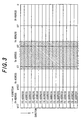
- Fig. 3 is a map view of a display memory having areas of addresses 130 to 17F and capable of accessing 8 bits for each address and displaying data of 5 addresses as a unit.
- the shaded area is a digit data storage area which does not require re-writing of the data for the use of the display memory, that is, it is a write prohibit area.
- the area on the left side of the shaded area is a segment data storage area for the display data output, that is, a write permit area requiring re-writing of data.
- a storage control system will now be described, in which software logic operations are performed for re-writing the data.
- a check is made as to whether an externally supplied address is one in which a write permit area or a write prohibit area is present. If the result of check when the write prohibit area is present in that address is "right", in case when the address contains bits that are not re-written, that is, in order to hold the bit data to be masked, data in which only bits not to be re-written and hence masked are held is obtained by logically ANDing the data in which only write permit data is cleared to "0" among the read-out data and the data having initially been stored in the corresponding address.
- the write data and the data in which write prohibit bits are cleared to "0" are logically ANDed to obtain the data in which only write permit bits are made effective.
- a logical OR operation is executed with the read-out data in which only bits to be masked are held, thus effecting the re-writing of the sole effective bits for the address.
- Fig. 7 shows a flow chart of operation wherein data "01010001B" (B being indicative of binary data) is stored in address No. 165 of the display memory shown in Fig. 3, access address No. 165 and write data "11101000B" is externally supplied.
- address No. 165 0-th bit is a digit data area, i.e., write prohibit area.
- the write data "01010101B” and “11111110B” are logically ANDed, and the write data "01010100B” in which 7-th to 1-st bits are effective data and the read-out data "00000000B” in which only 0-th bit is held are logically ORed.
- the result data "01010100B” is written in address No. 16A of the display memory.
- one re-writing of a segment data group in write permit area i.e., an area of 7-th to 1-st bits of addresses No. 17X and No. 16X in the Fig. 3 example, requires about 220 steps.
- segment data group re-writing requires about 220xn program steps, leading to extreme reduction of the ROM efficiency and program processing efficiency.
- software developers always have to set the mask data in software in advance by taking bits to be masked into considerations.
- Fig. 8 is a block diagram showing a data storage system having a plurality of registers for storing mask data corresponding to the display memory access unit bit width.
- a display memory 10 is accessed in units of 8 bits, and display data is stored in this memory.
- Effective bit width registers 51 to 54 are 8-bit registers, in which mask data corresponding to the access unit (i.e., 8 bits) of the display memory 10 is stored.
- Fig. 9 shows fixed data in the effective bit width registers 51 to 53 when realizing a mask example of data in the display memory 10 shown in Fig. 3.
- Bit “1” is re-writable bit, and bit “0" is bit to be masked.
- a two-dimensional address generator 55 designates an address range of an area in the display memory 10, to which the master data of the effective bit width designation registers 51 to 54 are designated.
- the effective bit width registers 51 to 54 are selected via a selector 56.
- a variable bit width logical operation unit 57 performs operations on externally supplied write data, the mask data from the selected effective bit width register and the data stored in the re-write subject address of the display memory 10 which is as read out by a bit access control unit 58. The result of operations is stored in the re-write subject address of the display memory 10 via the bit access control unit 56.
- the 0-th bit of the external write data is thus nullified, thus providing data "11101000B".
- the variable bit width logic operation unit 57 is supplied with the data "01010001B" in address No. 165 of the display memory 10 via the bit access control unit 58 and executes a logical AND operation of this data "01010001B” and the data "00000001B” as inversion data of the mask data from the effective bit width register 52. The result of operation is "00000001B", and the value of the 0-th bit in the address No. 165 of the display memory 10 is held.
- the external write data having been bit operated is logically ORed with the logically ANDed result of the data "00000001B" as the inversion data of the mask data from the effective bit width register 52 and the data "01010001B” in the address No. 165 of the display memory 10.
- the write mask processed data "11101001B” is written in the address No. 165 of the display memory 10.
- it is required to provide a selector which serves to select registers for setting the mask data in access units of the display memory according to a number of the access unit bit width of the display memory 10 and also select an access unit width register in correspondence to the select address.
- variable bit width logic operation unit 57 performs operations on three different data, i.e., externally supplied write data, the mask data from the selected effective bit width register and the data stored in a re-write subject address of the display memory 10 as read out by the bit access control unit 58. Therefore, the variable bit width logic operation unit is complicated in circuit construction, the number of overall elements is increased, and the chip size is increased. Further, it has been necessary to store the result of operations in the variable bit width logic operation unit 57 in a re-write subject address of the display memory 10 via the bit access control unit 58, thus requiring time for the data write process.
- EP-A-278526 describes a storage control system having a memory and a memory access unit. This system comprises means for holding data to designate an area; means for comparing a memory address and said data; and means for prohibiting writing of data and memory elements corresponding to the area non requiring prewriting of stored contents. By these means it is possible to define a write enable area.
- FIG. 1 is a block diagram showing a first embodiment of the storage control system according to the present invention.
- a display memory 10 has a write permit area and a write prohibit area. Data is written in and read out from the supplied address of the display memory in response to an externally supplied address.
- Fig. 3 shows the memory map of the display memory 10. As shown, the memory has areas of addresses No. 130 to No. 17F. Each address is capable of 8-bit accessing, and data of five addresses can be displayed as one unit data.
- This embodiment is a storage control system 18 comprising a display unit 16 and a microcomputer 17.
- the display unit 16 can display a maximum of 40 bits.
- Display bit width designation data is the output from a CPU 15 of the microcomputer 17 to be input to a display data storage area designation register 11 thereof.
- the display data storage area designation register 11 designates the X direction display bit width of display data stored in the display memory 10.
- Mask bit width designation data is output from the CPU 15 of the microcomputer 17 to be input to a mask bit width designation register 12.
- the mask bit width designation register 12 designates the mask bit width of data to be masked, i.e., data that is not re-written among the display bit widths designated by the display data storage area designation register 11.
- the display data storage area designation register 11 and mask bit width designation register 12 designate X direction bit widths on the map of the display memory 10.
- the CPU 15 outputs address data for designating X and Y direction addresses.
- a write judgment/designation signal generator 13 receives the output of the display data storage area designation register 11, the output of the mask bit width designation register 12 and the address data from the CPU 15 and generates a signal necessary for a write control unit 14.
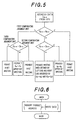
- the operation of the write judgment/designation signal generator will be described with reference to the flow chart of Fig. 5.
- the data of the upper three bits i.e., the 5-th to 3-rd bits
- the data of the lower three bits i.e., the 2-nd to 0-th bits
- the data of the lower three bits i.e., the 2-nd to 0-th bits
- the data as a result of subtraction of data C5 to C3 from the 6-th to 4-th data are denoted by D5 to D3.
- the 6-th to 4-th data which are address data in the X direction of the display memory 10, are denoted by E6 to E4.
- a first comparator compares data E6 to E4 with data B5 to B3. If E6 to E4 ⁇ B5-B3, the pertinent address contains no boundary between a write prohibit area and a write permit area, so that 8-bit data can be re-written.
- a second comparator compares data E6 to E4 with D5 to D3. If E6 to E4 ⁇ D5 to D3, the pertinent address contains the boundary between the write prohibit area and the write permit area, and it is prohibited to write upper bits of the bits designated by data A2 to A0. If the two data compared by the second comparator are the same, the pertinent address contains the right end boundary and left end boundary of the write prohibit area and the write permit area. In this case, the right end boundary is designated by A2 to A0, and the left end boundary by C2 to C0.
- the first comparator compares the data E6 to E4 with the data E5 to E3. If E6 to E4 ⁇ B5 to B3, a third comparator compares the data E6 to E4 with the D5 to D3. If E6 to E4 ⁇ D5 to D3, the pertinent address contains no boundary between the write prohibit area and the write permit area, so that it is prohibited to re-write 8-bit data.
- the pertinent address contains the boundary between the write prohibit area and the write permit area, and it is possible to re-write upper bits of the bits designated by data C2 to C0.
- the third comparator further compares data E6 to E4 with data D5 to D3. If E6 to E4 ⁇ B5 to B3, the pertinent address contains no boundary between the write prohibit area and the write permit area, so that it is possible to re-write 8-bit data.
- four different states of address are defined, i.e., an address in which all the bits are in a write permit area, an address in which upper n bits are in a write permit area and lower (8-n) bits are in a write prohibit area, an address in which all the bits are in a write prohibit area, and an address, in which upper m bits are in a write prohibit area and lower (8-n) bits are in a write permit area.
- the write judgment/designation signal generator 13 determines the address in either of the above four data mask states that corresponds to address data supplied from the CPU 15 and generates a write permit signal and a write prohibit signal with respect to the bit unit corresponding to that address.
- a write control unit 14 writes only effective bits of the write data from the CPU 15 in the display memory 10 according to the write permit signal and write prohibit signal with respect to the bit unit generated from the write judgment/designation signal generator 13.
- an employed bit width of "26 bits” is set in the display data storage area designation register 11, and a mask bit width of "1 bit” is set in the mask bit width designation register 12.
- the used bit width from the address No. 17X side is determined by the data set in the display data storage area designation register 11, that is, the write judgment/designation signal generator 13 determines that the right end of the write prohibit area is the position of the 6-th bit in address No. 14X which is the fourth byte from the address No.
- the write judgment/designation signal generator 13 provides a write permit signal of the 7-th to 1-st bits of the address No. 165 and a write prohibit signal of the 0-bit of that address, and the 7-th to 1-st bits are written as data "1110100XB" (X being indicative of write prohibit) in the display memory 10.
- the write judgment/designation signal generator 13 provides a write permit signal of 7-th to 0-th bits to the write control unit 14, and the data "100010110B" is written in the address No. 170 of the display memory 10.
- the write designation signal generator 13 provides a write prohibit signal of the 7-th 0-th bits to the write control unit 14, so that the data in the address No. 153 is held as such without any writing.
- the display data storage area designation register is constituted by two registers, i.e., an X direction designation register 21a for showing X direction storage area, and a Y direction designation register 21b for showing Y direction storage area.
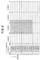
- Fig. 4 shows an example of address map of and display data storage in the display memory 10.
- a display data storage area Enclosed by the broken line rectangle is a display data storage area, and shown shaded is a digit data storage area, i.e., a write prohibit area in which there is no need of re-writing data in the use of the display memory.
- the display memory 10 has areas of addresses No. 130 to No. 17F. Each address is capable of 8-bit accessing, and data of 5 addresses can be displayed as unit data.
- This embodiment is a display memory which is capable of displaying a maximum of 40 bits.
- the X direction in the display data storage area of the display memory 10 are from the 7-bit in address No. 17X to the 6-th bit in address No. 14X, and by setting "12 lines” as lines of use in the Y direction of the Y direction designation register 21b, the Y direction bits in the display data storage area of the display memory 10 are from address No. 1X0 to address No. 1XB.
- the data in these two registers 21a and 21b define a display data storage area as shown enclosed by the broken line rectangle as shown in Fig. 4.
- the X direction data mask area in the display data storage area is from the 11-th bit from the lower side, i.e., the 6-th bit in address 14X to the 0-bit in address No. 16X.
- the display data storage area is up to address 1XB in the Y direction, and this means that the shaded area as shown in Fig. 4 is the write prohibit area in this embodiment.
- the data "01010001B" is stored in address 165 of the display memory 10.
- the write designation signal generator 23 provides a write permit signal of the 7-th to 1-st bits in the address No. 165 to write control unit 14, and the 7-th to 1-st bits are written as data "111010100XB" (X being indicative of write prohibit). Since the 0-th bit is held to be "1B", i.e., data before re-writing, the data in the address No. 165 after re-writing is "11101001B".
- the write judgment/designation signal generator 23 When the CPU 15 provides the write data "01000011B" to address No. 16C, in which all the bits are in a write permit area, the write judgment/designation signal generator 23 provides a write permit signal of 7-th to 0-th bits to the write control unit 14, and the data "01000011B” is written in the address No. 16C of the display memory 10. Likewise, when the CPU 15 provides the write data "10010110B" to address No. 179, in which all the bits are in a write permit area, the write judgment/designation signal generator 23 provides a write permit signal of the 7-th to 0-th bits to the write control unit 14, and data "10010110B" is written in the address No. 179 of the display memory 10.
- the write judgment/designation signal generator 23 provides a write prohibit signal of the 7-th to 0-th bits to the write control unit 14, and the data in the address No. 153 is held without writing of any data.
- the write judgment/designation signal of the 7-th to 0-th is provided to the write control unit 14, data "11010111B" to the address No. 15E of the display memory 10.
- variable bit width logic operation unit 57 performs operations on three different data, i.e., the externally supplied write data, mask data from the selected effective bit width register, and data stored in a re-write subject address of the display memory 10 as read out by the bit access control unit 58. Therefore, the circuit construction of the variable bit width logic operation unit has been complicated, thus leading to increase of the number of the overall elements. However, with the construction of the write judgment/designation signal generator which operates in the manner as shown in Fig. 5, the circuit construction is simplified, so that it is possible to reduce the number of elements.
- the result of operation in the variable bit width logic operation unit 57 is stored in the re-write subject address of the display memory 10 via the bit access control unit 58, thus requiring considerable time in the data re-write process.
- the circuit is simplified, and also the data process is simplified, so that it is possible to reduce time for the data re-writing.
- the Fig. 6 flow of the first and second embodiments of the storage control system can be realized by one step, and thus it is of course possible to increase the process speed.
Landscapes
- Engineering & Computer Science (AREA)
- Theoretical Computer Science (AREA)
- Physics & Mathematics (AREA)
- General Physics & Mathematics (AREA)
- Computer Hardware Design (AREA)
- Radar, Positioning & Navigation (AREA)
- Remote Sensing (AREA)
- General Engineering & Computer Science (AREA)
- Storage Device Security (AREA)
- Controls And Circuits For Display Device (AREA)
- Memory System (AREA)
- Control Of Indicators Other Than Cathode Ray Tubes (AREA)
Claims (3)
- Système de commande de mémorisation pour une mémoire d'affichage (10) ayant un tableau d'éléments de mémoire et une unité d'accès à la mémoire pour accéder à la mémoire d'affichage (10) en unités ayant chacune une largeur d'un nombre prédéterminé de bits, un tel nombre de bits étant supérieur à un, caractérisé en ce que :ledit système de commande de mémorisation comporte :des premiers moyens de maintien (11, 21) pour maintenir des données désignant une zone de mémorisation de données d'affichage de la mémoire d'affichage (10) où des données sont mémorisées,des seconds moyens de maintien (12) pour maintenir des données désignant la largeur d'une zone d'interdiction d'écriture de la mémoire dont le contenu est masqué et non réinscriptible, ces seconds moyens de maintien étant conçus pour désigner ladite largeur en termes de nombre de bits sans tenir compte de si une limite de cette zone d'interdiction d'écriture coïncide avec une frontière d'unité de mémoire ou non,des moyens de comparaison (13, 23) pour comparer une adresse de mémoire délivrée et des données desdits premiers et seconds moyens de maintien, etdes moyens d'interdiction (14) pour interdire l'écriture de données dans un élément de mémoire de la zone d'interdiction d'écriture lorsque le résultat de la comparaison dans les moyens de comparaison (13, 23) indique qu'au moins une partie de la zone d'interdiction d'écriture est contenue dans la largeur binaire de l'unité désignée par l'adresse de mémoire délivrée.
- Système de commande de mémorisation selon la revendication 1, conçu pour écrire des données dans une zone d'autorisation d'écriture, cette zone d'autorisation d'écriture étant la partie de la zone de mémorisation de données d'affichage autre que la zone d'interdiction d'écriture, et pour lire des données à partir de la mémoire d'affichage (10) en réponse à une adresse délivrée depuis l'extérieur, dans lequel :lesdits premiers moyens de maintien (11, 21) comportent un premier registre de désignation de zone de mémorisation de données d'affichage (21a) conçu pour désigner la largeur de données d'affichage mémorisées dans la mémoire d'affichage (10), en réponse à des données de désignation de largeur binaire d'affichage,lesdits seconds moyens de maintien (12) comportent un registre de désignation de largeur binaire de masque conçu pour désigner la largeur des données à masquer, c'est-à-dire des données qui ne sont pas réécrites dans la largeur des données d'affichage désignées par le premier registre de désignation de zone de mémorisation de données d'affichage, en réponse à des données de désignation de largeur binaire de masque,ledit premier registre de désignation de zone de mémorisation de données d'affichage et ledit registre de désignation de largeur binaire de masque (12) désignant des largeurs dans la direction X en termes de nombre de bits sur la carte de la mémoire d'affichage (10),lesdits moyens de comparaison (13, 23) comportent un générateur de signal de détermination/désignation d'écriture (13, 23) pour déterminer les extrémités opposées de la zone d'interdiction d'écriture dans la mémoire d'affichage pour définir quatre états d'adresse différents, un état d'adresse dans lequel tous les bits sont dans la zone d'autorisation d'écriture, un état d'adresse dans lequel des bits supérieurs prédéterminés sont dans la zone d'autorisation d'écriture et des bits inférieurs prédéterminés dans la zone d'interdiction d'écriture, un état d'adresse dans lequel tous les bits sont dans la zone d'interdiction d'écriture, et un état d'adresse dans lequel des bits supérieurs prédéterminés sont dans la zone d'interdiction d'écriture et des bits inférieurs prédéterminés sont dans la zone d'autorisation d'écriture, déterminer l'état d'adresse dans l'un des quatre états d'adresse qui correspond à des données d'adresse délivrées, et générer un signal d'autorisation d'écriture et un signal d'interdiction d'écriture se rapportant à une unité binaire correspondant aux données d'adresse délivrées, etlesdits moyens d'interdiction (14) comportent une unité de commande d'écriture pour écrire uniquement des bits autorisés des données d'écriture dans la mémoire d'affichage (10) conformément au signal d'autorisation d'écriture et au signal d'interdiction d'écriture délivrés par le générateur de signal de détermination/désignation d'écriture se rapportant à l'unité binaire correspondant aux données d'adresse délivrées.
- Système de commande de mémorisation selon la revendication 2, dans lequel :lesdits premiers moyens de maintien (21) comportent un second registre de désignation de zone de mémorisation de données d'affichage (21 b) pour désigner la largeur dans la direction Y de données d'affichage mémorisées dans la mémoire d'affichage (10), en réponse à des données de désignation de largeur binaire d'affichage.
Applications Claiming Priority (3)
| Application Number | Priority Date | Filing Date | Title |
|---|---|---|---|
| JP6253852A JP2729151B2 (ja) | 1994-10-19 | 1994-10-19 | 記憶制御装置 |
| JP253852/94 | 1994-10-19 | ||
| JP25385294 | 1994-10-19 |
Publications (2)
| Publication Number | Publication Date |
|---|---|
| EP0708429A1 EP0708429A1 (fr) | 1996-04-24 |
| EP0708429B1 true EP0708429B1 (fr) | 2004-09-15 |
Family
ID=17257037
Family Applications (1)
| Application Number | Title | Priority Date | Filing Date |
|---|---|---|---|
| EP95116374A Expired - Lifetime EP0708429B1 (fr) | 1994-10-19 | 1995-10-17 | Système de commande de mémoire pour interdire la réecriture dans une région prédéterminée de la mémoire |
Country Status (6)
| Country | Link |
|---|---|
| US (1) | US5777632A (fr) |
| EP (1) | EP0708429B1 (fr) |
| JP (1) | JP2729151B2 (fr) |
| KR (1) | KR100225726B1 (fr) |
| CN (1) | CN1084895C (fr) |
| DE (1) | DE69533499D1 (fr) |
Families Citing this family (3)
| Publication number | Priority date | Publication date | Assignee | Title |
|---|---|---|---|---|
| USRE38997E1 (en) * | 1995-02-03 | 2006-02-28 | Kabushiki Kaisha Toshiba | Information storage and information processing system utilizing state-designating member provided on supporting card surface which produces write-permitting or write-inhibiting signal |
| JP3660382B2 (ja) * | 1995-02-03 | 2005-06-15 | 株式会社東芝 | 情報記憶装置およびそれに用いるコネクタ部 |
| JP6396373B2 (ja) * | 2016-07-26 | 2018-09-26 | ファナック株式会社 | フィルタ回路、フィルタ回路を備えた通信回路及びフィルタ回路を備えた数値制御装置 |
Family Cites Families (17)
| Publication number | Priority date | Publication date | Assignee | Title |
|---|---|---|---|---|
| JPS60147785A (ja) * | 1984-01-12 | 1985-08-03 | 株式会社アスキ− | 論理領域間デ−タ移動制御装置 |
| US4710767A (en) * | 1985-07-19 | 1987-12-01 | Sanders Associates, Inc. | Method and apparatus for displaying multiple images in overlapping windows |
| US5185859A (en) * | 1985-10-22 | 1993-02-09 | Texas Instruments Incorporated | Graphics processor, a graphics computer system, and a process of masking selected bits |
| JPS62157460A (ja) * | 1985-12-28 | 1987-07-13 | Toshiba Corp | 画像デ−タ書込み制御装置 |
| US4941111A (en) * | 1986-04-18 | 1990-07-10 | Advanced Micro Devices, Inc. | Video picking and clipping method and apparatus |
| JPS638951A (ja) | 1986-06-30 | 1988-01-14 | Toshiba Corp | 情報記憶装置 |
| JPS6367867A (ja) * | 1986-09-10 | 1988-03-26 | Fuji Xerox Co Ltd | 画像処理方法 |
| JP2541539B2 (ja) * | 1987-02-13 | 1996-10-09 | 日本電気株式会社 | 図形処理装置 |
| JPH01233590A (ja) * | 1988-03-14 | 1989-09-19 | Toshiba Corp | 携帯可能電子装置 |
| US5274364A (en) * | 1989-01-09 | 1993-12-28 | Industrial Technology Research Institute | Window clipping method and device |
| JPH0322058A (ja) * | 1989-06-20 | 1991-01-30 | Oki Electric Ind Co Ltd | アドレス検証方法 |
| US5255360A (en) * | 1990-09-14 | 1993-10-19 | Hughes Aircraft Company | Dual programmable block texturing and complex clipping in a graphics rendering processor |
| US5218674A (en) * | 1990-09-14 | 1993-06-08 | Hughes Aircraft Company | Hardware bit block transfer operator in a graphics rendering processor |
| JP3016490B2 (ja) * | 1990-09-28 | 2000-03-06 | 富士写真フイルム株式会社 | Icメモリカード |
| US5276437A (en) * | 1992-04-22 | 1994-01-04 | International Business Machines Corporation | Multi-media window manager |
| JP3413201B2 (ja) * | 1992-12-17 | 2003-06-03 | セイコーエプソン株式会社 | ウィンドウ型及び他の表示オペレーションのためのグラフィックス制御プレーン |
| US5493646A (en) * | 1994-03-08 | 1996-02-20 | Texas Instruments Incorporated | Pixel block transfer with transparency |
-
1994
- 1994-10-19 JP JP6253852A patent/JP2729151B2/ja not_active Expired - Lifetime
-
1995
- 1995-10-17 EP EP95116374A patent/EP0708429B1/fr not_active Expired - Lifetime
- 1995-10-17 DE DE69533499T patent/DE69533499D1/de not_active Expired - Fee Related
- 1995-10-19 US US08/545,405 patent/US5777632A/en not_active Expired - Lifetime
- 1995-10-19 CN CN95119937A patent/CN1084895C/zh not_active Expired - Fee Related
- 1995-10-19 KR KR1019950036814A patent/KR100225726B1/ko not_active IP Right Cessation
Also Published As
| Publication number | Publication date |
|---|---|
| US5777632A (en) | 1998-07-07 |
| CN1151048A (zh) | 1997-06-04 |
| KR960015208A (ko) | 1996-05-22 |
| KR100225726B1 (ko) | 1999-10-15 |
| EP0708429A1 (fr) | 1996-04-24 |
| DE69533499D1 (de) | 2004-10-21 |
| CN1084895C (zh) | 2002-05-15 |
| JPH08115256A (ja) | 1996-05-07 |
| JP2729151B2 (ja) | 1998-03-18 |
Similar Documents
| Publication | Publication Date | Title |
|---|---|---|
| US4710767A (en) | Method and apparatus for displaying multiple images in overlapping windows | |
| US5530938A (en) | Non-volatile memory card device having flash EEPROM memory chips with designated spare memory chips and the method of rewriting data into the memory card device | |
| US4736200A (en) | Graphic processing apparatus with clipping circuit | |
| US5093783A (en) | Microcomputer register bank accessing | |
| EP0845786A2 (fr) | Microordinateur comprenant EEPROM flash | |
| KR910000365B1 (ko) | 기억회로 | |
| EP0280320B1 (fr) | Commande d'affichage graphique équipée d'un circuit de recherche de bordure | |
| EP0708429B1 (fr) | Système de commande de mémoire pour interdire la réecriture dans une région prédéterminée de la mémoire | |
| US4672538A (en) | Method of dynamically changing formation of addresses in memory of a data processing system | |
| EP0147542B1 (fr) | Système d'affichage à fenêtres multiples | |
| US4868553A (en) | Raster operation device | |
| JPS592079A (ja) | 画像記憶装置 | |
| JPH0452476B2 (fr) | ||
| JPH11259357A (ja) | 半導体集積装置及び不揮発性メモリ書き込み方式 | |
| US5619714A (en) | Microcomputer having an instruction decoder with a fixed area and a rewritable area | |
| KR960002974B1 (ko) | Z버퍼 메모리를 사용한 윈도우(window)확장장치 | |
| KR940014242A (ko) | 퍼지 추론 전용 명령을 내장하는 마이크로컴퓨터 | |
| JP2886855B2 (ja) | 画像表示装置 | |
| JPS58111171A (ja) | メモリアクセス方式 | |
| JPS6148174B2 (fr) | ||
| JP2635426B2 (ja) | 背景色表示処理装置 | |
| KR830000265B1 (ko) | 정보처리 장치 | |
| JPH0528771A (ja) | メモリ素子 | |
| JPH07320045A (ja) | 画像処理装置 | |
| JPH05225044A (ja) | メモリ集積回路 |
Legal Events
| Date | Code | Title | Description |
|---|---|---|---|
| PUAI | Public reference made under article 153(3) epc to a published international application that has entered the european phase |
Free format text: ORIGINAL CODE: 0009012 |
|
| 17P | Request for examination filed |
Effective date: 19960229 |
|
| AK | Designated contracting states |
Kind code of ref document: A1 Designated state(s): DE FR GB |
|
| 17Q | First examination report despatched |
Effective date: 19990318 |
|
| RAP1 | Party data changed (applicant data changed or rights of an application transferred) |
Owner name: NEC ELECTRONICS CORPORATION Owner name: NEC CORPORATION |
|
| GRAP | Despatch of communication of intention to grant a patent |
Free format text: ORIGINAL CODE: EPIDOSNIGR1 |
|
| GRAS | Grant fee paid |
Free format text: ORIGINAL CODE: EPIDOSNIGR3 |
|
| GRAA | (expected) grant |
Free format text: ORIGINAL CODE: 0009210 |
|
| AK | Designated contracting states |
Kind code of ref document: B1 Designated state(s): DE FR GB |
|
| PG25 | Lapsed in a contracting state [announced via postgrant information from national office to epo] |
Ref country code: FR Free format text: LAPSE BECAUSE OF FAILURE TO SUBMIT A TRANSLATION OF THE DESCRIPTION OR TO PAY THE FEE WITHIN THE PRESCRIBED TIME-LIMIT Effective date: 20040915 |
|
| REG | Reference to a national code |
Ref country code: GB Ref legal event code: FG4D |
|
| PGFP | Annual fee paid to national office [announced via postgrant information from national office to epo] |
Ref country code: GB Payment date: 20041013 Year of fee payment: 10 |
|
| REF | Corresponds to: |
Ref document number: 69533499 Country of ref document: DE Date of ref document: 20041021 Kind code of ref document: P |
|
| PG25 | Lapsed in a contracting state [announced via postgrant information from national office to epo] |
Ref country code: DE Free format text: LAPSE BECAUSE OF NON-PAYMENT OF DUE FEES Effective date: 20050503 |
|
| PLBE | No opposition filed within time limit |
Free format text: ORIGINAL CODE: 0009261 |
|
| STAA | Information on the status of an ep patent application or granted ep patent |
Free format text: STATUS: NO OPPOSITION FILED WITHIN TIME LIMIT |
|
| 26N | No opposition filed |
Effective date: 20050616 |
|
| EN | Fr: translation not filed | ||
| PG25 | Lapsed in a contracting state [announced via postgrant information from national office to epo] |
Ref country code: GB Free format text: LAPSE BECAUSE OF NON-PAYMENT OF DUE FEES Effective date: 20051017 |
|
| GBPC | Gb: european patent ceased through non-payment of renewal fee |
Effective date: 20051017 |