EP0704877A1 - Elektrischer Schutz von einer Anode eines flachen Bildschirms - Google Patents
Elektrischer Schutz von einer Anode eines flachen Bildschirms Download PDFInfo
- Publication number
- EP0704877A1 EP0704877A1 EP95410112A EP95410112A EP0704877A1 EP 0704877 A1 EP0704877 A1 EP 0704877A1 EP 95410112 A EP95410112 A EP 95410112A EP 95410112 A EP95410112 A EP 95410112A EP 0704877 A1 EP0704877 A1 EP 0704877A1
- Authority
- EP
- European Patent Office
- Prior art keywords
- interconnection
- anode
- strips
- screen
- track
- Prior art date
- Legal status (The legal status is an assumption and is not a legal conclusion. Google has not performed a legal analysis and makes no representation as to the accuracy of the status listed.)
- Granted
Links
- OAICVXFJPJFONN-UHFFFAOYSA-N Phosphorus Chemical compound [P] OAICVXFJPJFONN-UHFFFAOYSA-N 0.000 claims description 31
- 239000004020 conductor Substances 0.000 claims description 21
- 238000009413 insulation Methods 0.000 claims description 15
- 238000007650 screen-printing Methods 0.000 claims description 5
- 238000002955 isolation Methods 0.000 abstract 1
- 239000007787 solid Substances 0.000 abstract 1
- 230000001066 destructive effect Effects 0.000 description 5
- 230000015572 biosynthetic process Effects 0.000 description 4
- 238000005516 engineering process Methods 0.000 description 4
- 238000000034 method Methods 0.000 description 4
- 230000010287 polarization Effects 0.000 description 4
- 239000000758 substrate Substances 0.000 description 4
- VAYOSLLFUXYJDT-RDTXWAMCSA-N Lysergic acid diethylamide Chemical compound C1=CC(C=2[C@H](N(C)C[C@@H](C=2)C(=O)N(CC)CC)C2)=C3C2=CNC3=C1 VAYOSLLFUXYJDT-RDTXWAMCSA-N 0.000 description 3
- 239000000470 constituent Substances 0.000 description 3
- 238000010586 diagram Methods 0.000 description 3
- 239000003086 colorant Substances 0.000 description 2
- 238000000151 deposition Methods 0.000 description 2
- 239000011521 glass Substances 0.000 description 2
- AMGQUBHHOARCQH-UHFFFAOYSA-N indium;oxotin Chemical compound [In].[Sn]=O AMGQUBHHOARCQH-UHFFFAOYSA-N 0.000 description 2
- 238000004519 manufacturing process Methods 0.000 description 2
- 229910018487 Ni—Cr Inorganic materials 0.000 description 1
- 230000008859 change Effects 0.000 description 1
- VNNRSPGTAMTISX-UHFFFAOYSA-N chromium nickel Chemical compound [Cr].[Ni] VNNRSPGTAMTISX-UHFFFAOYSA-N 0.000 description 1
- 230000008021 deposition Effects 0.000 description 1
- 230000005684 electric field Effects 0.000 description 1
- 239000010408 film Substances 0.000 description 1
- 239000012212 insulator Substances 0.000 description 1
- 230000004048 modification Effects 0.000 description 1
- 238000012986 modification Methods 0.000 description 1
- 230000008520 organization Effects 0.000 description 1
- 230000009467 reduction Effects 0.000 description 1
- 229910052710 silicon Inorganic materials 0.000 description 1
- 239000010703 silicon Substances 0.000 description 1
- 125000006850 spacer group Chemical group 0.000 description 1
- 239000010409 thin film Substances 0.000 description 1
Images


Classifications
-
- H—ELECTRICITY
- H01—ELECTRIC ELEMENTS
- H01J—ELECTRIC DISCHARGE TUBES OR DISCHARGE LAMPS
- H01J17/00—Gas-filled discharge tubes with solid cathode
- H01J17/02—Details
- H01J17/04—Electrodes; Screens
- H01J17/12—Control electrodes
-
- H—ELECTRICITY
- H01—ELECTRIC ELEMENTS
- H01J—ELECTRIC DISCHARGE TUBES OR DISCHARGE LAMPS
- H01J29/00—Details of cathode-ray tubes or of electron-beam tubes of the types covered by group H01J31/00
- H01J29/02—Electrodes; Screens; Mounting, supporting, spacing or insulating thereof
- H01J29/10—Screens on or from which an image or pattern is formed, picked up, converted or stored
-
- G—PHYSICS
- G09—EDUCATION; CRYPTOGRAPHY; DISPLAY; ADVERTISING; SEALS
- G09G—ARRANGEMENTS OR CIRCUITS FOR CONTROL OF INDICATING DEVICES USING STATIC MEANS TO PRESENT VARIABLE INFORMATION
- G09G3/00—Control arrangements or circuits, of interest only in connection with visual indicators other than cathode-ray tubes
- G09G3/20—Control arrangements or circuits, of interest only in connection with visual indicators other than cathode-ray tubes for presentation of an assembly of a number of characters, e.g. a page, by composing the assembly by combination of individual elements arranged in a matrix no fixed position being assigned to or needed to be assigned to the individual characters or partial characters
- G09G3/22—Control arrangements or circuits, of interest only in connection with visual indicators other than cathode-ray tubes for presentation of an assembly of a number of characters, e.g. a page, by composing the assembly by combination of individual elements arranged in a matrix no fixed position being assigned to or needed to be assigned to the individual characters or partial characters using controlled light sources
-
- H—ELECTRICITY
- H01—ELECTRIC ELEMENTS
- H01J—ELECTRIC DISCHARGE TUBES OR DISCHARGE LAMPS
- H01J29/00—Details of cathode-ray tubes or of electron-beam tubes of the types covered by group H01J31/00
- H01J29/96—One or more circuit elements structurally associated with the tube
-
- H—ELECTRICITY
- H01—ELECTRIC ELEMENTS
- H01J—ELECTRIC DISCHARGE TUBES OR DISCHARGE LAMPS
- H01J31/00—Cathode ray tubes; Electron beam tubes
- H01J31/08—Cathode ray tubes; Electron beam tubes having a screen on or from which an image or pattern is formed, picked up, converted, or stored
- H01J31/10—Image or pattern display tubes, i.e. having electrical input and optical output; Flying-spot tubes for scanning purposes
- H01J31/12—Image or pattern display tubes, i.e. having electrical input and optical output; Flying-spot tubes for scanning purposes with luminescent screen
- H01J31/123—Flat display tubes
Definitions
- the present invention relates to a flat display screen anode. It applies more particularly to the production of connections of luminescent elements of an anode of a color screen, such as a microtip color screen.
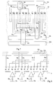
- FIG. 1 represents the structure of a flat screen with microtips of the type to which the invention relates.
- Such a microtip screen essentially consists of a cathode 1 with microtips 2 and a grid 3 provided with holes 4 corresponding to the locations of the microtips 2.
- the cathode 1 is placed opposite a cathodoluminescent anode 5 including a substrate of glass 6 constitutes the screen surface.
- the cathode 1 is organized in columns and consists, on a glass substrate 10, of cathode conductors organized in meshes from a conductive layer.
- the microtips 2 are produced on a resistive layer 11 deposited on the cathode conductors and are arranged inside the meshes defined by the conductors of cathode.
- FIG. 1 partially represents the interior of a mesh, the cathode conductors do not appear in this figure.
- the cathode 1 is associated with the grid 3 which is organized in lines. The intersection of a line of the grid 3 and a column of the cathode 1 defines a pixel.
- This device uses the electric field created between the cathode 1 and the grid 3 so that electrons are extracted from the microtips 2 towards phosphor elements 7 of the anode 5.
- the anode 5 is provided alternating bands of phosphor elements 7r, 7b, 7g each corresponding to a color (Blue, Red, Green). The strips are separated from each other by an insulator 8.
- the phosphor elements 7 are deposited on electrodes 9, consisting of corresponding strips of a transparent conductive layer such as indium tin oxide (ITO) .
- ITO indium tin oxide
- the sets of blue, red and green bands are alternately polarized with respect to the cathode 1, so that the electrons extracted from the microtips 2 of a pixel of the cathode / grid are alternately directed towards the phosphor elements 7 opposite each other colours.
- the command to select the phosphor 7 (the phosphor 7g in FIG. 1) which must be bombarded by the electrons coming from the microtips 2 of the cathode 1 requires selectively controlling the polarization of the phosphor elements 7 of the anode 5, color by color .
- FIG. 2 schematically illustrates a conventional color screen anode structure. This figure partially shows, in elevation on the phosphor side, an anode 5 produced according to known techniques.
- the strips 9 of anode electrodes, deposited on the substrate 6, are interconnected outside the useful surface of the screen, by color of phosphor elements 7 to be connected to a control system (not shown).
- Two interconnection tracks 12 and 13, respectively anode electrodes 9g and 9b, are produced for two of the three colors of phosphor elements (for example 7g and 7b).
- An insulation layer 14 (shown in dashed lines in FIG. 2) is deposited on the interconnection track 13.
- a third interconnection track 15 is connected, by means of conductors 16 deposited on the insulation layer 14, to the anode electrode strips 9r intended for the phosphor elements 7r of the third color.
- the rows of the grid 3 are sequentially polarized at a potential of the order of 80 V while the strips of phosphor elements (for example 7g in FIG. 1) to be excited are polarized under a voltage of the order of 400V, the other bands (for example 7r and 7b in FIG. 1) being at zero potential.
- the columns of cathode 1, the potential of which represents for each row of grid 5 the brightness of the pixel defined by the intersection of the column of cathode and of the row of grid 5 in the color considered, are brought to respective potentials between a maximum emission potential and a non-emission potential (for example 0 and 30 V respectively).
- the potential difference between the anode and the cathode is related to the inter-electrode distance.
- a maximum potential difference is sought for reasons of screen brightness, which means that an inter-electrode distance which is as large as possible is sought.
- the structure of the inter-electrode space which includes spacers capable of creating shadow areas in the screen if they are too large, prevents this inter-electrode distance from being increased.
- the inter-electrode space of a conventional screen is therefore of the order of 0.2 mm. This leads to choosing an anode-cathode voltage value which is critical from the point of view of the formation of electric arcs.
- Destructive electric arcs can then occur at the slightest dimensional irregularity in the distance between a microtip or the grid layer and the phosphor elements of the anode. In addition, such irregularities are inevitable, given the small dimensions and the techniques employed for producing the anode and the grid cathode.
- the resistive layer 11 makes it possible to limit the formation of destructive short circuits between the microtips and the grid.
- arcs can occur between the grid 3 and those of the phosphor elements 7 of the anode which are polarized to attract the electrons emitted by the microtips 2 (for example the phosphors 7g in FIG. 1). Arcs can also occur between two neighboring bands of phosphor elements (for example 7g and 7r in FIG. 1) due to the difference in potential between these two bands.
- the invention aims to overcome these drawbacks by proposing a flat screen microdot display anode which eliminates the risk of the appearance of electric arcs between the anode and the grid or between two neighboring strips of phosphor elements of the anode, without affecting the brightness of the screen.
- the present invention provides a flat display screen anode, of the type comprising at least one set of strips of phosphor elements deposited on corresponding conductive strips and at least one interconnection conductor of the strips of said set.
- the conductive strips of said assembly are interconnected by means of resistors placed in series between the conductive strips and said interconnection conductor with which they are associated.
- each conductive strip is individually connected to the interconnection conductor via a resistor.
- the same resistance is associated with several conductive strips of the assembly.
- the resistors are produced by screen printing in thick layer of resistive sections on an insulation layer deposited at least on a track constituting the interconnection conductor, the insulation layer being open locally to the vertical alignment of the ends of each resistive section to allow the electrical connection of these ends, respectively to one end of at least one conductive strip and to the interconnection track.
- the insulation layer extends over the entire surface of the anode and is open, in the useful surface of the screen, directly above each conductive strip.
- all the resistive sections associated with the interconnection track are of the same length.
- the anode comprises three sets of alternating bands of phosphor elements each corresponding to a color and at least three interconnection conductors of the bands of the same color.
- all the resistive sections associated with the same interconnection track are of the same length and extend from one end of a conductive strip to the interconnection track at which this strip is associated.
- all the interconnection tracks are deposited in a same side of the anode being parallel to each other and perpendicular to the conductive strips.
- At least two interconnection tracks perpendicular to the conductive strips surround these conductive strips.
- An essential characteristic of the present invention is to propose the realization of the interconnections of the anode conductor strips polarizing the phosphor elements, by means of resistors placed in series. between the conductive strips and the interconnection track with which they are associated.
- the present invention provides for polarizing each band of phosphor elements, or a small group of bands of phosphor elements of the same color, by means of a resistor placed in series between this band, or this small group, and the interconnection track with which it is associated.
- Resistors of sufficiently large values can therefore be provided to create in the characteristics "anode current - cathode voltage" and "anode current - voltage between two adjacent anode conductive strips", a load line making it possible to limit the appearance of electric arcs.
- the value of the resistors is preferably chosen so as not to cause a decrease in the anode voltage of more than a few percent so as not to cause a change in the brightness of the screen which is perceptible. for the user and also so as not to cause a noticeable stray power dissipation.
- These resistances can also be produced using thin film technology by depositing these layers above or below the conductive strips. These layers may, for example, be made of doped silicon, amorphous or polycrystalline, or nickel-chromium.
- resistors according to the technology of thick layers, for example by means of a deposition by screen printing of a resistive ink or paste of the type of those used in hybrid circuits.
- the invention proposes to electrically isolate all the conductive strips of the anode not only between them but also interconnection tracks, then to affix a resistive layer between each conductive strip, or group of a few strips, and the interconnection track.
- an anode according to a first embodiment of the invention consists of parallel conductive strips 9r, 9g, 9b deposited on a substrate 6 and intended to receive in the useful surface of the screen of the phosphor elements (not shown).
- these bands must be able to be polarized sequentially by sets of bands of the same color (red, green, blue).
- Each strip 9r, 9b, 9g is individually connected to an interconnection track 21r, 21g, 21b respectively of the strips of the same color, via a resistive section 22.
- the resistive sections (for example 22r) associated to an interconnection track (for example 21r) are electrically isolated from the two other interconnection tracks (for example 21g, 21b).
- an insulation layer 23 is interposed at least on the two interconnection tracks 21g and 21b which are closest to the ends of the conductive strips 9.
- the insulating layer 23 covers the entire anode and is partially open directly above the two ends of each resistive section 22 to allow the electrical connection of these ends, respectively at one end d 'a conductive strip 9 and to an interconnection track 21. If the insulation layer 23 covers the entire anode, it is also conventionally open, in the useful surface of the screen directly above each conductive strip 9 to receive the phosphor elements. In other words, the insulation layer 23 is in this case merged with the insulation layer 8 (FIG. 1) of the phosphor elements between them.
- Openings 24r, 24g, 24b and 25r, 25g, 25b are made in the insulation layer 23 directly above the ends of the resistive sections 22r, 22g, 22b, respectively opposite an interconnection track 21r, 21g , 21b and the end of a conductive strip 9r, 9g, 9b.
- each interconnection track 21 and a strip 9 of phosphor elements is effected by means of a series resistor constituted by a resistive section 22.
- the resistive sections 22 are dimensioned to all have the same resistance value between their ends, at least for all the sections associated with the same interconnection track, therefore to the same color.
- all the resistive sections associated with the same interconnection track have the same length and the same section which fix the value of the series resistance between a conductive strip and the interconnection track with which it is associated.
- all the resistive sections 22 of the screen have the same section and the same length.
- FIG. 5 represents the equivalent electrical diagram of the embodiment represented in FIG. 3.
- Each conductive strip 9 is individually protected against electric arcs by a series resistance Ra of high value between this strip and the interconnection track 21 with which it is associated.
- the resistance Ra is chosen from a value such that it limits the current in the conductive strip 9 to a given value chosen to avoid the appearance of destructive electric arcs, without however causing a significant drop in the anode voltage. .
- the microdots of the cathode 1 have been represented in the form of a microdots 2 per pixel whereas they are in reality several thousand per screen pixel.
- a resistance Rk thus appears which corresponds to the resistive layer 11 between the cathode conductors and the microtips. This resistance Rk makes it possible to homogenize the electronic emission of the microtips 2 and to avoid the appearance of short circuits between the grid 3 and the microtips.
- the resistance Ra provided by a given resistive section is electrically in series with this resistance Rk globalized at the level of a pixel.
- the value of the resistance Rk globalized at the level of a pixel is of the order of 2 M ⁇ and is found in series with the value of the resistance Ra which is of the same order of magnitude (about 0.7 M ⁇ ).
- the addition of such resistive sections does not harm the electronic emission of the microtips of a given pixel.
- a resistor of the order of 670 k ⁇ limits the voltage drop across the resistor to around 2%.
- Such a resistance value makes it possible to prevent the formation of destructive electric arcs by limiting the current in the conductive strip to 0.7 mA, while making the reduction in brightness of the screen imperceptible.
- the addition of these resistances Ra does not harm the switching speed of the anode lines. Indeed, although the value of the resistance Ra intervenes on the time constant of the RC cell constituted by the association of this resistance with the capacity and the intrinsic resistance of the conductive strip, the value of the time constant obtained remains perfectly acceptable. For example, for the pixel furthest from the interconnection track, the capacity of an ITO anode conductive strip (transparent conductor based on indium tin oxide) is l '' order of 30 pF for 30 cm long and its intrinsic resistance is of the order of 20 k ⁇ . The time constant introduced by the addition of a resistance Ra is 20 ⁇ s, which is perfectly acceptable. In fact, each anode strip remaining polarized during the whole time of the grid line scanning, the switching of the anode lines conventionally occurs for a color screen only 3 to 6 times per image depending on the organization of the addressing.
- Resistances Ra with a value of approximately 670 k ⁇ can be produced using the thick film technology with an ink having a resistivity of 50 k ⁇ / square, by means of resistive sections 22 with a width of approximately 75 ⁇ m, d '' a thickness of about 10 ⁇ m and a length of 1 mm.
- FIG. 6 illustrates a variant of the embodiment shown in FIG. 3.
- the interconnection tracks are not all placed on the same side of the anode.
- two tracks for example 21r and 21g
- the third track for example 21b
- Such an alternative embodiment makes it possible to require less precision for the screen printing of the resistive sections 22 in thick layers.
- FIGS. 7 and 8 illustrate another embodiment of the present invention which also makes it possible to facilitate the production of the resistive sections according to the technology of thick layers.
- the conductive strips 9 of the anode are no longer individually connected to an interconnection track, but by group of a small number of strips of the same color.
- the conductive strips of the same color are connected three by three to an interconnection track, by means of a resistive section 22.
- the conductive strips 9r are connected in groups of three consecutive strips, by their ends located on the side of the track 21r, by means of tracks 26r parallel to the interconnection tracks.
- the conductive strips 9g are connected in groups of three consecutive strips, by their ends located on the side of the track 21g, also at the using 26g tracks parallel to the interconnection tracks.
- the conductive strips 9b of the third color they are connected three by three, but directly by means of the resistive sections 22b.
- an insulation layer 23 is preferably deposited over the entire surface of the anode. This layer is open, in line with the strips 9 in the useful surface of the screen for receiving the phosphor elements, and outside the useful surface of the screen to make the interconnections via the resistive sections 22. Openings 25r, 25g and 25b are formed in the insulation layer 23 directly above one of the ends of the resistive sections 22r, 22g and 22b, respectively opposite the interconnection tracks 21r, 21g and 21b. Openings 24r and 24g are made plumb with the other end of the resistive sections 22r and 22g, respectively at the level of tracks 26r and 26g. Openings 24b are made directly above the end of each conductive strip 9b which is on the side of the interconnection track 21b.
- each strip 9b of the third color has at its end located on the side of the track 21b, a stud 27 plumb with which an opening 24b is made. This is to allow the strips 9b to be easily connected, three by three, via the same resistive section 22b, to the interconnection track 21b.
- each group of three bands of the same color is connected individually by means of a resistance Ra, to an interconnection track of the bands of the same color.
- the choice of embodiment depends for example on the width of the anode conductive strips, therefore on the size screen pixels. In fact, the more the size of the pixels is reduced, the narrower the conductive strips 9 and the more the accuracy of the screen printing of the resistive sections in thick layers will be critical.
- the embodiment of FIG. 3 will be chosen with resistive sections 22 of 75 ⁇ m wide, the pitch between the strips of anode conductors being 100 ⁇ m.
- each of the constituents described for the constituent layers of the anode may be replaced by one or more constituents fulfilling the same function.
Landscapes
- Engineering & Computer Science (AREA)
- Physics & Mathematics (AREA)
- Computer Hardware Design (AREA)
- General Physics & Mathematics (AREA)
- Theoretical Computer Science (AREA)
- Cathode-Ray Tubes And Fluorescent Screens For Display (AREA)
- Video Image Reproduction Devices For Color Tv Systems (AREA)
Applications Claiming Priority (2)
| Application Number | Priority Date | Filing Date | Title |
|---|---|---|---|
| FR9411806 | 1994-09-28 | ||
| FR9411806A FR2725072A1 (fr) | 1994-09-28 | 1994-09-28 | Protection electrique d'une anode d'ecran plat de visualisation |
Publications (2)
| Publication Number | Publication Date |
|---|---|
| EP0704877A1 true EP0704877A1 (de) | 1996-04-03 |
| EP0704877B1 EP0704877B1 (de) | 1999-01-07 |
Family
ID=9467520
Family Applications (1)
| Application Number | Title | Priority Date | Filing Date |
|---|---|---|---|
| EP95410112A Expired - Lifetime EP0704877B1 (de) | 1994-09-28 | 1995-09-25 | Elektrischer Schutz von einer Anode eines flachen Bildschirms |
Country Status (7)
| Country | Link |
|---|---|
| US (1) | US5592056A (de) |
| EP (1) | EP0704877B1 (de) |
| JP (1) | JPH08236047A (de) |
| KR (1) | KR960012156A (de) |
| CN (1) | CN1129848A (de) |
| DE (1) | DE69507101T2 (de) |
| FR (1) | FR2725072A1 (de) |
Cited By (2)
| Publication number | Priority date | Publication date | Assignee | Title |
|---|---|---|---|---|
| EP1073088A1 (de) * | 1999-07-27 | 2001-01-31 | Commissariat à l'Energie Atomique | Herstellung einer Anode eines flachen Bildschirms, nach diesem Verfahren hergestellte Anode und Verwendung dieser Anode für einen flachen Schirm |
| EP1638129A3 (de) * | 2004-09-21 | 2007-11-07 | Canon Kabushiki Kaisha | Strahlungsemittierender Bildschirm und Bilderzeugungsgerät |
Families Citing this family (23)
| Publication number | Priority date | Publication date | Assignee | Title |
|---|---|---|---|---|
| FR2723254B1 (fr) * | 1994-07-26 | 1996-10-11 | Pixel Int Sa | Anode d'ecran plat de visualisation |
| FR2732160B1 (fr) * | 1995-03-22 | 1997-06-13 | Pixtech Sa | Anode d'ecran plat de visualisation a bandes resistives |
| US5952987A (en) * | 1996-01-18 | 1999-09-14 | Micron Technology, Inc. | Method and apparatus for improved gray scale control in field emission displays |
| JP3199682B2 (ja) | 1997-03-21 | 2001-08-20 | キヤノン株式会社 | 電子放出装置及びそれを用いた画像形成装置 |
| US6013986A (en) * | 1997-06-30 | 2000-01-11 | Candescent Technologies Corporation | Electron-emitting device having multi-layer resistor |
| US6323831B1 (en) * | 1997-09-17 | 2001-11-27 | Kabushiki Kaisha Toshiba | Electron emitting device and switching circuit using the same |
| FR2769114B1 (fr) * | 1997-09-30 | 1999-12-17 | Pixtech Sa | Simplification de l'adressage d'un ecran a micropointes |
| US6144144A (en) * | 1997-10-31 | 2000-11-07 | Candescent Technologies Corporation | Patterned resistor suitable for electron-emitting device |
| JP2000311642A (ja) | 1999-02-22 | 2000-11-07 | Canon Inc | 画像形成装置 |
| US6771236B1 (en) * | 1999-03-05 | 2004-08-03 | Sony Corporation | Display panel and display device to which the display panel is applied |
| JP2003178690A (ja) * | 2001-12-10 | 2003-06-27 | Matsushita Electric Ind Co Ltd | 電界放出素子 |
| KR101018344B1 (ko) * | 2004-01-08 | 2011-03-04 | 삼성에스디아이 주식회사 | 전계방출형 백라이트 유니트 및 그 구동 방법과 하부패널의 제조 방법 |
| KR101009977B1 (ko) * | 2004-01-29 | 2011-01-21 | 삼성에스디아이 주식회사 | 전계 방출 표시 소자 |
| JP4115403B2 (ja) | 2004-02-18 | 2008-07-09 | キヤノン株式会社 | 発光体基板及び画像表示装置 |
| JP2005294158A (ja) * | 2004-04-02 | 2005-10-20 | Toshiba Corp | 画像表示装置 |
| JP4551755B2 (ja) * | 2004-12-24 | 2010-09-29 | キヤノン株式会社 | 画像表示装置 |
| JP2006185614A (ja) * | 2004-12-24 | 2006-07-13 | Toshiba Corp | 表示装置 |
| JP4750413B2 (ja) * | 2004-12-27 | 2011-08-17 | キヤノン株式会社 | 画像表示装置 |
| US8174177B2 (en) * | 2005-06-30 | 2012-05-08 | Thomson Licensing | Segmented conductive coating for a luminescent display device |
| US8018133B2 (en) * | 2006-12-25 | 2011-09-13 | Canon Kabushiki Kaisha | Image display apparatus |
| US7834535B2 (en) * | 2006-12-25 | 2010-11-16 | Canon Kabushiki Kaisha | Flat panel type display apparatus |
| JP2008159449A (ja) * | 2006-12-25 | 2008-07-10 | Canon Inc | 表示装置 |
| JP2009295532A (ja) * | 2008-06-09 | 2009-12-17 | Canon Inc | 発光体基板及びそれを用いた画像表示装置 |
Citations (2)
| Publication number | Priority date | Publication date | Assignee | Title |
|---|---|---|---|---|
| EP0349426A1 (de) * | 1988-06-29 | 1990-01-03 | Commissariat A L'energie Atomique | Mikrospitzen-Fluoreszenzbildschirm mit einer geringen Anzahl von Adressierungsschaltkreisen und Adressierungsverfahren von diesem Bildschirm |
| US4940916A (en) | 1987-11-06 | 1990-07-10 | Commissariat A L'energie Atomique | Electron source with micropoint emissive cathodes and display means by cathodoluminescence excited by field emission using said source |
Family Cites Families (8)
| Publication number | Priority date | Publication date | Assignee | Title |
|---|---|---|---|---|
| US5231387A (en) * | 1988-06-29 | 1993-07-27 | Commissariat A L'energie Atomique | Apparatus and method for addressing microtip fluorescent screen |
| US5225820A (en) * | 1988-06-29 | 1993-07-06 | Commissariat A L'energie Atomique | Microtip trichromatic fluorescent screen |
| FR2687839B1 (fr) * | 1992-02-26 | 1994-04-08 | Commissariat A Energie Atomique | Source d'electrons a cathodes emissives a micropointes et dispositif de visualisation par cathodoluminescence excitee par emission de champ utilisant cette source. |
| US5283500A (en) * | 1992-05-28 | 1994-02-01 | At&T Bell Laboratories | Flat panel field emission display apparatus |
| KR950034365A (ko) * | 1994-05-24 | 1995-12-28 | 윌리엄 이. 힐러 | 평판 디스플레이의 애노드 플레이트 및 이의 제조 방법 |
| US5491376A (en) * | 1994-06-03 | 1996-02-13 | Texas Instruments Incorporated | Flat panel display anode plate having isolation grooves |
| US5525857A (en) * | 1994-08-19 | 1996-06-11 | Texas Instruments Inc. | Low density, high porosity material as gate dielectric for field emission device |
| US5536993A (en) * | 1994-11-18 | 1996-07-16 | Texas Instruments Incorporated | Clustered field emission microtips adjacent stripe conductors |
-
1994
- 1994-09-28 FR FR9411806A patent/FR2725072A1/fr active Granted
-
1995
- 1995-09-25 DE DE69507101T patent/DE69507101T2/de not_active Expired - Fee Related
- 1995-09-25 EP EP95410112A patent/EP0704877B1/de not_active Expired - Lifetime
- 1995-09-27 KR KR1019950032108A patent/KR960012156A/ko not_active Application Discontinuation
- 1995-09-27 JP JP7272072A patent/JPH08236047A/ja not_active Withdrawn
- 1995-09-27 US US08/534,707 patent/US5592056A/en not_active Expired - Fee Related
- 1995-09-27 CN CN95117248A patent/CN1129848A/zh active Pending
Patent Citations (3)
| Publication number | Priority date | Publication date | Assignee | Title |
|---|---|---|---|---|
| US4940916A (en) | 1987-11-06 | 1990-07-10 | Commissariat A L'energie Atomique | Electron source with micropoint emissive cathodes and display means by cathodoluminescence excited by field emission using said source |
| US4940916B1 (en) | 1987-11-06 | 1996-11-26 | Commissariat Energie Atomique | Electron source with micropoint emissive cathodes and display means by cathodoluminescence excited by field emission using said source |
| EP0349426A1 (de) * | 1988-06-29 | 1990-01-03 | Commissariat A L'energie Atomique | Mikrospitzen-Fluoreszenzbildschirm mit einer geringen Anzahl von Adressierungsschaltkreisen und Adressierungsverfahren von diesem Bildschirm |
Cited By (3)
| Publication number | Priority date | Publication date | Assignee | Title |
|---|---|---|---|---|
| EP1073088A1 (de) * | 1999-07-27 | 2001-01-31 | Commissariat à l'Energie Atomique | Herstellung einer Anode eines flachen Bildschirms, nach diesem Verfahren hergestellte Anode und Verwendung dieser Anode für einen flachen Schirm |
| FR2797092A1 (fr) * | 1999-07-27 | 2001-02-02 | Commissariat Energie Atomique | Procede de fabrication d'une anode d'un ecran plat de visualisation |
| EP1638129A3 (de) * | 2004-09-21 | 2007-11-07 | Canon Kabushiki Kaisha | Strahlungsemittierender Bildschirm und Bilderzeugungsgerät |
Also Published As
| Publication number | Publication date |
|---|---|
| FR2725072A1 (fr) | 1996-03-29 |
| JPH08236047A (ja) | 1996-09-13 |
| DE69507101T2 (de) | 1999-06-24 |
| KR960012156A (ko) | 1996-04-20 |
| US5592056A (en) | 1997-01-07 |
| CN1129848A (zh) | 1996-08-28 |
| FR2725072B1 (de) | 1997-02-07 |
| EP0704877B1 (de) | 1999-01-07 |
| DE69507101D1 (de) | 1999-02-18 |
Similar Documents
| Publication | Publication Date | Title |
|---|---|---|
| EP0704877B1 (de) | Elektrischer Schutz von einer Anode eines flachen Bildschirms | |
| EP0316214B1 (de) | Elektronenquelle mit Mikrospitzen-Emissionskathoden und diese Quelle benutzende Bildwiedergabe-Anordnung, die auf durch Feldemission angeregter Kathodolumineszenz beruht | |
| EP0734042B1 (de) | Anode eines flachen Bildschirms mit Widerstandsstreifen | |
| EP1139374A1 (de) | Kathodenplatte für einen flachen Bildschirm | |
| FR2730843A1 (fr) | Dispositif d'adressage d'une electrode d'ecran plat de visualisation a micropointes | |
| EP1814136B1 (de) | Ionenpumpen eines Flachbildschirms mit Mikropunkten | |
| EP0817232B1 (de) | Verfahren zur Regenerierung von Mikrospitzen einer flachen Anzeigetafel | |
| EP1210721B1 (de) | Flache feldemissionsanzeigevorrichtung mit modulationselektrode | |
| EP0734043B1 (de) | Doppel-Gate-Flaches Bildschirm | |
| FR2714209A1 (fr) | Dispositif d'affichage. | |
| EP0649162B1 (de) | Flaches Kaltkathodeanzeigegerät mit geschalteter Anode | |
| FR2748347A1 (fr) | Anode d'ecran plat de visualisation a anneau de protection | |
| EP0877407A1 (de) | Anode eines flachen Bildschirms | |
| EP0905670A1 (de) | Vereinfachung einer Mikrospitzen-Anzeige mit einer Rücksetzungselektrode | |
| EP1032017B1 (de) | Anode mit Widerstand für einen flachen Bildschirm | |
| EP0844642A1 (de) | Flaches Bildschirm mit fokussierenden Gittern | |
| EP0867908A1 (de) | Vergleichmässigung der potentiellen Elektronenemission einer Kathode eines flachen Mikrospitzen-Bildschirms | |
| FR2797092A1 (fr) | Procede de fabrication d'une anode d'un ecran plat de visualisation | |
| FR2756418A1 (fr) | Ecran plat de visualisation a deviation laterale | |
| EP0806787A1 (de) | Herstellung einer Anode eines flachen Bildschirms | |
| FR2798507A1 (fr) | Dispositif permettant de produire un champ electrique module au niveau d'une electrode et son application aux ecrans plats a emission de champ | |
| FR2809862A1 (fr) | Ecran plat de visualisation a memoire d'adressage | |
| FR2828956A1 (fr) | Protection locale d'une grille d'ecran plat a micropointes | |
| EP0657914A1 (de) | Anode mit elektrisch leitende Streifen die individuel adressierbar sind | |
| EP2104944A1 (de) | Katodenstruktur für einen flachbildschirm mit refokusierungsgitter |
Legal Events
| Date | Code | Title | Description |
|---|---|---|---|
| PUAI | Public reference made under article 153(3) epc to a published international application that has entered the european phase |
Free format text: ORIGINAL CODE: 0009012 |
|
| AK | Designated contracting states |
Kind code of ref document: A1 Designated state(s): DE FR GB IT |
|
| 17P | Request for examination filed |
Effective date: 19960909 |
|
| 17Q | First examination report despatched |
Effective date: 19970527 |
|
| GRAG | Despatch of communication of intention to grant |
Free format text: ORIGINAL CODE: EPIDOS AGRA |
|
| GRAG | Despatch of communication of intention to grant |
Free format text: ORIGINAL CODE: EPIDOS AGRA |
|
| GRAH | Despatch of communication of intention to grant a patent |
Free format text: ORIGINAL CODE: EPIDOS IGRA |
|
| GRAH | Despatch of communication of intention to grant a patent |
Free format text: ORIGINAL CODE: EPIDOS IGRA |
|
| GRAA | (expected) grant |
Free format text: ORIGINAL CODE: 0009210 |
|
| RAP1 | Party data changed (applicant data changed or rights of an application transferred) |
Owner name: COMMISSARIAT A L'ENERGIE ATOMIQUE |
|
| RAP1 | Party data changed (applicant data changed or rights of an application transferred) |
Owner name: PIXTECH S.A. |
|
| AK | Designated contracting states |
Kind code of ref document: B1 Designated state(s): DE FR GB IT |
|
| RIN1 | Information on inventor provided before grant (corrected) |
Inventor name: COURREGES, FRANCIS Inventor name: PEYRE, JEAN-FRANCOIS |
|
| REF | Corresponds to: |
Ref document number: 69507101 Country of ref document: DE Date of ref document: 19990218 |
|
| GBT | Gb: translation of ep patent filed (gb section 77(6)(a)/1977) |
Effective date: 19990303 |
|
| ITF | It: translation for a ep patent filed | ||
| PLBE | No opposition filed within time limit |
Free format text: ORIGINAL CODE: 0009261 |
|
| STAA | Information on the status of an ep patent application or granted ep patent |
Free format text: STATUS: NO OPPOSITION FILED WITHIN TIME LIMIT |
|
| 26N | No opposition filed | ||
| REG | Reference to a national code |
Ref country code: GB Ref legal event code: IF02 |
|
| PGFP | Annual fee paid to national office [announced via postgrant information from national office to epo] |
Ref country code: GB Payment date: 20070821 Year of fee payment: 13 |
|
| PGFP | Annual fee paid to national office [announced via postgrant information from national office to epo] |
Ref country code: IT Payment date: 20070925 Year of fee payment: 13 Ref country code: DE Payment date: 20070927 Year of fee payment: 13 |
|
| PGFP | Annual fee paid to national office [announced via postgrant information from national office to epo] |
Ref country code: FR Payment date: 20070921 Year of fee payment: 13 |
|
| GBPC | Gb: european patent ceased through non-payment of renewal fee |
Effective date: 20080925 |
|
| REG | Reference to a national code |
Ref country code: FR Ref legal event code: ST Effective date: 20090529 |
|
| PG25 | Lapsed in a contracting state [announced via postgrant information from national office to epo] |
Ref country code: IT Free format text: LAPSE BECAUSE OF NON-PAYMENT OF DUE FEES Effective date: 20080925 Ref country code: DE Free format text: LAPSE BECAUSE OF NON-PAYMENT OF DUE FEES Effective date: 20090401 |
|
| PG25 | Lapsed in a contracting state [announced via postgrant information from national office to epo] |
Ref country code: FR Free format text: LAPSE BECAUSE OF NON-PAYMENT OF DUE FEES Effective date: 20080930 |
|
| PG25 | Lapsed in a contracting state [announced via postgrant information from national office to epo] |
Ref country code: GB Free format text: LAPSE BECAUSE OF NON-PAYMENT OF DUE FEES Effective date: 20080925 |