EP0703618A1 - Procédé pour fabriquer un circuit intégré tridimensionnel - Google Patents
Procédé pour fabriquer un circuit intégré tridimensionnel Download PDFInfo
- Publication number
- EP0703618A1 EP0703618A1 EP95113423A EP95113423A EP0703618A1 EP 0703618 A1 EP0703618 A1 EP 0703618A1 EP 95113423 A EP95113423 A EP 95113423A EP 95113423 A EP95113423 A EP 95113423A EP 0703618 A1 EP0703618 A1 EP 0703618A1
- Authority
- EP
- European Patent Office
- Prior art keywords
- substrate
- circuits
- component
- components
- chips
- Prior art date
- Legal status (The legal status is an assumption and is not a legal conclusion. Google has not performed a legal analysis and makes no representation as to the accuracy of the status listed.)
- Granted
Links
Images

Classifications
-
- H—ELECTRICITY
- H01—ELECTRIC ELEMENTS
- H01L—SEMICONDUCTOR DEVICES NOT COVERED BY CLASS H10
- H01L21/00—Processes or apparatus adapted for the manufacture or treatment of semiconductor or solid state devices or of parts thereof
- H01L21/67—Apparatus specially adapted for handling semiconductor or electric solid state devices during manufacture or treatment thereof; Apparatus specially adapted for handling wafers during manufacture or treatment of semiconductor or electric solid state devices or components ; Apparatus not specifically provided for elsewhere
- H01L21/683—Apparatus specially adapted for handling semiconductor or electric solid state devices during manufacture or treatment thereof; Apparatus specially adapted for handling wafers during manufacture or treatment of semiconductor or electric solid state devices or components ; Apparatus not specifically provided for elsewhere for supporting or gripping
- H01L21/6835—Apparatus specially adapted for handling semiconductor or electric solid state devices during manufacture or treatment thereof; Apparatus specially adapted for handling wafers during manufacture or treatment of semiconductor or electric solid state devices or components ; Apparatus not specifically provided for elsewhere for supporting or gripping using temporarily an auxiliary support
-
- H—ELECTRICITY
- H01—ELECTRIC ELEMENTS
- H01L—SEMICONDUCTOR DEVICES NOT COVERED BY CLASS H10
- H01L25/00—Assemblies consisting of a plurality of individual semiconductor or other solid state devices ; Multistep manufacturing processes thereof
- H01L25/03—Assemblies consisting of a plurality of individual semiconductor or other solid state devices ; Multistep manufacturing processes thereof all the devices being of a type provided for in the same subgroup of groups H01L27/00 - H01L33/00, or in a single subclass of H10K, H10N, e.g. assemblies of rectifier diodes
- H01L25/04—Assemblies consisting of a plurality of individual semiconductor or other solid state devices ; Multistep manufacturing processes thereof all the devices being of a type provided for in the same subgroup of groups H01L27/00 - H01L33/00, or in a single subclass of H10K, H10N, e.g. assemblies of rectifier diodes the devices not having separate containers
- H01L25/065—Assemblies consisting of a plurality of individual semiconductor or other solid state devices ; Multistep manufacturing processes thereof all the devices being of a type provided for in the same subgroup of groups H01L27/00 - H01L33/00, or in a single subclass of H10K, H10N, e.g. assemblies of rectifier diodes the devices not having separate containers the devices being of a type provided for in group H01L27/00
- H01L25/0657—Stacked arrangements of devices
-
- H—ELECTRICITY
- H01—ELECTRIC ELEMENTS
- H01L—SEMICONDUCTOR DEVICES NOT COVERED BY CLASS H10
- H01L25/00—Assemblies consisting of a plurality of individual semiconductor or other solid state devices ; Multistep manufacturing processes thereof
- H01L25/50—Multistep manufacturing processes of assemblies consisting of devices, each device being of a type provided for in group H01L27/00 or H01L29/00
-
- H—ELECTRICITY
- H01—ELECTRIC ELEMENTS
- H01L—SEMICONDUCTOR DEVICES NOT COVERED BY CLASS H10
- H01L2221/00—Processes or apparatus adapted for the manufacture or treatment of semiconductor or solid state devices or of parts thereof covered by H01L21/00
- H01L2221/67—Apparatus for handling semiconductor or electric solid state devices during manufacture or treatment thereof; Apparatus for handling wafers during manufacture or treatment of semiconductor or electric solid state devices or components; Apparatus not specifically provided for elsewhere
- H01L2221/683—Apparatus for handling semiconductor or electric solid state devices during manufacture or treatment thereof; Apparatus for handling wafers during manufacture or treatment of semiconductor or electric solid state devices or components; Apparatus not specifically provided for elsewhere for supporting or gripping
- H01L2221/68304—Apparatus for handling semiconductor or electric solid state devices during manufacture or treatment thereof; Apparatus for handling wafers during manufacture or treatment of semiconductor or electric solid state devices or components; Apparatus not specifically provided for elsewhere for supporting or gripping using temporarily an auxiliary support
- H01L2221/68345—Apparatus for handling semiconductor or electric solid state devices during manufacture or treatment thereof; Apparatus for handling wafers during manufacture or treatment of semiconductor or electric solid state devices or components; Apparatus not specifically provided for elsewhere for supporting or gripping using temporarily an auxiliary support used as a support during the manufacture of self supporting substrates
-
- H—ELECTRICITY
- H01—ELECTRIC ELEMENTS
- H01L—SEMICONDUCTOR DEVICES NOT COVERED BY CLASS H10
- H01L2221/00—Processes or apparatus adapted for the manufacture or treatment of semiconductor or solid state devices or of parts thereof covered by H01L21/00
- H01L2221/67—Apparatus for handling semiconductor or electric solid state devices during manufacture or treatment thereof; Apparatus for handling wafers during manufacture or treatment of semiconductor or electric solid state devices or components; Apparatus not specifically provided for elsewhere
- H01L2221/683—Apparatus for handling semiconductor or electric solid state devices during manufacture or treatment thereof; Apparatus for handling wafers during manufacture or treatment of semiconductor or electric solid state devices or components; Apparatus not specifically provided for elsewhere for supporting or gripping
- H01L2221/68304—Apparatus for handling semiconductor or electric solid state devices during manufacture or treatment thereof; Apparatus for handling wafers during manufacture or treatment of semiconductor or electric solid state devices or components; Apparatus not specifically provided for elsewhere for supporting or gripping using temporarily an auxiliary support
- H01L2221/68359—Apparatus for handling semiconductor or electric solid state devices during manufacture or treatment thereof; Apparatus for handling wafers during manufacture or treatment of semiconductor or electric solid state devices or components; Apparatus not specifically provided for elsewhere for supporting or gripping using temporarily an auxiliary support used as a support during manufacture of interconnect decals or build up layers
-
- H—ELECTRICITY
- H01—ELECTRIC ELEMENTS
- H01L—SEMICONDUCTOR DEVICES NOT COVERED BY CLASS H10
- H01L2221/00—Processes or apparatus adapted for the manufacture or treatment of semiconductor or solid state devices or of parts thereof covered by H01L21/00
- H01L2221/67—Apparatus for handling semiconductor or electric solid state devices during manufacture or treatment thereof; Apparatus for handling wafers during manufacture or treatment of semiconductor or electric solid state devices or components; Apparatus not specifically provided for elsewhere
- H01L2221/683—Apparatus for handling semiconductor or electric solid state devices during manufacture or treatment thereof; Apparatus for handling wafers during manufacture or treatment of semiconductor or electric solid state devices or components; Apparatus not specifically provided for elsewhere for supporting or gripping
- H01L2221/68304—Apparatus for handling semiconductor or electric solid state devices during manufacture or treatment thereof; Apparatus for handling wafers during manufacture or treatment of semiconductor or electric solid state devices or components; Apparatus not specifically provided for elsewhere for supporting or gripping using temporarily an auxiliary support
- H01L2221/68368—Apparatus for handling semiconductor or electric solid state devices during manufacture or treatment thereof; Apparatus for handling wafers during manufacture or treatment of semiconductor or electric solid state devices or components; Apparatus not specifically provided for elsewhere for supporting or gripping using temporarily an auxiliary support used in a transfer process involving at least two transfer steps, i.e. including an intermediate handle substrate
-
- H—ELECTRICITY
- H01—ELECTRIC ELEMENTS
- H01L—SEMICONDUCTOR DEVICES NOT COVERED BY CLASS H10
- H01L2225/00—Details relating to assemblies covered by the group H01L25/00 but not provided for in its subgroups
- H01L2225/03—All the devices being of a type provided for in the same subgroup of groups H01L27/00 - H01L33/648 and H10K99/00
- H01L2225/04—All the devices being of a type provided for in the same subgroup of groups H01L27/00 - H01L33/648 and H10K99/00 the devices not having separate containers
- H01L2225/065—All the devices being of a type provided for in the same subgroup of groups H01L27/00 - H01L33/648 and H10K99/00 the devices not having separate containers the devices being of a type provided for in group H01L27/00
- H01L2225/06503—Stacked arrangements of devices
- H01L2225/06541—Conductive via connections through the device, e.g. vertical interconnects, through silicon via [TSV]
-
- H—ELECTRICITY
- H01—ELECTRIC ELEMENTS
- H01L—SEMICONDUCTOR DEVICES NOT COVERED BY CLASS H10
- H01L2225/00—Details relating to assemblies covered by the group H01L25/00 but not provided for in its subgroups
- H01L2225/03—All the devices being of a type provided for in the same subgroup of groups H01L27/00 - H01L33/648 and H10K99/00
- H01L2225/04—All the devices being of a type provided for in the same subgroup of groups H01L27/00 - H01L33/648 and H10K99/00 the devices not having separate containers
- H01L2225/065—All the devices being of a type provided for in the same subgroup of groups H01L27/00 - H01L33/648 and H10K99/00 the devices not having separate containers the devices being of a type provided for in group H01L27/00
- H01L2225/06503—Stacked arrangements of devices
- H01L2225/06596—Structural arrangements for testing
-
- H—ELECTRICITY
- H01—ELECTRIC ELEMENTS
- H01L—SEMICONDUCTOR DEVICES NOT COVERED BY CLASS H10
- H01L2924/00—Indexing scheme for arrangements or methods for connecting or disconnecting semiconductor or solid-state bodies as covered by H01L24/00
- H01L2924/0001—Technical content checked by a classifier
- H01L2924/0002—Not covered by any one of groups H01L24/00, H01L24/00 and H01L2224/00
-
- Y—GENERAL TAGGING OF NEW TECHNOLOGICAL DEVELOPMENTS; GENERAL TAGGING OF CROSS-SECTIONAL TECHNOLOGIES SPANNING OVER SEVERAL SECTIONS OF THE IPC; TECHNICAL SUBJECTS COVERED BY FORMER USPC CROSS-REFERENCE ART COLLECTIONS [XRACs] AND DIGESTS
- Y10—TECHNICAL SUBJECTS COVERED BY FORMER USPC
- Y10S—TECHNICAL SUBJECTS COVERED BY FORMER USPC CROSS-REFERENCE ART COLLECTIONS [XRACs] AND DIGESTS
- Y10S148/00—Metal treatment
- Y10S148/135—Removal of substrate
-
- Y—GENERAL TAGGING OF NEW TECHNOLOGICAL DEVELOPMENTS; GENERAL TAGGING OF CROSS-SECTIONAL TECHNOLOGIES SPANNING OVER SEVERAL SECTIONS OF THE IPC; TECHNICAL SUBJECTS COVERED BY FORMER USPC CROSS-REFERENCE ART COLLECTIONS [XRACs] AND DIGESTS
- Y10—TECHNICAL SUBJECTS COVERED BY FORMER USPC
- Y10S—TECHNICAL SUBJECTS COVERED BY FORMER USPC CROSS-REFERENCE ART COLLECTIONS [XRACs] AND DIGESTS
- Y10S438/00—Semiconductor device manufacturing: process
- Y10S438/977—Thinning or removal of substrate
Definitions
- the invention relates to a method for producing a three-dimensional integrated circuit.
- Three-dimensional integration is the vertical connection of components that were manufactured using planar technology.
- the advantages of a three-dimensionally integrated microelectronic system include the higher packing densities and switching speeds that can be achieved with the same design rules compared to two-dimensional systems. The latter is due, on the one hand, to shorter line paths between the individual components or circuits, and, on the other hand, to the possibility of parallel information processing.
- the increase in the performance of the system is optimal when implementing a connection technology with freely selectable, highly integrable vertical contacts.
- Y. Akasaka, Proc. IEEE 74 (1986) 1703 proposes to deposit and recrystallize polycrystalline silicon on a completely processed component layer, so that further components can be produced in the recrystallized layer.
- Disadvantages of this method are the yield-reducing degradation of the components in the lower level due to the high thermal load during the recrystallization process, and the necessary serial processing of the overall system. The latter, on the one hand, requires correspondingly long throughput times in production and, on the other hand, reduces yield by adding up the process-related failures. Both increase the manufacturing costs considerably compared to processing the individual levels separately from one another in different substrates.
- CMOS complementary metal-oxide-semiconductor
- No. 4,939,568 describes a method for producing a three-dimensional integrated circuit structure by stacking individual ICs to form a single chip stack on a carrier substrate.
- a substrate with finished ICs is first divided into individual chips, which ends the processing at the wafer level.
- the chips are tested and a first single chip is applied to a carrier substrate by means of thermal compression. After this step, another chip is applied to the first chip in the same way.
- a first chip stack is thus first completed before the production of a further chip stack on another carrier substrate is started. Further processing of the chip stack at the wafer level is therefore not possible with this method.
- a major disadvantage of the previously mentioned methods is due to the fact that the devices available in silicon technology only allow processing (processing) of disk-shaped substrates, the so-called wafers.
- a processing of different substrates, especially of individual chips, is only possible in experimental test plants, however not in the context of industrial production with the required high yields.
- No. 4,954,875 describes a method for three-dimensional integration by stacking individual wafers, in which the connection of the individual component levels is established via specially shaped vias.
- the resultant yield of a multilayer system results from the product of the individual yields.
- the yield of a system comprising several component levels drops drastically according to the known processes.
- the yield of a component substrate also depends on the type of circuits and the manufacturing process used. For example, very high yields are achieved in the production of memory modules, while a significantly lower yield is achieved with logic modules such as microprocessors. In particular, if several types of such circuits are stacked on top of one another, the overall yield is determined disproportionately by the type of circuit with the lowest yield.
- the invention is based on the object of specifying a method for producing a three-dimensional integrated circuit with which a clear increase in yield compared to previously known methods is achieved using the usual industrial standard equipment at the wafer level.
- two completely processed substrates are connected to one another, for example, via an adhesive layer.
- the adhesive layer can additionally have a passivating function (claim 7) and / or a planarization of the surface (claim 8).
- the upper substrate (second substrate) is previously subjected to a functional test with which the intact chips of the substrate are selected. This substrate is then thinned from the back and broken down into individual chips. Thereafter, only selected, intact chips are applied to the lower substrate (first substrate), which is provided with an adhesive layer, in an aligned manner and are thus assembled to form a new chip level. In this way, a wafer is provided which contains only intact chips in the newly applied chip level.
- the lower substrate can already contain several component layers in the form of component stacks.
- the chips of the upper substrate are either subjected to the functional test as part of the method (claim 2) or an already tested substrate with tested and, for example, marked defective chips is provided and used.
- an auxiliary substrate is applied to the upper substrate before thinning and dicing. Instead of thinning the upper substrate close to the component layers, the substrate area below the oxide layer can also be removed in the case of an SOI substrate.
- planarization step is now preferably inserted (claim 9).
- the planarization can be carried out using various methods. An insulation layer, such as spin-on glass or a CVD oxide, is first applied to fill up the trenches. Then the surface is leveled, what is done by etching back, mechanical or chemomechanical grinding. After the planarization step, further processes that cannot be implemented at the chip level can be carried out without problems on the substrate with pre-selected chips.
- the substrate which only contains tested and functional chips in the component level, can be processed further in common manufacturing plants.
- a further component level can now also be applied chip by chip (claim 3).
- the previously manufactured component stack with associated substrate serves as the new lower substrate.
- the number of levels is not restricted in this method.
- not only a single level, but also a partial stack that already consists of several levels can be applied in chips.
- Monocrystalline silicon substrates SOI substrates or substrates of different technology families, such as III-V semiconductors, are suitable as substrates.
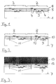
- a first component substrate 1 from e.g. Monocrystalline silicon comprises a plurality of, usually identical, chips 2 arranged according to a defined scheme, which contain circuit structures 3, such as, for example, a MOS transistor, and one or more metallization levels 4, which are typically made of aluminum, an aluminum alloy or other materials, such as copper or tungsten , exist and for electrical insulation are surrounded by an oxide layer 5, which can also be doped with boron and / or phosphorus for planarization purposes.
- the top metallization level 4 can also be covered by a passivation layer 6 made of, for example, silicon oxide and silicon nitride.
- adjustment structures for the precise joining of several levels are implemented (not shown in FIG. 1).
- the substrate has a thickness of e.g. 625 ⁇ m. This component substrate represents the lower substrate of the multilayer system (FIG. 1).
- a second component substrate 7 likewise comprises a plurality of, usually identical, chips 8 arranged according to a defined scheme, which contain circuit structures 9, such as a MOS transistor, and one or more metallization levels 10.
- This substrate 7 is constructed essentially similarly to the first component substrate 1, but the circuit structures 9 are generally different in their function.
- the second component substrate has via holes 11 at the points at which the electrical contact to the underlying circuit structures of the first substrate is to be made later. The via holes 11 are so deep that they extend to below the layer with circuit structures 9 (FIG. 2).
- the passivation is opened at the top metallization level at certain measuring points.
- the individual chips of the substrate are then subjected to a functional test and the defective chips are identified (for example with an ink jet). A passivation layer is then applied again in order to protect the exposed measuring points again.
- This adhesive layer 12 with a thickness of typically 1-2 ⁇ m can also cause a planarization of the surface.
- the auxiliary substrate 13 is used as a handling substrate for the further process steps and protects the surface of the component substrate 7 during further processing. (Fig. 3).
- the second component substrate 7 is thinned by etching and / or grinding from the back to the via holes 11, so that the thickness of the substrate 7 below the circuit structures 9 is only a few micrometers, typically 1-5 ⁇ m. The selected remaining thickness also depends on the type of circuits contained.
- the second component substrate 7 with the handling substrate 13 is divided into individual chips. This can be done with an etching process, by sawing or with a laser.
- the marked, intact chips are then applied to the first component substrate 1, provided with an adhesive layer 14, next to one another in an adjusted manner.
- the adhesive layer 14 with a thickness of typically 1-2 ⁇ m can cause a planarization of the surface.
- the handling substrates 13 are then removed, for example by etching or grinding, and the exposed adhesive layer 12 is typically removed over the entire area using an oxygen plasma or a solvent.
- the surface of the first substrate now has trenches between the individual chips, which have a very low aspect ratio. Through a planarization step in which the layer 15 is deposited, these trenches are now filled and a flat surface is created.
- the first component substrate 1 with the two component levels can now be further processed like a conventional silicon substrate with standard technology devices (FIG. 4).
- the vertical connection 16 is finally established between a metallization level 10 of the upper component level (substrate 7) and a metallization level 4 of the lower component level (substrate 1).
- a contact hole to a metallization level 10 of the upper component level and the prepared via holes 11 to a metallization level 4 of the lower component level are opened with a photolithography step and an electrical connection is realized by metal deposition and structuring.
- a passivation layer 17 is deposited on the surface (FIG. 5).
- the electrical contacting can of course also be implemented in other ways, e.g. already when the chips are applied to the lower substrate by means of prepared front and back contacts (see introduction to the description: Y. Hayashi et al.).
Applications Claiming Priority (2)
| Application Number | Priority Date | Filing Date | Title |
|---|---|---|---|
| DE4433845 | 1994-09-22 | ||
| DE4433845A DE4433845A1 (de) | 1994-09-22 | 1994-09-22 | Verfahren zur Herstellung einer dreidimensionalen integrierten Schaltung |
Publications (2)
| Publication Number | Publication Date |
|---|---|
| EP0703618A1 true EP0703618A1 (fr) | 1996-03-27 |
| EP0703618B1 EP0703618B1 (fr) | 2001-06-06 |
Family
ID=6528903
Family Applications (1)
| Application Number | Title | Priority Date | Filing Date |
|---|---|---|---|
| EP95113423A Expired - Lifetime EP0703618B1 (fr) | 1994-09-22 | 1995-08-26 | Procédé pour fabriquer un circuit intégré tridimensionnel |
Country Status (4)
| Country | Link |
|---|---|
| US (1) | US5563084A (fr) |
| EP (1) | EP0703618B1 (fr) |
| JP (1) | JP3986575B2 (fr) |
| DE (2) | DE4433845A1 (fr) |
Cited By (7)
| Publication number | Priority date | Publication date | Assignee | Title |
|---|---|---|---|---|
| EP0975472A1 (fr) * | 1997-04-04 | 2000-02-02 | Glenn J. Leedy | Memoire a structure tridimensionnelle |
| WO2000074136A1 (fr) * | 1999-05-31 | 2000-12-07 | Fraunhofer-Gesellschaft zur Förderung der angewandten Forschung e.V. | Procede de production de circuits tridimensionnels |
| DE10323394A1 (de) * | 2003-05-20 | 2004-12-23 | Fraunhofer-Gesellschaft zur Förderung der angewandten Forschung e.V. | Verfahren und Vorrichtung zum Erzeugen einer elektrischen Kontaktierung zwischen zwei Halbleiterstücken und Anordnung von Halbleiterstücken |
| EP1564807A2 (fr) | 2004-02-17 | 2005-08-17 | Sanyo Electric Co., Ltd. | Composant semiconducteur et méthode de fabrication |
| DE102004056970A1 (de) * | 2004-11-25 | 2006-06-01 | Fraunhofer-Gesellschaft zur Förderung der angewandten Forschung e.V. | Verfahren und Vorrichtung zum Erzeugen einer elektrischen Kontaktierung zwischen zwei Halbleiterstücken durch ein mechanisches Element |
| US7670893B2 (en) | 1992-04-08 | 2010-03-02 | Taiwan Semiconductor Manufacturing Co., Ltd. | Membrane IC fabrication |
| US7705466B2 (en) | 1997-04-04 | 2010-04-27 | Elm Technology Corporation | Three dimensional multi layer memory and control logic integrated circuit structure |
Families Citing this family (316)
| Publication number | Priority date | Publication date | Assignee | Title |
|---|---|---|---|---|
| US5665649A (en) * | 1993-05-21 | 1997-09-09 | Gardiner Communications Corporation | Process for forming a semiconductor device base array and mounting semiconductor devices thereon |
| DE4433846C2 (de) * | 1994-09-22 | 1999-06-02 | Fraunhofer Ges Forschung | Verfahren zur Herstellung einer vertikalen integrierten Schaltungsstruktur |
| DE19516487C1 (de) * | 1995-05-05 | 1996-07-25 | Fraunhofer Ges Forschung | Verfahren zur vertikalen Integration mikroelektronischer Systeme |
| DE19543540C1 (de) | 1995-11-22 | 1996-11-21 | Siemens Ag | Vertikal integriertes Halbleiterbauelement mit zwei miteinander verbundenen Substraten und Herstellungsverfahren dafür |
| US5851845A (en) * | 1995-12-18 | 1998-12-22 | Micron Technology, Inc. | Process for packaging a semiconductor die using dicing and testing |
| US5817530A (en) * | 1996-05-20 | 1998-10-06 | Micron Technology, Inc. | Use of conductive lines on the back side of wafers and dice for semiconductor interconnects |
| US8018058B2 (en) * | 2004-06-21 | 2011-09-13 | Besang Inc. | Semiconductor memory device |
| KR100904771B1 (ko) | 2003-06-24 | 2009-06-26 | 이상윤 | 3차원 집적회로 구조 및 제작 방법 |
| US7888764B2 (en) * | 2003-06-24 | 2011-02-15 | Sang-Yun Lee | Three-dimensional integrated circuit structure |
| US20050280155A1 (en) * | 2004-06-21 | 2005-12-22 | Sang-Yun Lee | Semiconductor bonding and layer transfer method |
| US8058142B2 (en) * | 1996-11-04 | 2011-11-15 | Besang Inc. | Bonded semiconductor structure and method of making the same |
| WO1999016131A1 (fr) * | 1997-09-19 | 1999-04-01 | Fraunhofer-Gesellschaft zur Förderung der angewandten Forschung e.V. | Procede de cablage pour composants a semi-conducteur destines a empecher le piratage et la manipulation des produits, composant a semi-conducteur produit selon ce procede et utilisation du composant a semi-conducteur dans une carte a puce |
| DE19746641B4 (de) * | 1997-09-19 | 2006-02-23 | Fraunhofer-Gesellschaft zur Förderung der angewandten Forschung e.V. | Verdrahtungsverfahren für Halbleiter-Bauelemente zur Verhinderung von Produktpiraterie und Produktmanipulation und Verwendung des Halbleiter-Bauelements in einer Chipkarte |
| DE19746642C2 (de) * | 1997-10-22 | 2002-07-18 | Fraunhofer Ges Forschung | Verfahren zur Herstellung eines Halbleiterbauelements sowie dessen Verwendung in einer Chipkarte |
| DE19748666C2 (de) * | 1997-11-04 | 2002-08-29 | Fraunhofer Ges Forschung | Verdrahtungsverfahren für mikroelektronische Systeme zur Verhinderung von Produktpiraterie und Produktmanipulation, durch das Verfahren hergestelltes mikroelektronisches System und Verwendung des mikroelektronischen Systems in einer Chipkarte |
| DE19750316A1 (de) * | 1997-11-13 | 1999-05-27 | Siemens Ag | Siliziumfolie als Träger von Halbleiterschaltungen als Teil von Karten |
| US6275297B1 (en) | 1998-08-19 | 2001-08-14 | Sc Technology | Method of measuring depths of structures on a semiconductor substrate |
| DE19838439C1 (de) * | 1998-08-24 | 2000-04-27 | Fraunhofer Ges Forschung | Dünnfilmphotodiode und Verfahren zur Herstellung |
| EP1116180B1 (fr) | 1998-09-03 | 2002-10-02 | Fraunhofer-Gesellschaft Zur Förderung Der Angewandten Forschung E.V. | Procede de collage d'une puce de circuit |
| DE19849586C1 (de) * | 1998-10-27 | 2000-05-11 | Fraunhofer Ges Forschung | Verfahren zum Herstellen dreidimensionaler Schaltungen |
| DE19853703A1 (de) | 1998-11-20 | 2000-05-25 | Giesecke & Devrient Gmbh | Verfahren zur Herstellung eines beidseitig prozessierten integrierten Schaltkreises |
| DE19856573C1 (de) | 1998-12-08 | 2000-05-18 | Fraunhofer Ges Forschung | Verfahren zur vertikalen Integration von aktiven Schaltungsebenen und unter Verwendung desselben erzeugte vertikale integrierte Schaltung |
| DE19918671B4 (de) * | 1999-04-23 | 2006-03-02 | Giesecke & Devrient Gmbh | Vertikal integrierbare Schaltung und Verfahren zu ihrer Herstellung |
| EP1171912B1 (fr) | 1999-05-27 | 2003-09-24 | Fraunhofer-Gesellschaft zur Förderung der angewandten Forschung e.V. | Procede d'integration verticale de composants electriques a l'aide d'un contact arriere |
| US7582490B2 (en) | 1999-06-22 | 2009-09-01 | President And Fellows Of Harvard College | Controlled fabrication of gaps in electrically conducting structures |
| US6783643B2 (en) | 1999-06-22 | 2004-08-31 | President And Fellows Of Harvard College | Control of solid state dimensional features |
| AU5763000A (en) * | 1999-06-22 | 2001-01-09 | President And Fellows Of Harvard College | Molecular and atomic scale evaluation of biopolymers |
| US7118657B2 (en) | 1999-06-22 | 2006-10-10 | President And Fellows Of Harvard College | Pulsed ion beam control of solid state features |
| US7258838B2 (en) | 1999-06-22 | 2007-08-21 | President And Fellows Of Harvard College | Solid state molecular probe device |
| US6464842B1 (en) | 1999-06-22 | 2002-10-15 | President And Fellows Of Harvard College | Control of solid state dimensional features |
| US6650426B1 (en) | 1999-07-12 | 2003-11-18 | Sc Technology, Inc. | Endpoint determination for recess etching to a precise depth |
| DE19933472A1 (de) * | 1999-07-20 | 2001-02-01 | Daimler Chrysler Ag | Netzwerk zur Signalverarbeitung, insbesondere zur Bilddatenverarbeitung, und Bildaufnahmesystem |
| US6500694B1 (en) * | 2000-03-22 | 2002-12-31 | Ziptronix, Inc. | Three dimensional device integration method and integrated device |
| US6984571B1 (en) * | 1999-10-01 | 2006-01-10 | Ziptronix, Inc. | Three dimensional device integration method and integrated device |
| US6902987B1 (en) | 2000-02-16 | 2005-06-07 | Ziptronix, Inc. | Method for low temperature bonding and bonded structure |
| DE10008386A1 (de) * | 2000-02-23 | 2001-08-30 | Giesecke & Devrient Gmbh | Verfahren zum Verbinden von Substraten einer vertikal integrierten Schaltungsstruktur |
| US6563133B1 (en) | 2000-08-09 | 2003-05-13 | Ziptronix, Inc. | Method of epitaxial-like wafer bonding at low temperature and bonded structure |
| US6674161B1 (en) * | 2000-10-03 | 2004-01-06 | Rambus Inc. | Semiconductor stacked die devices |
| EP1195808B1 (fr) | 2000-10-04 | 2007-08-15 | Infineon Technologies AG | Méthode de fabrication d'une couche mince de dispositifs semi-conducteurs autoportée et de réalisation d'un circuit intégré à trois dimensions |
| EP1215721B1 (fr) * | 2000-12-13 | 2008-01-23 | Infineon Technologies AG | Procédé pour le traitement en plusieurs étapes d'une plaquette semiconductrice mince et cassante |
| US6748994B2 (en) | 2001-04-11 | 2004-06-15 | Avery Dennison Corporation | Label applicator, method and label therefor |
| KR100394808B1 (ko) * | 2001-07-19 | 2003-08-14 | 삼성전자주식회사 | 웨이퍼 레벨 적층 칩 패키지 및 그 제조 방법 |
| DE10164800B4 (de) | 2001-11-02 | 2005-03-31 | Infineon Technologies Ag | Verfahren zur Herstellung eines elektronischen Bauelements mit mehreren übereinander gestapelten und miteinander kontaktierten Chips |
| DE10153609C2 (de) * | 2001-11-02 | 2003-10-16 | Infineon Technologies Ag | Verfahren zur Herstellung eines elektronischen Bauelements mit mehreren übereinander gestapelten und miteinander kontaktierten Chips |
| DE10200399B4 (de) * | 2002-01-08 | 2008-03-27 | Advanced Micro Devices, Inc., Sunnyvale | Verfahren zur Erzeugung einer dreidimensional integrierten Halbleitervorrichtung und dreidimensional integrierte Halbleitervorrichtung |
| EP1367645A3 (fr) * | 2002-05-31 | 2006-12-27 | Fujitsu Limited | Dispositif semi-conducteur et méthode de fabrication associée |
| TWI234253B (en) * | 2002-05-31 | 2005-06-11 | Fujitsu Ltd | Semiconductor device and manufacturing method thereof |
| US7402897B2 (en) | 2002-08-08 | 2008-07-22 | Elm Technology Corporation | Vertical system integration |
| US7064055B2 (en) * | 2002-12-31 | 2006-06-20 | Massachusetts Institute Of Technology | Method of forming a multi-layer semiconductor structure having a seamless bonding interface |
| WO2004061961A1 (fr) * | 2002-12-31 | 2004-07-22 | Massachusetts Institute Of Technology | Structure integree multicouche de semi-conducteur avec partie d'ecran electrique |
| US20100133695A1 (en) * | 2003-01-12 | 2010-06-03 | Sang-Yun Lee | Electronic circuit with embedded memory |
| US6770495B1 (en) * | 2003-01-15 | 2004-08-03 | Advanced Micro Devices, Inc. | Method for revealing active regions in a SOI structure for DUT backside inspection |
| US6962835B2 (en) | 2003-02-07 | 2005-11-08 | Ziptronix, Inc. | Method for room temperature metal direct bonding |
| US7109092B2 (en) | 2003-05-19 | 2006-09-19 | Ziptronix, Inc. | Method of room temperature covalent bonding |
| JP4819320B2 (ja) * | 2003-05-28 | 2011-11-24 | 株式会社オクテック | 半導体装置の製造方法 |
| US8071438B2 (en) * | 2003-06-24 | 2011-12-06 | Besang Inc. | Semiconductor circuit |
| US20100190334A1 (en) * | 2003-06-24 | 2010-07-29 | Sang-Yun Lee | Three-dimensional semiconductor structure and method of manufacturing the same |
| DE10342980B3 (de) * | 2003-09-17 | 2005-01-05 | Disco Hi-Tec Europe Gmbh | Verfahren zur Bildung von Chip-Stapeln |
| JP2005123463A (ja) | 2003-10-17 | 2005-05-12 | Seiko Epson Corp | 半導体装置及びその製造方法、半導体装置モジュール、回路基板並びに電子機器 |
| JP5354765B2 (ja) * | 2004-08-20 | 2013-11-27 | カミヤチョウ アイピー ホールディングス | 三次元積層構造を持つ半導体装置の製造方法 |
| US8392021B2 (en) | 2005-02-18 | 2013-03-05 | Irobot Corporation | Autonomous surface cleaning robot for wet cleaning |
| US20110143506A1 (en) * | 2009-12-10 | 2011-06-16 | Sang-Yun Lee | Method for fabricating a semiconductor memory device |
| US8367524B2 (en) * | 2005-03-29 | 2013-02-05 | Sang-Yun Lee | Three-dimensional integrated circuit structure |
| US20110001172A1 (en) * | 2005-03-29 | 2011-01-06 | Sang-Yun Lee | Three-dimensional integrated circuit structure |
| US7462552B2 (en) * | 2005-05-23 | 2008-12-09 | Ziptronix, Inc. | Method of detachable direct bonding at low temperatures |
| US8456015B2 (en) | 2005-06-14 | 2013-06-04 | Cufer Asset Ltd. L.L.C. | Triaxial through-chip connection |
| US7534722B2 (en) | 2005-06-14 | 2009-05-19 | John Trezza | Back-to-front via process |
| US7851348B2 (en) | 2005-06-14 | 2010-12-14 | Abhay Misra | Routingless chip architecture |
| US7838997B2 (en) | 2005-06-14 | 2010-11-23 | John Trezza | Remote chip attachment |
| US7560813B2 (en) | 2005-06-14 | 2009-07-14 | John Trezza | Chip-based thermo-stack |
| US7969015B2 (en) | 2005-06-14 | 2011-06-28 | Cufer Asset Ltd. L.L.C. | Inverse chip connector |
| US7521806B2 (en) * | 2005-06-14 | 2009-04-21 | John Trezza | Chip spanning connection |
| US7687400B2 (en) | 2005-06-14 | 2010-03-30 | John Trezza | Side stacking apparatus and method |
| US7786592B2 (en) * | 2005-06-14 | 2010-08-31 | John Trezza | Chip capacitive coupling |
| US7767493B2 (en) | 2005-06-14 | 2010-08-03 | John Trezza | Post & penetration interconnection |
| US7781886B2 (en) | 2005-06-14 | 2010-08-24 | John Trezza | Electronic chip contact structure |
| US7776715B2 (en) * | 2005-07-26 | 2010-08-17 | Micron Technology, Inc. | Reverse construction memory cell |
| US7622313B2 (en) * | 2005-07-29 | 2009-11-24 | Freescale Semiconductor, Inc. | Fabrication of three dimensional integrated circuit employing multiple die panels |
| US7485968B2 (en) * | 2005-08-11 | 2009-02-03 | Ziptronix, Inc. | 3D IC method and device |
| US20070106317A1 (en) | 2005-11-09 | 2007-05-10 | Shelton Frederick E Iv | Hydraulically and electrically actuated articulation joints for surgical instruments |
| US7378339B2 (en) * | 2006-03-30 | 2008-05-27 | Freescale Semiconductor, Inc. | Barrier for use in 3-D integration of circuits |
| US7687397B2 (en) | 2006-06-06 | 2010-03-30 | John Trezza | Front-end processed wafer having through-chip connections |
| US8513789B2 (en) * | 2006-10-10 | 2013-08-20 | Tessera, Inc. | Edge connect wafer level stacking with leads extending along edges |
| US7901989B2 (en) * | 2006-10-10 | 2011-03-08 | Tessera, Inc. | Reconstituted wafer level stacking |
| US7829438B2 (en) * | 2006-10-10 | 2010-11-09 | Tessera, Inc. | Edge connect wafer level stacking |
| KR101175393B1 (ko) * | 2006-10-17 | 2012-08-20 | 쿠퍼 에셋 엘티디. 엘.엘.씨. | 웨이퍼 비아 형성 |
| US7952195B2 (en) * | 2006-12-28 | 2011-05-31 | Tessera, Inc. | Stacked packages with bridging traces |
| US7705613B2 (en) * | 2007-01-03 | 2010-04-27 | Abhay Misra | Sensitivity capacitive sensor |
| US7670874B2 (en) | 2007-02-16 | 2010-03-02 | John Trezza | Plated pillar package formation |
| US7850060B2 (en) * | 2007-04-05 | 2010-12-14 | John Trezza | Heat cycle-able connection |
| US7748116B2 (en) * | 2007-04-05 | 2010-07-06 | John Trezza | Mobile binding in an electronic connection |
| US7960210B2 (en) * | 2007-04-23 | 2011-06-14 | Cufer Asset Ltd. L.L.C. | Ultra-thin chip packaging |
| US8367471B2 (en) | 2007-06-15 | 2013-02-05 | Micron Technology, Inc. | Semiconductor assemblies, stacked semiconductor devices, and methods of manufacturing semiconductor assemblies and stacked semiconductor devices |
| US8461672B2 (en) * | 2007-07-27 | 2013-06-11 | Tessera, Inc. | Reconstituted wafer stack packaging with after-applied pad extensions |
| US8193092B2 (en) | 2007-07-31 | 2012-06-05 | Micron Technology, Inc. | Semiconductor devices including a through-substrate conductive member with an exposed end and methods of manufacturing such semiconductor devices |
| KR101533663B1 (ko) | 2007-08-03 | 2015-07-03 | 테세라, 인코포레이티드 | 재구성된 웨이퍼를 이용한 스택 패키지 |
| US8043895B2 (en) | 2007-08-09 | 2011-10-25 | Tessera, Inc. | Method of fabricating stacked assembly including plurality of stacked microelectronic elements |
| CN102067310B (zh) * | 2008-06-16 | 2013-08-21 | 泰塞拉公司 | 带有边缘触头的晶片级芯片规模封装的堆叠及其制造方法 |
| CN102422412A (zh) * | 2009-03-13 | 2012-04-18 | 德塞拉股份有限公司 | 具有穿过结合垫延伸的通路的堆叠式微电子组件 |
| US8669778B1 (en) | 2009-04-14 | 2014-03-11 | Monolithic 3D Inc. | Method for design and manufacturing of a 3D semiconductor device |
| US8754533B2 (en) | 2009-04-14 | 2014-06-17 | Monolithic 3D Inc. | Monolithic three-dimensional semiconductor device and structure |
| US9711407B2 (en) | 2009-04-14 | 2017-07-18 | Monolithic 3D Inc. | Method of manufacturing a three dimensional integrated circuit by transfer of a mono-crystalline layer |
| US8384426B2 (en) | 2009-04-14 | 2013-02-26 | Monolithic 3D Inc. | Semiconductor device and structure |
| US8373439B2 (en) | 2009-04-14 | 2013-02-12 | Monolithic 3D Inc. | 3D semiconductor device |
| US8427200B2 (en) | 2009-04-14 | 2013-04-23 | Monolithic 3D Inc. | 3D semiconductor device |
| US8405420B2 (en) | 2009-04-14 | 2013-03-26 | Monolithic 3D Inc. | System comprising a semiconductor device and structure |
| US9577642B2 (en) | 2009-04-14 | 2017-02-21 | Monolithic 3D Inc. | Method to form a 3D semiconductor device |
| US7986042B2 (en) | 2009-04-14 | 2011-07-26 | Monolithic 3D Inc. | Method for fabrication of a semiconductor device and structure |
| US8395191B2 (en) | 2009-10-12 | 2013-03-12 | Monolithic 3D Inc. | Semiconductor device and structure |
| US9509313B2 (en) | 2009-04-14 | 2016-11-29 | Monolithic 3D Inc. | 3D semiconductor device |
| US8362482B2 (en) | 2009-04-14 | 2013-01-29 | Monolithic 3D Inc. | Semiconductor device and structure |
| US8378715B2 (en) | 2009-04-14 | 2013-02-19 | Monolithic 3D Inc. | Method to construct systems |
| US8058137B1 (en) | 2009-04-14 | 2011-11-15 | Monolithic 3D Inc. | Method for fabrication of a semiconductor device and structure |
| US8362800B2 (en) | 2010-10-13 | 2013-01-29 | Monolithic 3D Inc. | 3D semiconductor device including field repairable logics |
| US8536023B2 (en) | 2010-11-22 | 2013-09-17 | Monolithic 3D Inc. | Method of manufacturing a semiconductor device and structure |
| US11018133B2 (en) | 2009-10-12 | 2021-05-25 | Monolithic 3D Inc. | 3D integrated circuit |
| US10354995B2 (en) | 2009-10-12 | 2019-07-16 | Monolithic 3D Inc. | Semiconductor memory device and structure |
| US10910364B2 (en) | 2009-10-12 | 2021-02-02 | Monolitaic 3D Inc. | 3D semiconductor device |
| US10043781B2 (en) | 2009-10-12 | 2018-08-07 | Monolithic 3D Inc. | 3D semiconductor device and structure |
| US8476145B2 (en) | 2010-10-13 | 2013-07-02 | Monolithic 3D Inc. | Method of fabricating a semiconductor device and structure |
| US10366970B2 (en) | 2009-10-12 | 2019-07-30 | Monolithic 3D Inc. | 3D semiconductor device and structure |
| US8581349B1 (en) | 2011-05-02 | 2013-11-12 | Monolithic 3D Inc. | 3D memory semiconductor device and structure |
| US10157909B2 (en) | 2009-10-12 | 2018-12-18 | Monolithic 3D Inc. | 3D semiconductor device and structure |
| US11374118B2 (en) | 2009-10-12 | 2022-06-28 | Monolithic 3D Inc. | Method to form a 3D integrated circuit |
| US8294159B2 (en) | 2009-10-12 | 2012-10-23 | Monolithic 3D Inc. | Method for fabrication of a semiconductor device and structure |
| US9099424B1 (en) | 2012-08-10 | 2015-08-04 | Monolithic 3D Inc. | Semiconductor system, device and structure with heat removal |
| US8742476B1 (en) | 2012-11-27 | 2014-06-03 | Monolithic 3D Inc. | Semiconductor device and structure |
| US8450804B2 (en) | 2011-03-06 | 2013-05-28 | Monolithic 3D Inc. | Semiconductor device and structure for heat removal |
| US10388863B2 (en) | 2009-10-12 | 2019-08-20 | Monolithic 3D Inc. | 3D memory device and structure |
| US8841777B2 (en) * | 2010-01-12 | 2014-09-23 | International Business Machines Corporation | Bonded structure employing metal semiconductor alloy bonding |
| US8492886B2 (en) | 2010-02-16 | 2013-07-23 | Monolithic 3D Inc | 3D integrated circuit with logic |
| US8026521B1 (en) | 2010-10-11 | 2011-09-27 | Monolithic 3D Inc. | Semiconductor device and structure |
| US8373230B1 (en) | 2010-10-13 | 2013-02-12 | Monolithic 3D Inc. | Method for fabrication of a semiconductor device and structure |
| US8461035B1 (en) | 2010-09-30 | 2013-06-11 | Monolithic 3D Inc. | Method for fabrication of a semiconductor device and structure |
| US8541819B1 (en) | 2010-12-09 | 2013-09-24 | Monolithic 3D Inc. | Semiconductor device and structure |
| US9099526B2 (en) | 2010-02-16 | 2015-08-04 | Monolithic 3D Inc. | Integrated circuit device and structure |
| US8288795B2 (en) | 2010-03-02 | 2012-10-16 | Micron Technology, Inc. | Thyristor based memory cells, devices and systems including the same and methods for forming the same |
| US9608119B2 (en) | 2010-03-02 | 2017-03-28 | Micron Technology, Inc. | Semiconductor-metal-on-insulator structures, methods of forming such structures, and semiconductor devices including such structures |
| US8513722B2 (en) | 2010-03-02 | 2013-08-20 | Micron Technology, Inc. | Floating body cell structures, devices including same, and methods for forming same |
| US9646869B2 (en) * | 2010-03-02 | 2017-05-09 | Micron Technology, Inc. | Semiconductor devices including a diode structure over a conductive strap and methods of forming such semiconductor devices |
| US8507966B2 (en) | 2010-03-02 | 2013-08-13 | Micron Technology, Inc. | Semiconductor cells, arrays, devices and systems having a buried conductive line and methods for forming the same |
| US8525342B2 (en) * | 2010-04-12 | 2013-09-03 | Qualcomm Incorporated | Dual-side interconnected CMOS for stacked integrated circuits |
| KR101134819B1 (ko) | 2010-07-02 | 2012-04-13 | 이상윤 | 반도체 메모리 장치의 제조 방법 |
| US9219005B2 (en) | 2011-06-28 | 2015-12-22 | Monolithic 3D Inc. | Semiconductor system and device |
| US9953925B2 (en) | 2011-06-28 | 2018-04-24 | Monolithic 3D Inc. | Semiconductor system and device |
| US10217667B2 (en) | 2011-06-28 | 2019-02-26 | Monolithic 3D Inc. | 3D semiconductor device, fabrication method and system |
| US8642416B2 (en) | 2010-07-30 | 2014-02-04 | Monolithic 3D Inc. | Method of forming three dimensional integrated circuit devices using layer transfer technique |
| US8901613B2 (en) | 2011-03-06 | 2014-12-02 | Monolithic 3D Inc. | Semiconductor device and structure for heat removal |
| US8163581B1 (en) | 2010-10-13 | 2012-04-24 | Monolith IC 3D | Semiconductor and optoelectronic devices |
| US8273610B2 (en) | 2010-11-18 | 2012-09-25 | Monolithic 3D Inc. | Method of constructing a semiconductor device and structure |
| US10497713B2 (en) | 2010-11-18 | 2019-12-03 | Monolithic 3D Inc. | 3D semiconductor memory device and structure |
| US11482440B2 (en) | 2010-12-16 | 2022-10-25 | Monolithic 3D Inc. | 3D semiconductor device and structure with a built-in test circuit for repairing faulty circuits |
| US10290682B2 (en) | 2010-10-11 | 2019-05-14 | Monolithic 3D Inc. | 3D IC semiconductor device and structure with stacked memory |
| US8114757B1 (en) | 2010-10-11 | 2012-02-14 | Monolithic 3D Inc. | Semiconductor device and structure |
| US11469271B2 (en) | 2010-10-11 | 2022-10-11 | Monolithic 3D Inc. | Method to produce 3D semiconductor devices and structures with memory |
| US11227897B2 (en) | 2010-10-11 | 2022-01-18 | Monolithic 3D Inc. | Method for producing a 3D semiconductor memory device and structure |
| US11257867B1 (en) | 2010-10-11 | 2022-02-22 | Monolithic 3D Inc. | 3D semiconductor device and structure with oxide bonds |
| US11315980B1 (en) | 2010-10-11 | 2022-04-26 | Monolithic 3D Inc. | 3D semiconductor device and structure with transistors |
| US11018191B1 (en) | 2010-10-11 | 2021-05-25 | Monolithic 3D Inc. | 3D semiconductor device and structure |
| US11158674B2 (en) | 2010-10-11 | 2021-10-26 | Monolithic 3D Inc. | Method to produce a 3D semiconductor device and structure |
| US10896931B1 (en) | 2010-10-11 | 2021-01-19 | Monolithic 3D Inc. | 3D semiconductor device and structure |
| US11024673B1 (en) | 2010-10-11 | 2021-06-01 | Monolithic 3D Inc. | 3D semiconductor device and structure |
| US11600667B1 (en) | 2010-10-11 | 2023-03-07 | Monolithic 3D Inc. | Method to produce 3D semiconductor devices and structures with memory |
| US10833108B2 (en) | 2010-10-13 | 2020-11-10 | Monolithic 3D Inc. | 3D microdisplay device and structure |
| US11855100B2 (en) | 2010-10-13 | 2023-12-26 | Monolithic 3D Inc. | Multilevel semiconductor device and structure with oxide bonding |
| US11855114B2 (en) | 2010-10-13 | 2023-12-26 | Monolithic 3D Inc. | Multilevel semiconductor device and structure with image sensors and wafer bonding |
| US11929372B2 (en) | 2010-10-13 | 2024-03-12 | Monolithic 3D Inc. | Multilevel semiconductor device and structure with image sensors and wafer bonding |
| US10943934B2 (en) | 2010-10-13 | 2021-03-09 | Monolithic 3D Inc. | Multilevel semiconductor device and structure |
| US10998374B1 (en) | 2010-10-13 | 2021-05-04 | Monolithic 3D Inc. | Multilevel semiconductor device and structure |
| US10978501B1 (en) | 2010-10-13 | 2021-04-13 | Monolithic 3D Inc. | Multilevel semiconductor device and structure with waveguides |
| US11869915B2 (en) | 2010-10-13 | 2024-01-09 | Monolithic 3D Inc. | Multilevel semiconductor device and structure with image sensors and wafer bonding |
| US11163112B2 (en) | 2010-10-13 | 2021-11-02 | Monolithic 3D Inc. | Multilevel semiconductor device and structure with electromagnetic modulators |
| US11437368B2 (en) | 2010-10-13 | 2022-09-06 | Monolithic 3D Inc. | Multilevel semiconductor device and structure with oxide bonding |
| US11327227B2 (en) | 2010-10-13 | 2022-05-10 | Monolithic 3D Inc. | Multilevel semiconductor device and structure with electromagnetic modulators |
| US9197804B1 (en) | 2011-10-14 | 2015-11-24 | Monolithic 3D Inc. | Semiconductor and optoelectronic devices |
| US8379458B1 (en) | 2010-10-13 | 2013-02-19 | Monolithic 3D Inc. | Semiconductor device and structure |
| US11063071B1 (en) | 2010-10-13 | 2021-07-13 | Monolithic 3D Inc. | Multilevel semiconductor device and structure with waveguides |
| US11404466B2 (en) | 2010-10-13 | 2022-08-02 | Monolithic 3D Inc. | Multilevel semiconductor device and structure with image sensors |
| US11605663B2 (en) | 2010-10-13 | 2023-03-14 | Monolithic 3D Inc. | Multilevel semiconductor device and structure with image sensors and wafer bonding |
| US11694922B2 (en) | 2010-10-13 | 2023-07-04 | Monolithic 3D Inc. | Multilevel semiconductor device and structure with oxide bonding |
| US11133344B2 (en) | 2010-10-13 | 2021-09-28 | Monolithic 3D Inc. | Multilevel semiconductor device and structure with image sensors |
| US11164898B2 (en) | 2010-10-13 | 2021-11-02 | Monolithic 3D Inc. | Multilevel semiconductor device and structure |
| US10679977B2 (en) | 2010-10-13 | 2020-06-09 | Monolithic 3D Inc. | 3D microdisplay device and structure |
| US11043523B1 (en) | 2010-10-13 | 2021-06-22 | Monolithic 3D Inc. | Multilevel semiconductor device and structure with image sensors |
| US9064881B2 (en) * | 2010-11-11 | 2015-06-23 | Taiwan Semiconductor Manufacturing Company, Ltd. | Protecting flip-chip package using pre-applied fillet |
| US11121021B2 (en) | 2010-11-18 | 2021-09-14 | Monolithic 3D Inc. | 3D semiconductor device and structure |
| US11862503B2 (en) | 2010-11-18 | 2024-01-02 | Monolithic 3D Inc. | Method for producing a 3D semiconductor device and structure with memory cells and multiple metal layers |
| US11482438B2 (en) | 2010-11-18 | 2022-10-25 | Monolithic 3D Inc. | Methods for producing a 3D semiconductor memory device and structure |
| US11164770B1 (en) | 2010-11-18 | 2021-11-02 | Monolithic 3D Inc. | Method for producing a 3D semiconductor memory device and structure |
| US11443971B2 (en) | 2010-11-18 | 2022-09-13 | Monolithic 3D Inc. | 3D semiconductor device and structure with memory |
| US11610802B2 (en) | 2010-11-18 | 2023-03-21 | Monolithic 3D Inc. | Method for producing a 3D semiconductor device and structure with single crystal transistors and metal gate electrodes |
| US11355380B2 (en) | 2010-11-18 | 2022-06-07 | Monolithic 3D Inc. | Methods for producing 3D semiconductor memory device and structure utilizing alignment marks |
| US11018042B1 (en) | 2010-11-18 | 2021-05-25 | Monolithic 3D Inc. | 3D semiconductor memory device and structure |
| US11804396B2 (en) | 2010-11-18 | 2023-10-31 | Monolithic 3D Inc. | Methods for producing a 3D semiconductor device and structure with memory cells and multiple metal layers |
| US11569117B2 (en) | 2010-11-18 | 2023-01-31 | Monolithic 3D Inc. | 3D semiconductor device and structure with single-crystal layers |
| US11615977B2 (en) | 2010-11-18 | 2023-03-28 | Monolithic 3D Inc. | 3D semiconductor memory device and structure |
| US11784082B2 (en) | 2010-11-18 | 2023-10-10 | Monolithic 3D Inc. | 3D semiconductor device and structure with bonding |
| US11482439B2 (en) | 2010-11-18 | 2022-10-25 | Monolithic 3D Inc. | Methods for producing a 3D semiconductor memory device comprising charge trap junction-less transistors |
| US11735462B2 (en) | 2010-11-18 | 2023-08-22 | Monolithic 3D Inc. | 3D semiconductor device and structure with single-crystal layers |
| US11508605B2 (en) | 2010-11-18 | 2022-11-22 | Monolithic 3D Inc. | 3D semiconductor memory device and structure |
| US11107721B2 (en) | 2010-11-18 | 2021-08-31 | Monolithic 3D Inc. | 3D semiconductor device and structure with NAND logic |
| US11854857B1 (en) | 2010-11-18 | 2023-12-26 | Monolithic 3D Inc. | Methods for producing a 3D semiconductor device and structure with memory cells and multiple metal layers |
| US11004719B1 (en) | 2010-11-18 | 2021-05-11 | Monolithic 3D Inc. | Methods for producing a 3D semiconductor memory device and structure |
| US11211279B2 (en) | 2010-11-18 | 2021-12-28 | Monolithic 3D Inc. | Method for processing a 3D integrated circuit and structure |
| US11094576B1 (en) | 2010-11-18 | 2021-08-17 | Monolithic 3D Inc. | Methods for producing a 3D semiconductor memory device and structure |
| US11355381B2 (en) | 2010-11-18 | 2022-06-07 | Monolithic 3D Inc. | 3D semiconductor memory device and structure |
| US11031275B2 (en) | 2010-11-18 | 2021-06-08 | Monolithic 3D Inc. | 3D semiconductor device and structure with memory |
| US11521888B2 (en) | 2010-11-18 | 2022-12-06 | Monolithic 3D Inc. | 3D semiconductor device and structure with high-k metal gate transistors |
| US11495484B2 (en) | 2010-11-18 | 2022-11-08 | Monolithic 3D Inc. | 3D semiconductor devices and structures with at least two single-crystal layers |
| US11923230B1 (en) | 2010-11-18 | 2024-03-05 | Monolithic 3D Inc. | 3D semiconductor device and structure with bonding |
| US11901210B2 (en) | 2010-11-18 | 2024-02-13 | Monolithic 3D Inc. | 3D semiconductor device and structure with memory |
| US8598621B2 (en) | 2011-02-11 | 2013-12-03 | Micron Technology, Inc. | Memory cells, memory arrays, methods of forming memory cells, and methods of forming a shared doped semiconductor region of a vertically oriented thyristor and a vertically oriented access transistor |
| US8952418B2 (en) | 2011-03-01 | 2015-02-10 | Micron Technology, Inc. | Gated bipolar junction transistors |
| US8975670B2 (en) | 2011-03-06 | 2015-03-10 | Monolithic 3D Inc. | Semiconductor device and structure for heat removal |
| US8519431B2 (en) | 2011-03-08 | 2013-08-27 | Micron Technology, Inc. | Thyristors |
| CN103503122B (zh) | 2011-05-24 | 2016-05-18 | 索尼公司 | 半导体装置 |
| US10388568B2 (en) | 2011-06-28 | 2019-08-20 | Monolithic 3D Inc. | 3D semiconductor device and system |
| US8772848B2 (en) | 2011-07-26 | 2014-07-08 | Micron Technology, Inc. | Circuit structures, memory circuitry, and methods |
| US8687399B2 (en) | 2011-10-02 | 2014-04-01 | Monolithic 3D Inc. | Semiconductor device and structure |
| US9029173B2 (en) | 2011-10-18 | 2015-05-12 | Monolithic 3D Inc. | Method for fabrication of a semiconductor device and structure |
| DE102012200258A1 (de) | 2012-01-10 | 2013-07-11 | Fraunhofer-Gesellschaft zur Förderung der angewandten Forschung e.V. | Verfahren zur herstellung eines chips |
| US9000557B2 (en) | 2012-03-17 | 2015-04-07 | Zvi Or-Bach | Semiconductor device and structure |
| US11735501B1 (en) | 2012-04-09 | 2023-08-22 | Monolithic 3D Inc. | 3D semiconductor device and structure with metal layers and a connective path |
| US9954080B2 (en) * | 2012-04-09 | 2018-04-24 | Monolithic 3D Inc. | 3D integrated circuit device |
| US11410912B2 (en) | 2012-04-09 | 2022-08-09 | Monolithic 3D Inc. | 3D semiconductor device with vias and isolation layers |
| US8557632B1 (en) * | 2012-04-09 | 2013-10-15 | Monolithic 3D Inc. | Method for fabrication of a semiconductor device and structure |
| US11164811B2 (en) | 2012-04-09 | 2021-11-02 | Monolithic 3D Inc. | 3D semiconductor device with isolation layers and oxide-to-oxide bonding |
| US11088050B2 (en) | 2012-04-09 | 2021-08-10 | Monolithic 3D Inc. | 3D semiconductor device with isolation layers |
| US11616004B1 (en) | 2012-04-09 | 2023-03-28 | Monolithic 3D Inc. | 3D semiconductor device and structure with metal layers and a connective path |
| US9691869B2 (en) * | 2012-04-09 | 2017-06-27 | Monolithic 3D Inc. | Semiconductor devices and structures |
| US10038073B1 (en) * | 2012-04-09 | 2018-07-31 | Monolithic 3D Inc. | 3D integrated circuit device |
| US11476181B1 (en) | 2012-04-09 | 2022-10-18 | Monolithic 3D Inc. | 3D semiconductor device and structure with metal layers |
| US10600888B2 (en) | 2012-04-09 | 2020-03-24 | Monolithic 3D Inc. | 3D semiconductor device |
| US11694944B1 (en) | 2012-04-09 | 2023-07-04 | Monolithic 3D Inc. | 3D semiconductor device and structure with metal layers and a connective path |
| US11881443B2 (en) | 2012-04-09 | 2024-01-23 | Monolithic 3D Inc. | 3D semiconductor device and structure with metal layers and a connective path |
| US11594473B2 (en) | 2012-04-09 | 2023-02-28 | Monolithic 3D Inc. | 3D semiconductor device and structure with metal layers and a connective path |
| US8686428B1 (en) | 2012-11-16 | 2014-04-01 | Monolithic 3D Inc. | Semiconductor device and structure |
| US8574929B1 (en) | 2012-11-16 | 2013-11-05 | Monolithic 3D Inc. | Method to form a 3D semiconductor device and structure |
| US11309292B2 (en) | 2012-12-22 | 2022-04-19 | Monolithic 3D Inc. | 3D semiconductor device and structure with metal layers |
| US11916045B2 (en) | 2012-12-22 | 2024-02-27 | Monolithic 3D Inc. | 3D semiconductor device and structure with metal layers |
| US11967583B2 (en) | 2012-12-22 | 2024-04-23 | Monolithic 3D Inc. | 3D semiconductor device and structure with metal layers |
| US8674470B1 (en) | 2012-12-22 | 2014-03-18 | Monolithic 3D Inc. | Semiconductor device and structure |
| US11961827B1 (en) | 2012-12-22 | 2024-04-16 | Monolithic 3D Inc. | 3D semiconductor device and structure with metal layers |
| US11784169B2 (en) | 2012-12-22 | 2023-10-10 | Monolithic 3D Inc. | 3D semiconductor device and structure with metal layers |
| US11018116B2 (en) | 2012-12-22 | 2021-05-25 | Monolithic 3D Inc. | Method to form a 3D semiconductor device and structure |
| US11063024B1 (en) | 2012-12-22 | 2021-07-13 | Monlithic 3D Inc. | Method to form a 3D semiconductor device and structure |
| US11217565B2 (en) | 2012-12-22 | 2022-01-04 | Monolithic 3D Inc. | Method to form a 3D semiconductor device and structure |
| US10903089B1 (en) | 2012-12-29 | 2021-01-26 | Monolithic 3D Inc. | 3D semiconductor device and structure |
| US11004694B1 (en) | 2012-12-29 | 2021-05-11 | Monolithic 3D Inc. | 3D semiconductor device and structure |
| US10600657B2 (en) | 2012-12-29 | 2020-03-24 | Monolithic 3D Inc | 3D semiconductor device and structure |
| US11430667B2 (en) | 2012-12-29 | 2022-08-30 | Monolithic 3D Inc. | 3D semiconductor device and structure with bonding |
| US11430668B2 (en) | 2012-12-29 | 2022-08-30 | Monolithic 3D Inc. | 3D semiconductor device and structure with bonding |
| US10651054B2 (en) | 2012-12-29 | 2020-05-12 | Monolithic 3D Inc. | 3D semiconductor device and structure |
| US9871034B1 (en) | 2012-12-29 | 2018-01-16 | Monolithic 3D Inc. | Semiconductor device and structure |
| US11177140B2 (en) | 2012-12-29 | 2021-11-16 | Monolithic 3D Inc. | 3D semiconductor device and structure |
| US10115663B2 (en) | 2012-12-29 | 2018-10-30 | Monolithic 3D Inc. | 3D semiconductor device and structure |
| US11087995B1 (en) | 2012-12-29 | 2021-08-10 | Monolithic 3D Inc. | 3D semiconductor device and structure |
| US10892169B2 (en) | 2012-12-29 | 2021-01-12 | Monolithic 3D Inc. | 3D semiconductor device and structure |
| US9385058B1 (en) | 2012-12-29 | 2016-07-05 | Monolithic 3D Inc. | Semiconductor device and structure |
| US10325651B2 (en) | 2013-03-11 | 2019-06-18 | Monolithic 3D Inc. | 3D semiconductor device with stacked memory |
| US8902663B1 (en) | 2013-03-11 | 2014-12-02 | Monolithic 3D Inc. | Method of maintaining a memory state |
| US11869965B2 (en) | 2013-03-11 | 2024-01-09 | Monolithic 3D Inc. | 3D semiconductor device and structure with metal layers and memory cells |
| US11935949B1 (en) | 2013-03-11 | 2024-03-19 | Monolithic 3D Inc. | 3D semiconductor device and structure with metal layers and memory cells |
| US11398569B2 (en) | 2013-03-12 | 2022-07-26 | Monolithic 3D Inc. | 3D semiconductor device and structure |
| US11923374B2 (en) | 2013-03-12 | 2024-03-05 | Monolithic 3D Inc. | 3D semiconductor device and structure with metal layers |
| US8994404B1 (en) | 2013-03-12 | 2015-03-31 | Monolithic 3D Inc. | Semiconductor device and structure |
| US10840239B2 (en) | 2014-08-26 | 2020-11-17 | Monolithic 3D Inc. | 3D semiconductor device and structure |
| US11088130B2 (en) | 2014-01-28 | 2021-08-10 | Monolithic 3D Inc. | 3D semiconductor device and structure |
| US9117749B1 (en) | 2013-03-15 | 2015-08-25 | Monolithic 3D Inc. | Semiconductor device and structure |
| US10224279B2 (en) | 2013-03-15 | 2019-03-05 | Monolithic 3D Inc. | Semiconductor device and structure |
| US9021414B1 (en) | 2013-04-15 | 2015-04-28 | Monolithic 3D Inc. | Automation for monolithic 3D devices |
| US11487928B2 (en) | 2013-04-15 | 2022-11-01 | Monolithic 3D Inc. | Automation for monolithic 3D devices |
| US11574109B1 (en) | 2013-04-15 | 2023-02-07 | Monolithic 3D Inc | Automation methods for 3D integrated circuits and devices |
| US11270055B1 (en) | 2013-04-15 | 2022-03-08 | Monolithic 3D Inc. | Automation for monolithic 3D devices |
| US11341309B1 (en) | 2013-04-15 | 2022-05-24 | Monolithic 3D Inc. | Automation for monolithic 3D devices |
| US11720736B2 (en) | 2013-04-15 | 2023-08-08 | Monolithic 3D Inc. | Automation methods for 3D integrated circuits and devices |
| US11030371B2 (en) | 2013-04-15 | 2021-06-08 | Monolithic 3D Inc. | Automation for monolithic 3D devices |
| US11031394B1 (en) | 2014-01-28 | 2021-06-08 | Monolithic 3D Inc. | 3D semiconductor device and structure |
| US11107808B1 (en) | 2014-01-28 | 2021-08-31 | Monolithic 3D Inc. | 3D semiconductor device and structure |
| US10297586B2 (en) | 2015-03-09 | 2019-05-21 | Monolithic 3D Inc. | Methods for processing a 3D semiconductor device |
| US11011507B1 (en) | 2015-04-19 | 2021-05-18 | Monolithic 3D Inc. | 3D semiconductor device and structure |
| US11056468B1 (en) | 2015-04-19 | 2021-07-06 | Monolithic 3D Inc. | 3D semiconductor device and structure |
| US10381328B2 (en) | 2015-04-19 | 2019-08-13 | Monolithic 3D Inc. | Semiconductor device and structure |
| US10825779B2 (en) | 2015-04-19 | 2020-11-03 | Monolithic 3D Inc. | 3D semiconductor device and structure |
| US11956952B2 (en) | 2015-08-23 | 2024-04-09 | Monolithic 3D Inc. | Semiconductor memory device and structure |
| US9953941B2 (en) | 2015-08-25 | 2018-04-24 | Invensas Bonding Technologies, Inc. | Conductive barrier direct hybrid bonding |
| WO2017053329A1 (fr) | 2015-09-21 | 2017-03-30 | Monolithic 3D Inc | Dispositif à semi-conducteurs tridimensionnels et structure |
| US10522225B1 (en) | 2015-10-02 | 2019-12-31 | Monolithic 3D Inc. | Semiconductor device with non-volatile memory |
| US11114464B2 (en) | 2015-10-24 | 2021-09-07 | Monolithic 3D Inc. | 3D semiconductor device and structure |
| US10418369B2 (en) | 2015-10-24 | 2019-09-17 | Monolithic 3D Inc. | Multi-level semiconductor memory device and structure |
| US11296115B1 (en) | 2015-10-24 | 2022-04-05 | Monolithic 3D Inc. | 3D semiconductor device and structure |
| US10847540B2 (en) | 2015-10-24 | 2020-11-24 | Monolithic 3D Inc. | 3D semiconductor memory device and structure |
| US11937422B2 (en) | 2015-11-07 | 2024-03-19 | Monolithic 3D Inc. | Semiconductor memory device and structure |
| US11114427B2 (en) | 2015-11-07 | 2021-09-07 | Monolithic 3D Inc. | 3D semiconductor processor and memory device and structure |
| US9852988B2 (en) | 2015-12-18 | 2017-12-26 | Invensas Bonding Technologies, Inc. | Increased contact alignment tolerance for direct bonding |
| US9748106B2 (en) * | 2016-01-21 | 2017-08-29 | Micron Technology, Inc. | Method for fabricating semiconductor package |
| RU2656030C2 (ru) * | 2016-07-14 | 2018-05-30 | Акционерное общество "Концерн радиостроения "Вега" | Способ изготовления трехмерного электронного модуля |
| US11711928B2 (en) | 2016-10-10 | 2023-07-25 | Monolithic 3D Inc. | 3D memory devices and structures with control circuits |
| US11869591B2 (en) | 2016-10-10 | 2024-01-09 | Monolithic 3D Inc. | 3D memory devices and structures with control circuits |
| US11251149B2 (en) | 2016-10-10 | 2022-02-15 | Monolithic 3D Inc. | 3D memory device and structure |
| US11329059B1 (en) | 2016-10-10 | 2022-05-10 | Monolithic 3D Inc. | 3D memory devices and structures with thinned single crystal substrates |
| US11812620B2 (en) | 2016-10-10 | 2023-11-07 | Monolithic 3D Inc. | 3D DRAM memory devices and structures with control circuits |
| US11930648B1 (en) | 2016-10-10 | 2024-03-12 | Monolithic 3D Inc. | 3D memory devices and structures with metal layers |
| US10331839B2 (en) | 2017-08-18 | 2019-06-25 | Honeywell Federal Manufacturing & Technologies, Llc | System and method for obfuscation of electronic circuits |
| US10840205B2 (en) | 2017-09-24 | 2020-11-17 | Invensas Bonding Technologies, Inc. | Chemical mechanical polishing for hybrid bonding |
| US11056348B2 (en) | 2018-04-05 | 2021-07-06 | Invensas Bonding Technologies, Inc. | Bonding surfaces for microelectronics |
| US11393779B2 (en) | 2018-06-13 | 2022-07-19 | Invensas Bonding Technologies, Inc. | Large metal pads over TSV |
| KR20210009426A (ko) | 2018-06-13 | 2021-01-26 | 인벤사스 본딩 테크놀로지스 인코포레이티드 | 패드로서의 tsv |
| US11011494B2 (en) | 2018-08-31 | 2021-05-18 | Invensas Bonding Technologies, Inc. | Layer structures for making direct metal-to-metal bonds at low temperatures in microelectronics |
| US11158573B2 (en) | 2018-10-22 | 2021-10-26 | Invensas Bonding Technologies, Inc. | Interconnect structures |
| US11158652B1 (en) | 2019-04-08 | 2021-10-26 | Monolithic 3D Inc. | 3D memory semiconductor devices and structures |
| US10892016B1 (en) | 2019-04-08 | 2021-01-12 | Monolithic 3D Inc. | 3D memory semiconductor devices and structures |
| US11018156B2 (en) | 2019-04-08 | 2021-05-25 | Monolithic 3D Inc. | 3D memory semiconductor devices and structures |
| US11763864B2 (en) | 2019-04-08 | 2023-09-19 | Monolithic 3D Inc. | 3D memory semiconductor devices and structures with bit-line pillars |
| US11296106B2 (en) | 2019-04-08 | 2022-04-05 | Monolithic 3D Inc. | 3D memory semiconductor devices and structures |
| US11264357B1 (en) | 2020-10-20 | 2022-03-01 | Invensas Corporation | Mixed exposure for large die |
Citations (2)
| Publication number | Priority date | Publication date | Assignee | Title |
|---|---|---|---|---|
| EP0531723A1 (fr) * | 1991-09-13 | 1993-03-17 | International Business Machines Corporation | Procédé pour la fabrication de empaquetages tridimensionnels à multi-puces |
| DE4314913C1 (de) * | 1993-05-05 | 1994-08-25 | Siemens Ag | Verfahren zur Herstellung eines Halbleiterbauelements mit einer Kontaktstrukturierung für vertikale Kontaktierung mit weiteren Halbleiterbauelementen |
Family Cites Families (14)
| Publication number | Priority date | Publication date | Assignee | Title |
|---|---|---|---|---|
| KR900008647B1 (ko) * | 1986-03-20 | 1990-11-26 | 후지쓰 가부시끼가이샤 | 3차원 집적회로와 그의 제조방법 |
| US4954875A (en) * | 1986-07-17 | 1990-09-04 | Laser Dynamics, Inc. | Semiconductor wafer array with electrically conductive compliant material |
| US4924589A (en) * | 1988-05-16 | 1990-05-15 | Leedy Glenn J | Method of making and testing an integrated circuit |
| US5104820A (en) * | 1989-07-07 | 1992-04-14 | Irvine Sensors Corporation | Method of fabricating electronic circuitry unit containing stacked IC layers having lead rerouting |
| JPH0344067A (ja) * | 1989-07-11 | 1991-02-25 | Nec Corp | 半導体基板の積層方法 |
| JP2617798B2 (ja) * | 1989-09-22 | 1997-06-04 | 三菱電機株式会社 | 積層型半導体装置およびその製造方法 |
| US5208178A (en) * | 1990-08-02 | 1993-05-04 | Hitachi, Ltd. | Manufacturing a semiconductor integrated circuit device having on chip logic correction |
| US5270261A (en) * | 1991-09-13 | 1993-12-14 | International Business Machines Corporation | Three dimensional multichip package methods of fabrication |
| US5244818A (en) * | 1992-04-08 | 1993-09-14 | Georgia Tech Research Corporation | Processes for lift-off of thin film materials and for the fabrication of three dimensional integrated circuits |
| US5258318A (en) * | 1992-05-15 | 1993-11-02 | International Business Machines Corporation | Method of forming a BiCMOS SOI wafer having thin and thick SOI regions of silicon |
| US5489554A (en) * | 1992-07-21 | 1996-02-06 | Hughes Aircraft Company | Method of making a 3-dimensional circuit assembly having electrical contacts that extend through the IC layer |
| US5324687A (en) * | 1992-10-16 | 1994-06-28 | General Electric Company | Method for thinning of integrated circuit chips for lightweight packaged electronic systems |
| US5391257A (en) * | 1993-12-10 | 1995-02-21 | Rockwell International Corporation | Method of transferring a thin film to an alternate substrate |
| GB9401770D0 (en) * | 1994-01-31 | 1994-03-23 | Philips Electronics Uk Ltd | Manufacture of electronic devices comprising thin-film circuits |
-
1994
- 1994-09-22 DE DE4433845A patent/DE4433845A1/de not_active Withdrawn
-
1995
- 1995-08-26 EP EP95113423A patent/EP0703618B1/fr not_active Expired - Lifetime
- 1995-08-26 DE DE59509316T patent/DE59509316D1/de not_active Expired - Lifetime
- 1995-09-22 US US08/532,858 patent/US5563084A/en not_active Expired - Lifetime
- 1995-09-22 JP JP24473295A patent/JP3986575B2/ja not_active Expired - Lifetime
Patent Citations (2)
| Publication number | Priority date | Publication date | Assignee | Title |
|---|---|---|---|---|
| EP0531723A1 (fr) * | 1991-09-13 | 1993-03-17 | International Business Machines Corporation | Procédé pour la fabrication de empaquetages tridimensionnels à multi-puces |
| DE4314913C1 (de) * | 1993-05-05 | 1994-08-25 | Siemens Ag | Verfahren zur Herstellung eines Halbleiterbauelements mit einer Kontaktstrukturierung für vertikale Kontaktierung mit weiteren Halbleiterbauelementen |
Non-Patent Citations (2)
| Title |
|---|
| T. MORIYA ET AL.: "results of the three-dimensional integrated circuits project in japan", MICROELECTRONIC ENGINEERING, vol. 15, no. 1/4, October 1991 (1991-10-01), AMSTERDAM, pages 167 - 174, XP000292753, DOI: doi:10.1016/0167-9317(91)90205-R * |
| Y. HAYASHI ET AL.: "a new three dimensional ic fabrication technology, stacking thin film dual-cmos layers", INTERN. ELECTRON DEVICES MEETING, 8 December 1991 (1991-12-08), WASHINGTON, pages 25.6.1 - 25.6.4 * |
Cited By (15)
| Publication number | Priority date | Publication date | Assignee | Title |
|---|---|---|---|---|
| US7670893B2 (en) | 1992-04-08 | 2010-03-02 | Taiwan Semiconductor Manufacturing Co., Ltd. | Membrane IC fabrication |
| US7911012B2 (en) | 1992-04-08 | 2011-03-22 | Taiwan Semiconductor Manufacturing Co., Ltd. | Flexible and elastic dielectric integrated circuit |
| US7763948B2 (en) | 1992-04-08 | 2010-07-27 | Taiwan Semiconductor Manufacturing Co., Ltd. | Flexible and elastic dielectric integrated circuit |
| EP0975472A4 (fr) * | 1997-04-04 | 2007-07-04 | Glenn J Leedy | Memoire a structure tridimensionnelle |
| EP0975472A1 (fr) * | 1997-04-04 | 2000-02-02 | Glenn J. Leedy | Memoire a structure tridimensionnelle |
| US7705466B2 (en) | 1997-04-04 | 2010-04-27 | Elm Technology Corporation | Three dimensional multi layer memory and control logic integrated circuit structure |
| US8035233B2 (en) | 1997-04-04 | 2011-10-11 | Elm Technology Corporation | Adjacent substantially flexible substrates having integrated circuits that are bonded together by non-polymeric layer |
| WO2000074136A1 (fr) * | 1999-05-31 | 2000-12-07 | Fraunhofer-Gesellschaft zur Förderung der angewandten Forschung e.V. | Procede de production de circuits tridimensionnels |
| DE10323394B4 (de) * | 2003-05-20 | 2006-09-28 | Fraunhofer-Gesellschaft zur Förderung der angewandten Forschung e.V. | Verfahren zum Erzeugen einer elektrischen Kontaktierung zwischen zwei Halbleiterstücken und Verfahren zum Herstellen einer Anordnung von Halbleiterstücken |
| DE10323394A1 (de) * | 2003-05-20 | 2004-12-23 | Fraunhofer-Gesellschaft zur Förderung der angewandten Forschung e.V. | Verfahren und Vorrichtung zum Erzeugen einer elektrischen Kontaktierung zwischen zwei Halbleiterstücken und Anordnung von Halbleiterstücken |
| EP1564807A3 (fr) * | 2004-02-17 | 2008-10-01 | Sanyo Electric Co., Ltd. | Composant semiconducteur et méthode de fabrication |
| EP1564807A2 (fr) | 2004-02-17 | 2005-08-17 | Sanyo Electric Co., Ltd. | Composant semiconducteur et méthode de fabrication |
| US8278213B2 (en) | 2004-02-17 | 2012-10-02 | Sanyo Electric Co., Ltd. | Semiconductor device and manufacturing method of the same |
| DE102004056970A1 (de) * | 2004-11-25 | 2006-06-01 | Fraunhofer-Gesellschaft zur Förderung der angewandten Forschung e.V. | Verfahren und Vorrichtung zum Erzeugen einer elektrischen Kontaktierung zwischen zwei Halbleiterstücken durch ein mechanisches Element |
| DE102004056970B4 (de) * | 2004-11-25 | 2008-07-03 | Fraunhofer-Gesellschaft zur Förderung der angewandten Forschung e.V. | Verfahren und Vorrichtung zum Erzeugen einer elektrischen Kontaktierung zwischen zwei Halbleiterstücken durch ein mechanisches Element |
Also Published As
| Publication number | Publication date |
|---|---|
| DE4433845A1 (de) | 1996-03-28 |
| EP0703618B1 (fr) | 2001-06-06 |
| US5563084A (en) | 1996-10-08 |
| DE59509316D1 (de) | 2001-07-12 |
| JP3986575B2 (ja) | 2007-10-03 |
| JPH08213548A (ja) | 1996-08-20 |
Similar Documents
| Publication | Publication Date | Title |
|---|---|---|
| EP0703618B1 (fr) | Procédé pour fabriquer un circuit intégré tridimensionnel | |
| EP0703619B1 (fr) | Procédé pour fabriquer un circuit intégré tridimensionnel pour atteindre des systèmes à rendement plus haut | |
| EP0862788B1 (fr) | Procede de production d'un composant a semi-conducteur integre verticalement | |
| EP0739540B1 (fr) | Procede de fabrication d'un circuit tridimensionnel | |
| EP1171912B1 (fr) | Procede d'integration verticale de composants electriques a l'aide d'un contact arriere | |
| DE10200399B4 (de) | Verfahren zur Erzeugung einer dreidimensional integrierten Halbleitervorrichtung und dreidimensional integrierte Halbleitervorrichtung | |
| DE112010000142B4 (de) | Kostenoptimiertes Verfahren zum Bilden von hoch dichten passiven Kondensatoren zum Ersetzen diskreter Kondensatoren unter Verwendung eines kostenoptimierten modularen 3D-Wafer-Wafer-Integrationsschemas | |
| DE19813239C1 (de) | Verdrahtungsverfahren zur Herstellung einer vertikalen integrierten Schaltungsstruktur und vertikale integrierte Schaltungsstruktur | |
| DE602004003476T2 (de) | Kondensator, halbleiterbauelement mit einem kondensator und verfahren zur herstellung derselben | |
| DE102016115000B4 (de) | Dreidimensionale integrierte Schaltungs-(3DIC)-Vorrichtung und Verfahren zu deren Herstellung und ein Verfahren zum Bonden von Wafern mittels Hybrid-Bonden | |
| EP0703623A1 (fr) | Procédé de fabrication d'une structure de circuit intégré verticale | |
| DE102005033916A1 (de) | Ausrichtung eines MTJ-Stapels an Leiterbahnen in Abwesenheit von Topographie | |
| DE102004039906A1 (de) | Verfahren zur Herstellung eines elektronischen Bauelements sowie ein elektronisches Bauelement mit mindestens zwei integrierten Bausteinen | |
| DE102016219275B3 (de) | Technologisches Verfahren zur Verhinderung von vertikalen/ lateralen Inhomogenitäten beim Ätzen von Silizium - Durchkontaktierungen mittels vergrabener Ätzstoppschichten | |
| EP1151472B1 (fr) | Procede pour l'integration verticale de plans de circuit actifs | |
| EP1149417B1 (fr) | Procede de production de circuits tridimensionnels | |
| DE102009043740B4 (de) | Rückseitenmetallisierung mit besserer Haftung in Hochleistungshalbleiterbauelementen | |
| DE102021100986A1 (de) | Erweiterte dichtungsringstruktur beim wafer-stapeln | |
| EP0712154A2 (fr) | Procédé de fabrication de circuits intégrés de haute qualité contenant des composants passifs | |
| DE19958486A1 (de) | Verfahren zur vertikalen Integration von elektrischen Bauelementen mittels Rückseitenkontakt | |
| DE102017109670A1 (de) | Chippackage mit Seitenwandmetallisierung | |
| DE19904751C1 (de) | Vertikal integrierte Schaltung und Verfahren zum Herstellen einer vertikal integrierten Schaltung | |
| DE19849586C1 (de) | Verfahren zum Herstellen dreidimensionaler Schaltungen | |
| EP0714124B1 (fr) | Procédé pour relier un premier substrat à un deuxième substrat et application du procédé pour fabriquer un dispositif de circuit tridimensionnel | |
| DE102017124691B4 (de) | Halbleiterstruktur und Verfahren |
Legal Events
| Date | Code | Title | Description |
|---|---|---|---|
| PUAI | Public reference made under article 153(3) epc to a published international application that has entered the european phase |
Free format text: ORIGINAL CODE: 0009012 |
|
| AK | Designated contracting states |
Kind code of ref document: A1 Designated state(s): DE FR GB IE IT |
|
| 17P | Request for examination filed |
Effective date: 19960216 |
|
| 17Q | First examination report despatched |
Effective date: 19970402 |
|
| GRAG | Despatch of communication of intention to grant |
Free format text: ORIGINAL CODE: EPIDOS AGRA |
|
| GRAG | Despatch of communication of intention to grant |
Free format text: ORIGINAL CODE: EPIDOS AGRA |
|
| GRAH | Despatch of communication of intention to grant a patent |
Free format text: ORIGINAL CODE: EPIDOS IGRA |
|
| GRAH | Despatch of communication of intention to grant a patent |
Free format text: ORIGINAL CODE: EPIDOS IGRA |
|
| GRAA | (expected) grant |
Free format text: ORIGINAL CODE: 0009210 |
|
| AK | Designated contracting states |
Kind code of ref document: B1 Designated state(s): DE FR GB IE IT |
|
| REF | Corresponds to: |
Ref document number: 59509316 Country of ref document: DE Date of ref document: 20010712 |
|
| ET | Fr: translation filed | ||
| REG | Reference to a national code |
Ref country code: IE Ref legal event code: FG4D Free format text: GERMAN |
|
| ITF | It: translation for a ep patent filed |
Owner name: IPSER S.R.L. |
|
| GBT | Gb: translation of ep patent filed (gb section 77(6)(a)/1977) |
Effective date: 20010816 |
|
| REG | Reference to a national code |
Ref country code: GB Ref legal event code: IF02 |
|
| PLBE | No opposition filed within time limit |
Free format text: ORIGINAL CODE: 0009261 |
|
| STAA | Information on the status of an ep patent application or granted ep patent |
Free format text: STATUS: NO OPPOSITION FILED WITHIN TIME LIMIT |
|
| 26N | No opposition filed | ||
| PGFP | Annual fee paid to national office [announced via postgrant information from national office to epo] |
Ref country code: DE Payment date: 20140821 Year of fee payment: 20 Ref country code: IE Payment date: 20140820 Year of fee payment: 20 |
|
| PGFP | Annual fee paid to national office [announced via postgrant information from national office to epo] |
Ref country code: GB Payment date: 20140821 Year of fee payment: 20 Ref country code: FR Payment date: 20140819 Year of fee payment: 20 |
|
| PGFP | Annual fee paid to national office [announced via postgrant information from national office to epo] |
Ref country code: IT Payment date: 20140827 Year of fee payment: 20 |
|
| REG | Reference to a national code |
Ref country code: DE Ref legal event code: R071 Ref document number: 59509316 Country of ref document: DE |
|
| REG | Reference to a national code |
Ref country code: GB Ref legal event code: PE20 Expiry date: 20150825 |
|
| REG | Reference to a national code |
Ref country code: IE Ref legal event code: MK9A |
|
| PG25 | Lapsed in a contracting state [announced via postgrant information from national office to epo] |
Ref country code: IE Free format text: LAPSE BECAUSE OF EXPIRATION OF PROTECTION Effective date: 20150826 Ref country code: GB Free format text: LAPSE BECAUSE OF EXPIRATION OF PROTECTION Effective date: 20150825 |