EP0701287B1 - Bipolar transistor free from leakage current across thin base region and process of fabrication thereof - Google Patents
Bipolar transistor free from leakage current across thin base region and process of fabrication thereof Download PDFInfo
- Publication number
- EP0701287B1 EP0701287B1 EP95114238A EP95114238A EP0701287B1 EP 0701287 B1 EP0701287 B1 EP 0701287B1 EP 95114238 A EP95114238 A EP 95114238A EP 95114238 A EP95114238 A EP 95114238A EP 0701287 B1 EP0701287 B1 EP 0701287B1
- Authority
- EP
- European Patent Office
- Prior art keywords
- layer
- single crystal
- intrinsic base
- base layer
- substance
- Prior art date
- Legal status (The legal status is an assumption and is not a legal conclusion. Google has not performed a legal analysis and makes no representation as to the accuracy of the status listed.)
- Expired - Lifetime
Links
- 238000000034 method Methods 0.000 title claims description 44
- 230000008569 process Effects 0.000 title claims description 34
- 238000004519 manufacturing process Methods 0.000 title description 6
- 229910021421 monocrystalline silicon Inorganic materials 0.000 claims description 113
- 229910021420 polycrystalline silicon Inorganic materials 0.000 claims description 82
- 229920005591 polysilicon Polymers 0.000 claims description 81
- 239000013078 crystal Substances 0.000 claims description 73
- LEVVHYCKPQWKOP-UHFFFAOYSA-N [Si].[Ge] Chemical compound [Si].[Ge] LEVVHYCKPQWKOP-UHFFFAOYSA-N 0.000 claims description 69
- 239000000126 substance Substances 0.000 claims description 58
- 239000004065 semiconductor Substances 0.000 claims description 32
- 229910000577 Silicon-germanium Inorganic materials 0.000 claims description 27
- 230000003247 decreasing effect Effects 0.000 claims description 20
- 239000011796 hollow space material Substances 0.000 claims description 20
- ZOXJGFHDIHLPTG-UHFFFAOYSA-N Boron Chemical compound [B] ZOXJGFHDIHLPTG-UHFFFAOYSA-N 0.000 claims description 12
- 239000002019 doping agent Substances 0.000 claims description 12
- 229910052796 boron Inorganic materials 0.000 claims description 11
- 238000004518 low pressure chemical vapour deposition Methods 0.000 claims description 9
- 229910052732 germanium Inorganic materials 0.000 claims description 7
- GNPVGFCGXDBREM-UHFFFAOYSA-N germanium atom Chemical compound [Ge] GNPVGFCGXDBREM-UHFFFAOYSA-N 0.000 claims description 7
- 238000005530 etching Methods 0.000 claims description 6
- 229910007264 Si2H6 Inorganic materials 0.000 claims description 3
- 238000005229 chemical vapour deposition Methods 0.000 claims description 3
- PZPGRFITIJYNEJ-UHFFFAOYSA-N disilane Chemical compound [SiH3][SiH3] PZPGRFITIJYNEJ-UHFFFAOYSA-N 0.000 claims description 3
- 238000000171 gas-source molecular beam epitaxy Methods 0.000 claims description 3
- QUZPNFFHZPRKJD-UHFFFAOYSA-N germane Chemical compound [GeH4] QUZPNFFHZPRKJD-UHFFFAOYSA-N 0.000 claims description 2
- 229910052986 germanium hydride Inorganic materials 0.000 claims description 2
- 238000010030 laminating Methods 0.000 claims description 2
- 238000000059 patterning Methods 0.000 claims description 2
- FGUUSXIOTUKUDN-IBGZPJMESA-N C1(=CC=CC=C1)N1C2=C(NC([C@H](C1)NC=1OC(=NN=1)C1=CC=CC=C1)=O)C=CC=C2 Chemical compound C1(=CC=CC=C1)N1C2=C(NC([C@H](C1)NC=1OC(=NN=1)C1=CC=CC=C1)=O)C=CC=C2 FGUUSXIOTUKUDN-IBGZPJMESA-N 0.000 claims 2
- GNFTZDOKVXKIBK-UHFFFAOYSA-N 3-(2-methoxyethoxy)benzohydrazide Chemical compound COCCOC1=CC=CC(C(=O)NN)=C1 GNFTZDOKVXKIBK-UHFFFAOYSA-N 0.000 claims 1
- VYPSYNLAJGMNEJ-UHFFFAOYSA-N Silicium dioxide Chemical compound O=[Si]=O VYPSYNLAJGMNEJ-UHFFFAOYSA-N 0.000 description 65
- 229910052814 silicon oxide Inorganic materials 0.000 description 53
- 229910052581 Si3N4 Inorganic materials 0.000 description 34
- HQVNEWCFYHHQES-UHFFFAOYSA-N silicon nitride Chemical compound N12[Si]34N5[Si]62N3[Si]51N64 HQVNEWCFYHHQES-UHFFFAOYSA-N 0.000 description 34
- 239000000758 substrate Substances 0.000 description 29
- XUIMIQQOPSSXEZ-UHFFFAOYSA-N Silicon Chemical compound [Si] XUIMIQQOPSSXEZ-UHFFFAOYSA-N 0.000 description 21
- 229910052710 silicon Inorganic materials 0.000 description 21
- 239000010703 silicon Substances 0.000 description 21
- KRHYYFGTRYWZRS-UHFFFAOYSA-N Fluorane Chemical compound F KRHYYFGTRYWZRS-UHFFFAOYSA-N 0.000 description 16
- 230000002093 peripheral effect Effects 0.000 description 12
- 108010075750 P-Type Calcium Channels Proteins 0.000 description 9
- 238000001312 dry etching Methods 0.000 description 7
- IJGRMHOSHXDMSA-UHFFFAOYSA-N Atomic nitrogen Chemical compound N#N IJGRMHOSHXDMSA-UHFFFAOYSA-N 0.000 description 6
- 229910052785 arsenic Inorganic materials 0.000 description 6
- RQNWIZPPADIBDY-UHFFFAOYSA-N arsenic atom Chemical compound [As] RQNWIZPPADIBDY-UHFFFAOYSA-N 0.000 description 6
- 239000007789 gas Substances 0.000 description 6
- 235000012239 silicon dioxide Nutrition 0.000 description 6
- 239000000377 silicon dioxide Substances 0.000 description 6
- OAICVXFJPJFONN-UHFFFAOYSA-N Phosphorus Chemical compound [P] OAICVXFJPJFONN-UHFFFAOYSA-N 0.000 description 5
- 230000001133 acceleration Effects 0.000 description 5
- XAGFODPZIPBFFR-UHFFFAOYSA-N aluminium Chemical compound [Al] XAGFODPZIPBFFR-UHFFFAOYSA-N 0.000 description 5
- 229910052782 aluminium Inorganic materials 0.000 description 5
- 230000007423 decrease Effects 0.000 description 5
- 238000010438 heat treatment Methods 0.000 description 5
- 239000012535 impurity Substances 0.000 description 5
- 150000002500 ions Chemical class 0.000 description 5
- 229910052698 phosphorus Inorganic materials 0.000 description 5
- 239000011574 phosphorus Substances 0.000 description 5
- 238000000038 ultrahigh vacuum chemical vapour deposition Methods 0.000 description 5
- NBIIXXVUZAFLBC-UHFFFAOYSA-N Phosphoric acid Chemical compound OP(O)(O)=O NBIIXXVUZAFLBC-UHFFFAOYSA-N 0.000 description 4
- 229910045601 alloy Inorganic materials 0.000 description 4
- 239000000956 alloy Substances 0.000 description 4
- 230000008646 thermal stress Effects 0.000 description 4
- 230000008901 benefit Effects 0.000 description 3
- 238000009792 diffusion process Methods 0.000 description 3
- 238000005468 ion implantation Methods 0.000 description 3
- 229910052757 nitrogen Inorganic materials 0.000 description 3
- 230000003647 oxidation Effects 0.000 description 3
- 238000007254 oxidation reaction Methods 0.000 description 3
- 230000009471 action Effects 0.000 description 2
- 229910000147 aluminium phosphate Inorganic materials 0.000 description 2
- 238000000151 deposition Methods 0.000 description 2
- 230000008021 deposition Effects 0.000 description 2
- 239000000203 mixture Substances 0.000 description 2
- 230000000149 penetrating effect Effects 0.000 description 2
- 230000009467 reduction Effects 0.000 description 2
- 238000001039 wet etching Methods 0.000 description 2
- 229910052787 antimony Inorganic materials 0.000 description 1
- WATWJIUSRGPENY-UHFFFAOYSA-N antimony atom Chemical compound [Sb] WATWJIUSRGPENY-UHFFFAOYSA-N 0.000 description 1
- 238000013459 approach Methods 0.000 description 1
- 229910001423 beryllium ion Inorganic materials 0.000 description 1
- 230000001276 controlling effect Effects 0.000 description 1
- 230000002950 deficient Effects 0.000 description 1
- 230000006866 deterioration Effects 0.000 description 1
- 238000005516 engineering process Methods 0.000 description 1
- 230000005669 field effect Effects 0.000 description 1
- BHEPBYXIRTUNPN-UHFFFAOYSA-N hydridophosphorus(.) (triplet) Chemical compound [PH] BHEPBYXIRTUNPN-UHFFFAOYSA-N 0.000 description 1
- 238000011065 in-situ storage Methods 0.000 description 1
- 230000010354 integration Effects 0.000 description 1
- 238000012986 modification Methods 0.000 description 1
- 230000004048 modification Effects 0.000 description 1
- 150000004767 nitrides Chemical class 0.000 description 1
- 230000003071 parasitic effect Effects 0.000 description 1
- 238000001020 plasma etching Methods 0.000 description 1
- 238000002360 preparation method Methods 0.000 description 1
- 230000001105 regulatory effect Effects 0.000 description 1
- 238000004544 sputter deposition Methods 0.000 description 1
Images

Classifications
-
- H—ELECTRICITY
- H10—SEMICONDUCTOR DEVICES; ELECTRIC SOLID-STATE DEVICES NOT OTHERWISE PROVIDED FOR
- H10D—INORGANIC ELECTRIC SEMICONDUCTOR DEVICES
- H10D10/00—Bipolar junction transistors [BJT]
-
- H—ELECTRICITY
- H10—SEMICONDUCTOR DEVICES; ELECTRIC SOLID-STATE DEVICES NOT OTHERWISE PROVIDED FOR
- H10D—INORGANIC ELECTRIC SEMICONDUCTOR DEVICES
- H10D10/00—Bipolar junction transistors [BJT]
- H10D10/01—Manufacture or treatment
- H10D10/021—Manufacture or treatment of heterojunction BJTs [HBT]
-
- H—ELECTRICITY
- H10—SEMICONDUCTOR DEVICES; ELECTRIC SOLID-STATE DEVICES NOT OTHERWISE PROVIDED FOR
- H10D—INORGANIC ELECTRIC SEMICONDUCTOR DEVICES
- H10D10/00—Bipolar junction transistors [BJT]
- H10D10/80—Heterojunction BJTs
- H10D10/821—Vertical heterojunction BJTs
- H10D10/891—Vertical heterojunction BJTs comprising lattice-mismatched active layers, e.g. SiGe strained-layer transistors
-
- H—ELECTRICITY
- H10—SEMICONDUCTOR DEVICES; ELECTRIC SOLID-STATE DEVICES NOT OTHERWISE PROVIDED FOR
- H10D—INORGANIC ELECTRIC SEMICONDUCTOR DEVICES
- H10D62/00—Semiconductor bodies, or regions thereof, of devices having potential barriers
- H10D62/10—Shapes, relative sizes or dispositions of the regions of the semiconductor bodies; Shapes of the semiconductor bodies
- H10D62/17—Semiconductor regions connected to electrodes not carrying current to be rectified, amplified or switched, e.g. channel regions
- H10D62/177—Base regions of bipolar transistors, e.g. BJTs or IGBTs
Definitions
- This invention relates to a semiconductor device and a process of fabrication thereof and, more particularly, to a semiconductor device including a bipolar transistor and a process of fabricating the semiconductor device.
- Figure 1 illustrates the structure of the bipolar transistor disclosed in the Japanese Patent Publication of Unexamined Application.
- the bipolar transistor is fabricated on a p-type single crystal silicon substrate 1, and the resistivity of the silicon substrate 1 is regulated to be about 15 ohm-cm.
- a heavily arsenic-doped buried layer 2 is formed in a surface portion of the p-type single crystal substrate 1.
- On the buried layer 2 and the single crystal silicon substrate 1 is epitaxially grown a lightly doped n-type silicon collector layer 3 which is 5 x 10 15 cm -3 in dopant concentration and 1.0 micron in thickness.
- the n-type silicon collector layer 3 is selectively oxidized through a selective oxidation technique, and a thick field oxide layer 4 penetrates through the n-type silicon collector layer 3 into the single crystal silicon substrate 1.
- the thick field oxide layer 4 thus penetrating into the single crystal silicon substrate 1 defines an active device area over the buried layer 2, and the thick field oxide layer 4 penetrating into the buried layer divides the active device area into two sub-areas.
- the left sub-area serves as a collector 3a of the bipolar transistor, and the right sub-area provides a heavily doped n-type collector contact region 3b through a phosphorous diffusion.
- the silicon collector layer 3 is covered with a silicon oxide layer 5, and two holes 5a and 5b are formed in the silicon oxide layer 5.
- the collector 3a is partially exposed to the hole 5a, and the heavily-doped n-type collector contact region 3b is exposed to the other hole 5b.
- a p-type polysilicon layer 6 is patterned on the silicon oxide layer 5, and has an over-hang portion 6a horizontally extending over the hole 5a.
- a single crystal p-type base region 7 occupies a bottom portion of the hole 5a, and forms a gap together with the over-hang portion 6a.
- the gap is filled with a p-type polysilicon layer 8, and the p-type polysilicon layer 8 is contiguous to the single crystal p-type base region 7.
- the p-type polysilicon layer 8 is grown from the bottom surface of the over-hang portion 6a, and does not occupy a central area of the upper portion of the hole 5a.
- the other hole 5b is filled with an n-type polysilicon layer 9, and the n-type polysilicon layer 9 is held in contact with the collector contact region 3b.
- a silicon nitride layer 10 covers an upper surface 6b and an inner side surface 6c of the p-type polysilicon layer 6 and the n-type polysilicon layer 9, and a side wall 11 of silicon oxide covers an inner side surface 8a of the p-type polysilicon 8.
- the bottom surface 11a of the side wall 11 reaches the upper surface of the single crystal base region 7, and exposes a narrow central'area of the single crystal base region 7 to a narrow hole.
- a single crystal n-type emitter region 12 occupies the narrow hole defined by the side wall 11, and is held in contact with the narrow central area of the single crystal base region 7 for forming a p-n junction.
- Contact holes 10a, 10b and 10c are formed in the silicon nitride layer 10, and a base electrode 13a, an emitter electrode 13b and a collector electrode 13c are held in contact through the contact holes 10a, 10b and 10c with the p-type polysilicon layer 6, the single crystal n-type emitter region 12 and the n-type polysilicon layer 9, respectively. These electrodes are formed in aluminum system.
- the prior art bipolar transistor is fabricated through the process sequence illustrated in figures 2A to 2C.
- the silicon oxide layer 5 is deposited over the entire surface of the silicon collector layer 3 and the thick field oxide layer 4, and the hole 5b is formed in the silicon oxide layer 5 through lithographic techniques.
- the deposition allows the manufacturer to exactly control the thickness of the silicon oxide layer 5.
- Polysilicon is deposited over the entire surface of the structure, and the hole 5b is filled with the polysilicon.
- the polysilicon layer is partially removed so as to separate a polysilicon piece for the collector contact from a polysilicon layer over the collector 3a.
- P-type dopant impurity is introduced into the polysilicon layer over the collector 3a, and n-type dopant impurity is introduced into the polysilicon piece, and the n-type polysilicon layer 9 is provided in the hole 5b.
- the p-type polysilicon layer over the collector 3a is patterned by using an anisotropic etching so as to form a hole 14 over a central area of the collector 3a.
- Silicon nitride is deposited over the entire surface of the structure, and the hole 14 is filled with the silicon nitride.
- the silicon nitride layer in the hole 14 is partially etched away until the silicon oxide layer 5 is exposed.
- the silicon nitride remains on the upper surface 6b and the inner edge 6c of the p-type polysilicon layer 6.
- the silicon oxide layer 5 is sidewardly etched away from the surface exposed to the hole formed in the silicon nitride layer 10, and a hollow space 15 is formed in the silicon oxide layer 5.
- the hollow space 15 forms the over-hang portion 6a, and the collector 3a is exposed to the hollow space 15.
- the resultant structure is illustrated in figure 2A.
- the single crystal p-type base region 7 and the p-type polysilicon layer 8 are grown from the exposed surface of the collector 3a and the bottom surface of the over-hang portion 6a, respectively, by using a gas-source molecular beam epitaxy, a ultra high vacuum chemical vapor deposition or a low-pressure chemical vapor deposition as shown in figure 2B.
- the single crystal p-type base region 7 is upwardly grown, and the p-type polysilicon layer 8 is downwardly grown. Finally, the single crystal p-type base region 7 is merged with the p-type polysilicon layer 8 as shown in figure 2C, and the emitter 12 is formed in the remaining space 15. In order to heavily dope the emitter with n-type dopant impurity, a heat-treatment is carried out.
- the single crystal base region 7 is epitaxially grown on the silicon collector layer 3, and serves as an intrinsic base.
- the silicon oxide layer 5 is, by way of example, of the order of 1100 angstroms, and the single crystal base region 7 is surely thinner than the silicon oxide layer 5.
- the prior art process provides the thin base region 7, and the prior art bipolar transistor improves the switching action by virtue of the thin base region 7.
- the emitter is formed through the hole 14 in a central portion of the remaining space 15, and is surely nested into the base region 7. This means that no nesting tolerance is required, and the prior art bipolar transistor occupies relatively narrow area.
- the intrinsic base region 7 and the extrinsic base region 8 may be formed of single crystal silicon germanium and polycrystalline silicon germanium, respectively, and the silicon germanium base structure further improves the switching action. Sato et al has proposed a base structure formed from an undoped SiGe layer, a graded SiGe layer and a heavily doped or lightly doped p-type silicon layer in IEDM (International Electron Devices Meeting), 1992, pages 397 to 400.
- EP-A-0 429 834 A further prior art bipolar transistor having a raised base is shown in EP-A-0 429 834.
- the present inventor contemplated the problem, and concluded that dislocation in the base region increased the leakage current.
- the silicon oxide layer 5, the collector region 3a of single crystal silicon and the base region 7 of silicon germanium drew boundaries in the narrow space 15.
- the single crystal silicon was different in lattice constant from the silicon germanium, and the silicon oxide, the single crystal silicon and the silicon germanium were different in thermal expansion coefficient from one another.
- the drive-in stage for the emitter region 12 was carried out after the completion of the base structure, and the silicon oxide layer 5, the single crystal silicon collector 3a and the silicon germanium base structure 7/8 were heated during the drive-in stage.
- the strain in the base region 7 exceeded the critical value of the single crystal silicon, and the undesirable dislocation took place in the base region 7.
- the present invention proposes to decrease the thickness of a peripheral portion of a base structure preferably less than a critical thickness for dislocation.
- a semiconductor device having a bipolar transistor, the bipolar transistor comprising: a collector region of a first conductivity type formed of a first single crystal substance; a first insulating layer formed of a first insulating substance and on the collector region, and having a first hole exposing a surface of the collector region; a base electrode of a second conductivity type formed on the first insulating layer, and having an over-hang portion projecting over the first hole so as to define a second hole nested into the first hole, the second conductivity type being opposite to the first conductivity type; a base structure of the second conductivity type formed in the first hole, and held in contact with the surface of the collector region, the base structure including an intrinsic base layer of a second single crystal substance different in thermal expansion coefficient from the first single crystal substance and the first insulating substance and having an oblique surface decreasing a thickness from a central portion of the intrinsic base layer below the second hole toward an outer periphery of the intrinsic base layer, and an
- a process of fabricating a semiconductor device comprising the steps of: a) preparing a semiconductor foundation having a collector region of a first conductivity type formed of a first single crystal substance; b) laminating a first insulating layer formed of a first insulating substance on the collector region and a first semiconductor layer formed of a first poly-crystal substance on the first insulating layer; c) patterning the first semiconductor layer into a base electrode of a second conductivity type opposite to the first conductivity type and having a hole exposing a surface of the first insulating layer; d) covering an upper surface and an inner edge of the base electrode with a second insulating layer of a second insulating substance; e) etching the first insulating layer by using an etchant selective between the first insulating substance and the second insulating substance for forming a hollow space sidewardly extending from the hole and exposing the collector region and a lower surface of the base electrode to the
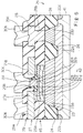
- a bipolar transistor embodying the present invention is fabricated on a lightly doped p-type single crystal silicon substrate 21.
- the lightly doped p-type single crystal silicon substrate 21 ranges 10 ohm-cm to 20 ohm-cm at room temperature, and is oriented to (100) crystal direction.
- Arsenic or antimony is diffused into a part of the lightly doped p-type single crystal silicon substrate 21, and a heavily doped n-type buried layer 22a is formed in the part of the lightly doped p-type single crystal silicon substrate 21.
- boron is doped into the lightly doped p-type single crystal silicon substrate 21, and forms heavily doped p-type channel stopper regions 22b and 22c.
- n-type single crystal silicon layer 23 is epitaxially grown on the lightly doped p-type single crystal silicon substrate 21, the heavily doped n-type buried layer 22a and the heavily doped p-type channel stopper regions 22b and 22c.
- the n-type single crystal silicon layer 23 is doped with phosphorus at 1 x 10 17 cm -3 , and is of the order of 0.4 micron thick.
- a thick field oxide layer 24 protrudes from the surface of the n-type single crystal silicon layer 23 into the lightly doped p-type single crystal silicon substrate 21 and the heavily doped n-type buried layer 22a, and the heavily doped p-type channel stopper regions 22b and 22c are beneath the thick field oxide layer 24.
- the thick field oxide layer 24 is 4000 angstroms thick, and a local oxidation of silicon technology is available for the growth of the thick field oxide layer 24.
- the thick field oxide layer 24 electrically isolates active areas from one another together with the heavily doped p-type channel stopper regions 22b/22c.
- Figure 3 shows one of the active areas assigned to the bipolar transistor.
- a part of the thick field oxide layer 24 reaches the heavily doped n-type buried layer 22a, and separates a single crystal silicon collector region 23a from a collector contact region 23b.
- the collector contact region 23b is heavily doped with phosphorus.
- the n-type single crystal silicon layer 23 and the thick field oxide layer 24 are covered with a silicon oxide layer 25, and the silicon oxide layer 25 is of the order of 1000 angstroms thick.
- a hollow space 25a and a contact hole 25b are formed in the silicon oxide layer 25.
- the hollow space 25a exposes the surface of the single crystal silicon collector region 23a, and the heavily doped n-type collector contact region 23b is exposed to the contact hole 25b.
- the inner surfaces 25c and 25d partially define the hollow space 25a and the contact hole 25b, respectively, and extend in ⁇ 110> direction perpendicular to the paper where figure 3 is drawn.
- silicon foundation 26 The structure below the silicon oxide layer 25 is hereinbelow referred to as "silicon foundation 26", and the lightly doped p-type single crystal silicon substrate 21, the heavily doped n-type buried layer 22a, the heavily doped p-type channel stopper regions 22b/22c, the n-type single crystal silicon layer 23 and the thick field oxide layer 24 form in combination the silicon foundation 26.
- a p-type polysilicon base electrode 27 is provided on the silicon oxide layer 25, and has an over-hang portion 27a.
- the over-hang portion 27a extends over the periphery of the hollow space 25a, and, accordingly, the lower surface of the over-hang portion 27a is exposed to the hollow space 25a.
- the horizontal length of the over-hang portion 27a is greater than the thickness of the silicon oxide layer 25.
- the contact hole 25b is plugged with an n-type polysilicon collector electrode 28, and the n-type polysilicon collector electrode 28 projects over the upper surface of the silicon oxide layer 25.
- the n-type polysilicon collector electrode 28 is held in contact with the n-type collector contact region 23b.
- the p-type polysilicon base electrode 27, the n-type polysilicon collector electrode 28 and the exposed surface of the silicon oxide layer 25 are covered with a silicon nitride layer 29, and contact holes 29a, 29b and 29c are formed in the silicon nitride layer 29.
- the contact hole 29a exposes a part of the p-type polysilicon base electrode 27, and a metallic base electrode 30a in aluminum system is held in contact through the contact hole 29a with the p-type polysilicon base electrode 27.
- the contact hole 29c exposes a part of the n-type polysilicon collector electrode 28, and a metallic collector electrode 30b in the aluminum system is also held through the contact hole 29c with the n-type polysilicon collector electrode 28.
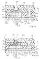
- a base structure 31 is provided on the single crystal silicon collector region 23a, and includes an undoped single crystal silicon germanium layer 31a on the single crystal silicon collector region 23a, a heavily doped p-type single crystal silicon germanium layer 31b laminated on the undoped single crystal silicon germanium layer 31a, a heavily doped p-type single crystal silicon layer 31c on the peripheral area of the heavily doped p-type single crystal silicon germanium layer 31b and a p-type polycrystal laminated structure 31d between the lower surface of the over-hang portion 27a and the heavily doped p-type single crystal silicon layer 31c.
- the p-type poly-crystal laminated structure 31d is partially formed of silicon germanium and partially formed of silicon.
- the undoped single crystal silicon germanium layer 31a is less in dopant concentration than 4 x 10 16 cm -3 , and is deemed to be undoped.
- the undoped single crystal silicon germanium layer 31a is expressed as Si 0.9 Ge 0.1
- the heavily doped p-type single crystal silicon germanium layer 31b has the same composition as the undoped single crystal silicon germanium layer 31a.
- the undoped single crystal silicon germanium layer 31a and the heavily doped p-type single crystal silicon germanium layer 31b are decreased in thickness toward the outer peripheries thereof, and have respective trapezoidal cross sections.
- the heavily doped p-type single crystal silicon layer 31c is increased in thickness toward the outer periphery thereof, and the sloop of the heavily doped p-type single crystal silicon layer 31c is held in contact with the sloop of the heavily doped p-type single crystal silicon germanium layer 31b.
- a heavily doped n-type single crystal silicon emitter region 32a is held in contact with a central area of the heavily doped p-type single crystal silicon germanium layer 31b, and is surrounded by the heavily doped p-type single crystal silicon layer 31c.
- a silicon oxide wall 33 covers the inner surface of the silicon nitride layer 29 defining the contact hole 29b, and the lower surface of the silicon oxide wall 22 is held in contact with the periphery of the heavily doped n-type single crystal silicon emitter region 32a. As a result, a central area of the heavily doped n-type single crystal silicon emitter region 32a is exposed to a hole defined by the silicon oxide wall 33.
- a heavily doped n-type polysilicon emitter electrode 32b is formed in the hole defined by the silicon oxide wall 33, and is held in contact with the heavily doped n-type single crystal silicon emitter region 32a.
- a metallic emitter electrode 30c in the aluminum system is in contact with the heavily doped n-type polysilicon emitter electrode 32b.
- the bipolar transistor shown in figure 3 is fabricated through a process described hereinbelow with reference to figures 4A to 4G.
- the process starts with preparation of the lightly doped p-type single crystal silicon substrate 21 .
- the surface orientation is (100), and the resistivity ranges between 10 ohm-cm and 20 ohm-cm as described hereinbefore.
- the heavily doped n-type buried layer 22a and the heavily doped p-type channel stopper regions 22b and 22c are formed in the surface portions of the lightly doped p-type single crystal silicon substrate 21.
- a silicon dioxide layer (not shown) is thermally grown in or deposited through a chemical vapor deposition on the entire surface portion of the lightly doped p-type single crystal silicon substrate 21 to 5000 angstroms thick, and a photo-resist mask (not shown) is provided on the silicon dioxide layer for the heavily doped n-type buried layer 22a.
- the exposed silicon dioxide layer is firstly etched away through a reactive ion etching by 4000 angstroms thick, and the remaining exposed silicon dioxide is etched away in an etchant in hydrofluoric acid system. Then, the lightly doped p-type single crystal silicon substrate 21 is partially exposed to a hole formed in the silicon dioxide layer, and the photo-resist mask is removed from the structure.
- Arsenic is ion implanted into the exposed portion of the lightly doped p-type single crystal silicon substrate 21 at dose of 5 x 10 15 cm -2 under acceleration energy of 70 keV.
- the implanted arsenic is driven into the lightly doped p-type single crystal silicon substrate 21 through a heat treatment in nitrogen ambience at 1100 degrees centigrade for four hours.
- the heavily doped n-type buried layer 22a is formed in the surface portion of the lightly doped p-type single crystal silicon substrate 21, and is 2 microns in depth.
- the silicon dioxide layer is removed in the etching solution in the hydrofluoric acid system.
- an appropriate photo-resist mask (not shown) is formed through the lithographic techniques for the heavily doped p-type channel stopper regions 22b and 22c, and exposes areas on both sides of the heavily doped n-type buried layer 22a.
- Boron is ion implanted into the exposed areas at dose of 1 x 10 13 cm -2 under acceleration energy of 100 keV, and the implanted boron forms the heavily doped p-type channel stopper regions 22b and 22c.
- the photo-resist mask is stripped off, and a heat treatment is carried out in nitrogen ambience at 1000 degrees centigrade for 30 minutes. As a result, the lightly doped p-type single crystal silicon substrate 21 is cured from the crystal damage due to the ion implantation.
- the n-type single crystal silicon layer 23 is epitaxially grown on the lightly doped p-type single crystal silicon substrate 21 to 0.4 micron thick by using an ordinary silicon epitaxial growing technique, and phosphorus is doped into the n-type single crystal silicon layer 23 at 1 x 10 17 cm -3 .
- the n-type single crystal silicon layer 23 is thermally oxidized, and a silicon oxide layer (not shown) of 500 angstroms thick covers the n-type single crystal silicon layer 23.
- Silicon nitride is deposited over the silicon oxide layer to 1000 angstroms thick by using a low-pressure chemical vapor deposition technique, and a silicon nitride layer (not shown) is laminated on the silicon oxide layer.
- An appropriate photo-resist mask (not shown) is provided on the silicon nitride layer for the thick field oxide layer 24, and the silicon nitride layer, the silicon oxide layer and the n-type single crystal silicon layer 23 are partially etched away by using the anisotropic dry etching. Then, a moat (not shown) is formed through the n-type single crystal silicon layer 23, and the depth of the n-type single crystal silicon layer 23 to be etched away is approximately 2100 angstroms.
- the photo-resist mask is stripped off, and the thick field oxide layer 24 is grown in the moat to 4000 angstroms thick through the oxidation.
- the thick field oxide layer 24 penetrates into the surface portions of the lightly doped p-type single crystal silicon substrate 21.
- the silicon foundation 26 is dipped in hot phosphoric acid, and the silicon nitride layer is removed from the n-type single crystal silicon layer 23.
- the resultant structure is illustrated in figure 4A.
- the silicon oxide layer 25 is thermally grown or deposited through the chemical vapor deposition on the silicon foundation 26 to 1300 angstroms thick.
- An appropriate photo-resist mask (not shown) is provided on the silicon oxide layer 25 for the collector contact hole 25b by using the lithographic techniques, and the exposed silicon oxide layer 25 is partially removed by using a dry etching or a wet etching in hydrofluoric acid solution. Then, the collector contact hole 25b is formed in the silicon oxide layer 25.
- Phosphorus is ion implanted into the exposed n-type single crystal silicon layer 23 at dose of 5 x 10 15 cm -2 under acceleration energy of 70 keV.
- the photo-resist mask for the collector contact hole 25b is stripped off, and a heat treatment in nitrogen ambience at 900 degrees centigrade for 30 minutes cures the n-type single crystal silicon layer 23 from the crystal damages due to the ion-implantation.
- the heavily doped n-type collector contact region 23b is formed below the collector contact hole 25b.
- Natural oxide is removed from the heavily doped n-type collector contact region 23b exposed to the collector contact hole 25b by using the hydrofluoric acid solution, and undoped polysilicon is deposited over the entire surface of the structure through the low-pressure chemical vapor deposition to 2500 angstroms thick.
- an undoped polysilicon layer 27' covers the upper surface of the silicon oxide layer 25, and plugs the collector contact hole 25b.
- the resultant structure is illustrated in figure 4B.
- An appropriate photo-resist mask (not shown) is provided on the undoped polysilicon layer 27' for the heavily doped n-type polysilicon electrode 28, and phosphorus is ion implanted into the exposed undoped polysilicon layer at dose of 5 x 10 15 cm -2 under acceleration energy of 70 keV. After the ion-implantation, the photo-resist mask is stripped off. Thus, the undoped polysilicon layer 27' is partially doped with the n-type dopant impurity.
- An appropriate photo-resist mask (not shown) is provided on the remaining undoped polysilicon layer 27' for the heavily doped p-type polysilicon base electrode 29.
- boron is ion implanted into the exposed undoped polysilicon layer at dose of 5 x 10 15 cm -2 under acceleration energy of 15 keV.
- the heavily doped p-type polysilicon base electrode 29 is formed in the remaining polysilicon layer 27'.
- the photo-resist mask is stripped off.
- An appropriate photo-resist mask (not shown) is provided for the heavily doped p-type polysilicon base electrode 27.
- a dry etching patterns the remaining polysilicon layer 27' into the heavily doped p-type polysilicon base electrode 2, and separates the heavily doped p-type polysilicon base electrode 27 from the heavily doped n-type polysilicon collector electrode 28.
- the resultant structure is illustrated in figure 4C.
- silicon nitride is deposited through a low-pressure chemical vapor deposition to 1500 angstroms thick over the entire surface of the structure, and, accordingly, a silicon nitride layer (not shown) covers the heavily doped p-type polysilicon base electrode 29, the heavily doped n-type polysilicon collector electrode 28 and the exposed surface of the silicon oxide layer 25.
- An appropriate photo-resist mask is provided on the silicon nitride layer, and an anisotropic dry etching removes a part of the silicon nitride layer on the silicon oxide layer 6 in the hole formed in the heavily doped p-type polysilicon base electrode 27 and another exposed surface of the heavily doped p-type polysilicon base electrode 27. The photo-resist mask is stripped off.
- Silicon nitride is deposited over the entire surface of the structure through the low-pressure chemical vapor deposition again, and a silicon nitride layer of 1200 angstroms thick covers the silicon nitride layer on the heavily doped p-type polysilicon base electrode 27 and the exposed surface of the silicon oxide layer 28.
- the silicon nitride layer on the heavily doped p-type polysilicon base electrode 27 increases the thickness.
- the dry etching uniformly removes the silicon nitride until 1200 angstroms, and the silicon nitride layer 29 is completed on the heavily doped p-type polysilicon base electrode 27.
- the inner edge of the heavily doped p-type polysilicon base electrode 27 is covered with the silicon nitride, and the silicon nitride defines the hole 29b. However, the silicon oxide layer 25 is exposed to the hole 29b again. The silicon nitride is also left on the upper and side surfaces of the heavily doped n-type polysilicon collector electrode 28.
- the resultant structure is dipped into hydrofluoric acid solution, and the silicon oxide layer 25 is exposed through the hole 29b to the hydrofluoric acid solution.
- the hydrofluoric acid solution etches the silicon oxide away, and the hollow space sidewardly expands.
- the lower surface of the heavily doped p-type polysilicon base electrode 27 is exposed to the hollow space 25a, and the over-hang portion 27a is completed.
- the width of the exposed lower surface or the distance between the inner edge 25c and the inner edge of the heavily doped p-type polysilicon base electrode 27 is, by way of example, 2000 angstroms.
- the width of the exposed lower surface is equal to or greater than the width of the intrinsic base 31a/31b on the collector 23a, and is equal to or less than the thickness of the heavily doped p-type polysilicon base electrode 27. If the width of the lower surface is greater than the thickness of the polysilicon base electrode 27, the heavily doped p-type polysilicon base electrode dominates the base resistance. On the other hand, if the width of the lower surface is less than the width of the intrinsic base 31a/31b, the intrinsic base 31a/31b dominates the base resistance.
- the undoped single crystal silicon germanium layer 31a and the heavily doped p-type single crystal silicon germanium layer 31b are successively grown on the n-type single crystal silicon collector region 23a by using a selectively growing technique such as, for example, a gas source molecular beam epitaxy, an ultra high vacuum chemical vapor deposition or a low-pressure chemical vapor deposition.
- the selective growing technique grows poly-crystal substance on a poly-crystal layer and single-crystal substance on a single crystal layer, but does not grow the poly-crystal substance and the single-crystal substance on an oxide layer and a nitride layer.
- the p-type poly-crystal silicon germanium layer 31d' is grown from the lower surface of the over-hang portion 27a, but the silicon germanium is not grown on the exposed inner edge 25c of the silicon oxide layer 25 and an exposed surface of the silicon nitride layer 29 as shown in figure 4E.
- the growing conditions are appropriately controlled during the selective growth, and the undoped single crystal silicon germanium layer 31a and the heavily doped p-type single crystal silicon germanium layer 31b have the respective trapezoidal cross section.
- the central portions beneath the hole 29b are thick, and the thicknesses are gradually decreased by increasing the distance from the hole 29b toward the inner edges 25c.
- the trapezoidal cross sections are achieved by a supply rate controlling. Namely, when the selective growth is carried out under a high growing temperature and a small amount of process gas, a substantial amount of the process gas is consumed beneath the hole 29b, and the amount of process gas is gradually decreased from the central portion toward the peripheral portion. This results in the trapezoidal cross sections.
- the undoped single crystal silicon germanium layer 31a and the heavily doped p-type single crystal silicon germanium layer 31b are assumed to be grown through the ultra high vacuum chemical vapor deposition.
- the growing conditions are as follows.
- the substrate temperature is 700 degrees centigrade, and the process gas contains Si 2 H 6 of 3 sccm, GeH 4 of 2 sccm and Cl 2 of 0.03 sccm.
- the undoped single crystal silicon germanium layer 31a is less in dopant concentration than 4 x 10 16 cm -3 , and the central flat portion thereof is about 150 angstroms thick.
- the heavily doped p-type single crystal silicon germanium layer 31b is doped with boron at 7 x 10 18 cm -3 , and the central flat portion thereof is about 450 angstroms thick.
- the thickness of the outer peripheral portions of the undoped/heavily doped p-type silicon germanium single crystal layers 31a and 31b less than a critical thickness of Si 0.9 Ge 0.1 for dislocation.
- the peripheral portions less in thickness than the critical thickness do not allow dislocation due to thermal stress to take place.
- the critical thickness of Si 0.9 Ge 0.1 is of the order of 300 to 400 angstroms.
- the selective growth is continued for the heavily doped p-type single crystal silicon layer 31c.
- the growing conditions are the substrate temperature at 590 degrees centigrade and the process gas containing Si 2 H 6 of 3 sccm and Cl 2 of 0.03 sccm. These growing conditions result in the heavily doped p-type single crystal silicon layer 31c increasing the thickness from the central flat portion toward the outer periphery.
- the heavily doped p-type single crystal silicon layer 31c is doped with boron at 7 x 10 18 cm -3 , and the central flat portion thereof is about 250 angstroms thick.
- the base structure 31 is completed in the hollow space 25a as shown in figure 4F.
- the undoped single crystal silicon germanium layer 31a and the heavily doped p-type single crystal silicon germanium layer 31b form in combination an intrinsic base layer, and the p-type poly-crystal laminated structure 31d and the heavily doped single crystal silicon layer 31c as a whole constitute an extrinsic base layer.
- silicon oxide is deposited over the entire surface of the structure by using the low-pressure chemical vapor deposition, and a silicon oxide layer (not shown) covers the silicon nitride layer 27 and the base structure 31 in the hollow space 25a.
- the anisotropic dry etching removes the silicon oxide on the upper surface of the silicon nitride layer 27 and the base structure 31. however, the side wall 33 is left on the inner vertical surface of the silicon nitride layer 27.
- Polysilicon is deposited over the entire surface of the structure, and arsenic is doped during the deposition of the polysilicon.
- the arsenic-doped polysilicon layer (not shown) is patterned into the heavily doped n-type polysilicon emitter electrode 32b through the anisotropic dry etching without a mask, and the heavily doped n-type polysilicon emitter electrode 32b is 1 x 10 21 cm -3 in dopant concentration and 1700 angstroms in thickness.
- the uniform anisotripic etching or an etch-back technique forms the heavily doped n-type polysilicon emitter electrode 32b in the hole defined by the side wall 33.
- the heavily doped n-type polysilicon layer may be patterned into the heavily doped n-type emitter electrode 32b by using the lithographic techniques.
- Undoped polysilicon deposited by the low-pressure chemical vapor deposition may be ion implanted with n-type dopant impurity instead of the in-situ doping.
- the heavily doped n-type polysilicon emitter electrode 32b is heated so as to diffuse the arsenic into a central portion of the heavily doped p-type silicon layer 31c, and the emitter region 32a is formed as shown in figure 4G.
- the silicon oxide layer 25, the single crystal silicon collector region 23a and the undoped/heavily doped p-type silicon germanium layers 31a and 31b differently expand, and thermal stress takes place in the undoped/heavily doped p-type silicon germanium layers 31a and 31b.
- the thin peripheral portions prevent the undoped/heavily doped p-type silicon germanium layers 31a/31b from dislocation due to the thermal stress.
- an appropriate photo-resist mask (not shown) is provided on the silicon nitride layer 29 for the base contact hole 29a and the collector contact hole 29c, and the exposed portions of the silicon nitride layer 29 are removed so as to expose the heavily doped p-type polysilicon base electrode 27 and the heavily doped n-type polysilicon collector electrode 28 to the base contact hole 29a and the collector contact hole 29c.
- the photo-resist mask is stripped off.
- Conductive alloy such as aluminum containing silicon at 1 percent is sputtered onto the entire surface of the structure, and the sputtering fills the base contact hole 29a, the hole over the emitter electrode 32b and the collector contact hole 29c with the conductive alloy.
- An appropriate photo-resist mask (not shown) is provided on the conductive alloy layer, and the conductive alloy layer is patterned into the metallic base electrode 30a, the metallic emitter electrode 30c and the metallic collector electrode 30b.
- the silicon germanium is grown at relatively high temperature, and the growth at the relatively high temperature decreases the thickness of the silicon germanium layers from the central portion toward the outer periphery.
- the silicon is grown at relatively low temperature, and the growth at the relatively low temperature increases the thickness of the silicon layer from the central portion toward the outer periphery.
- the thickness of the intrinsic base is decreased from the central portion to the outer periphery without deterioration of contact with the extrinsic base, and the thin peripheral portion of the intrinsic base relieves the thick central portion from the thermal stress. Accordingly, the leakage current across the intrinsic base is drastically decreased.
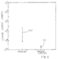
- the present inventor confirmed the reduction of the leakage current.
- the present inventor fabricated the bipolar transistor shown in figure 3 and the prior art bipolar transistor.
- the intrinsic base of the bipolar transistor according to the present invention was equal in germanium content and the boron content to the intrinsic base of the prior art bipolar transistor.
- the central portion of the intrinsic base of the present invention was as thick as the central portion of the intrinsic base of the prior art, the intrinsic base of the present invention was decreased toward the outer periphery, but the intrinsic base of the present invention is constant in thickness between the central portion and the peripheral portion.
- the diffusion for the emitter regions were carried out through a rapid thermal anneal at 1000 degrees centigrade for 10 seconds.
- the base-collector junctions were reversely biased at 5 volts, and the present inventor measured the leakage current for the bipolar transistor according to the present invention and the prior art bipolar transistor.
- the leakage current of each bipolar transistor of the present invention was plotted on line PL1, and the leakage current of the prior art bipolar transistor was varied on line PL2.
- the leakage current of the prior art bipolar transistor ranges from 10 -9 ampere to 10 -6 ampere, and the leakage current of the present invention is of the order of 10 -10 ampere.
- the present inventor confirmed the intrinsic base decreased in thickness toward the periphery is effective against the leakage current.
- bipolar transistors according to the present invention form a semiconductor integrated circuit device, there is only small probability of a defective bipolar transistor due to large leakage current, and the production yield is surely enhanced.
- Another advantage of the bipolar transistor according to the present invention is reduction of the base resistance.
- the base resistance of the bipolar transistor was decreased at 15 percent with respect to the base resistance of the prior art bipolar transistor.
- This advantage is derived from the poly-crystal silicon germanium layer 31d' thinner than the poly-crystal silicon germanium layer of the prior art bipolar transistor. If the germanium content is increased at 10 percent, the diffusion coefficient of boron takes a figure down. In other words, the boron is not widely diffused in the silicon germanium in comparison with the silicon.
- the p-type poly-crystal silicon germanium layer 31d' is grown during the undoped/heavily doped p-type silicon germanium layers 31a/31b, and merely forms a part of the p-type poly-crystal laminated structure 31d. For this reason, the boron is easily diffused from the over-hang portion 27a through the thin poly-crystal silicon germanium layer 31d', and effectively decreases the resistance of the extrinsic base of the bipolar transistor according to the present invention.
- FIG. 6 of the drawings another bipolar transistor embodying the present invention is fabricated on a lightly doped p-type single crystal silicon substrate 41.
- the bipolar transistor shown in figure 6 is similar to the first embodiment except for a base structure 42, and the other regions and layers are labeled with the same references designating corresponding regions and layers of the first embodiment.
- the base structure 42 includes an intrinsic base and an extrinsic base as similar to the first embodiment.
- the intrinsic base is constituted by an undoped single crystal silicon germanium layer 42a and a heavily doped p-type single crystal silicon germanium graded layer 42d.
- the undoped single crystal silicon germanium layer 42a is decreased in thickness from the flat central portion below the hole 29b toward the outer periphery as similar to that of the first embodiment.
- the heavily doped p-type single crystal silicon germanium graded layer 42b decreases the germanium content toward the heavily doped n-type emitter region 32a, and the germanium content is varied from 10 percent to zero.
- the undoped single crystal silicon germanium layer 42a is grown under the similar conditions to the undoped single crystal silicon germanium layer 31a.
- the heavily doped p-type single crystal silicon germanium graded layer 42d is grown under the conditions of growing temperature at 590 degrees centigrade and boron concentration of 7 x 10 18 cm -3 , and the flat central portion is 450 angstroms in thickness.
- the heavily doped p-type silicon germanium graded layer 42b increases the thickess under the over-hang portion 27a, and the thickness of the peripheral portion under the over-hang portion 27a is as thick as 800 angstroms.
- the reason for the thick peripheral portion is Cl 2 added to the process gas. Cl 2 restricts the growth under the hole 29b, and the makes the peripheral portion thicker than the flat central portion.
- the extrinsic base is constituted by the heavily doped p-type single crystal silicon layer 42c and the p-type poly-crystal laminated structure 42d as similar to the first embodiment.
- the process sequence from the extrinsic base to the metallic electrodes 30a to 30c is similar to that of the first embodiment, and description is omitted for avoiding repetition.
- the critical thickness for the dislocation is increased in value by decreasing the germanium content, and only a small amount of dislocation takes place.
- the silicon oxide layer 45 is increased in thickness than the silicon oxide layer 5.
- the total thickness of the selective epitaxially grown layers 42a, 42b and 32a is 850 angstroms, i.e., (150 + 450 + 250) angstroms, and the silicon oxide layer 45 is increased from 1000 angstroms thick to 1400 angstroms thick.
- the total thickness of the epitaxially grown layers 42b and 42c is estimated at 1250 angstroms, i.e., (450 + 250) x (8/4.5) where "450" and "250" are thickness of the heavily doped p-type single crystal silicon germanium graded layer 42b and the thickness of the heavily doped single crystal silicon layer 42c in angstrom and (8/4.5) is indicative of growing ratio of the peripheral portions below the over-hang portion 27a to the central portions below the hole 29b.
- the p-type poly-crystal laminated structure 31d is of the order of 150 angstroms thick.
- the total thickness is 1400 angstroms, and the silicon oxide layer 45 is adjusted to the total thickness.
- the bipolar transistor implementing the second embodiment has the silicon oxide layer 45 thicker than the silicon oxide layer 5, and, accordingly, the parasitic capacitance between the over-hang portion 27a and the collector region 23a is effectively decreased. This results in speed-up.
- the bipolar transistor according to the present invention may form a part of an large scale integration
- field effect transistors may form a semiconductor device together with the bipolar transistors according to the present invention.
- the semiconductor substances for the collector and the base structure and the insulating substance for defining the hollow space are not limited to those of the embodiment.
- the base structure according to the present invention is effective against the dislocation in so far as the lattice constants and/or the thermal expansion coefficients are different between the substances formed in and around the hollow space.
- composition of silicon germanium and the dopant concentrations of the semiconductor layers are not limited to those of the first and second embodiments.
- n-p-n type bipolar transistors are described hereinbefore.
- a p-n-p type bipolar transistor is similarly fabricated on an n-type silicon substrate by exchanging the conductivity types of the semiconductor layers.
Landscapes
- Bipolar Transistors (AREA)
Applications Claiming Priority (2)
| Application Number | Priority Date | Filing Date | Title |
|---|---|---|---|
| JP6217351A JP2679639B2 (ja) | 1994-09-12 | 1994-09-12 | 半導体装置及びその製造方法 |
| JP217351/94 | 1994-09-12 |
Publications (3)
| Publication Number | Publication Date |
|---|---|
| EP0701287A2 EP0701287A2 (en) | 1996-03-13 |
| EP0701287A3 EP0701287A3 (OSRAM) | 1996-03-27 |
| EP0701287B1 true EP0701287B1 (en) | 1999-03-24 |
Family
ID=16702817
Family Applications (1)
| Application Number | Title | Priority Date | Filing Date |
|---|---|---|---|
| EP95114238A Expired - Lifetime EP0701287B1 (en) | 1994-09-12 | 1995-09-11 | Bipolar transistor free from leakage current across thin base region and process of fabrication thereof |
Country Status (5)
| Country | Link |
|---|---|
| US (1) | US5698890A (OSRAM) |
| EP (1) | EP0701287B1 (OSRAM) |
| JP (1) | JP2679639B2 (OSRAM) |
| KR (1) | KR0180325B1 (OSRAM) |
| DE (1) | DE69508506T2 (OSRAM) |
Families Citing this family (29)
| Publication number | Priority date | Publication date | Assignee | Title |
|---|---|---|---|---|
| JP2746225B2 (ja) * | 1995-10-16 | 1998-05-06 | 日本電気株式会社 | 半導体装置及びその製造方法 |
| EP0818829A1 (en) * | 1996-07-12 | 1998-01-14 | Hitachi, Ltd. | Bipolar transistor and method of fabricating it |
| JPH11126781A (ja) * | 1997-10-24 | 1999-05-11 | Nec Corp | 半導体装置及びその製造方法 |
| US6143655A (en) | 1998-02-25 | 2000-11-07 | Micron Technology, Inc. | Methods and structures for silver interconnections in integrated circuits |
| US6121126A (en) | 1998-02-25 | 2000-09-19 | Micron Technologies, Inc. | Methods and structures for metal interconnections in integrated circuits |
| US6492694B2 (en) | 1998-02-27 | 2002-12-10 | Micron Technology, Inc. | Highly conductive composite polysilicon gate for CMOS integrated circuits |
| US6815303B2 (en) * | 1998-04-29 | 2004-11-09 | Micron Technology, Inc. | Bipolar transistors with low-resistance emitter contacts |
| FR2779572B1 (fr) * | 1998-06-05 | 2003-10-17 | St Microelectronics Sa | Transistor bipolaire vertical a faible bruit et procede de fabrication correspondant |
| JP3329762B2 (ja) | 1999-04-27 | 2002-09-30 | 日本電気株式会社 | 半導体装置の製造方法 |
| US6521974B1 (en) * | 1999-10-14 | 2003-02-18 | Hitachi, Ltd. | Bipolar transistor and manufacturing method thereof |
| US6573539B2 (en) * | 2000-01-10 | 2003-06-03 | International Business Machines Corporation | Heterojunction bipolar transistor with silicon-germanium base |
| US6531369B1 (en) * | 2000-03-01 | 2003-03-11 | Applied Micro Circuits Corporation | Heterojunction bipolar transistor (HBT) fabrication using a selectively deposited silicon germanium (SiGe) |
| US6509242B2 (en) * | 2001-01-12 | 2003-01-21 | Agere Systems Inc. | Heterojunction bipolar transistor |
| US6770134B2 (en) * | 2001-05-24 | 2004-08-03 | Applied Materials, Inc. | Method for fabricating waveguides |
| US6905542B2 (en) * | 2001-05-24 | 2005-06-14 | Arkadii V. Samoilov | Waveguides such as SiGeC waveguides and method of fabricating the same |
| WO2002099890A1 (en) * | 2001-06-05 | 2002-12-12 | Sony Corporation | Semiconductor layer and forming method therefor, and semiconductor device and production method therefor |
| US6967144B1 (en) | 2001-06-20 | 2005-11-22 | National Semiconductor Corporation | Low doped base spacer for reduction of emitter-base capacitance in bipolar transistors with selectively grown epitaxial base |
| JP4168615B2 (ja) * | 2001-08-28 | 2008-10-22 | ソニー株式会社 | 半導体装置および半導体装置の製造方法 |
| FR2829288A1 (fr) * | 2001-09-06 | 2003-03-07 | St Microelectronics Sa | Structure de contact sur une region profonde formee dans un substrat semiconducteur |
| DE10164176B4 (de) * | 2001-12-27 | 2007-12-27 | Austriamicrosystems Ag | Bipolartransistor |
| US6867477B2 (en) * | 2002-11-07 | 2005-03-15 | Newport Fab, Llc | High gain bipolar transistor |
| US7038298B2 (en) * | 2003-06-24 | 2006-05-02 | International Business Machines Corporation | High fT and fmax bipolar transistor and method of making same |
| US6888221B1 (en) | 2004-04-14 | 2005-05-03 | International Business Machines Corporation | BICMOS technology on SIMOX wafers |
| EP1878045A2 (en) * | 2005-04-28 | 2008-01-16 | Nxp B.V. | Bipolar transistor and method of fabricating the same |
| US8435873B2 (en) | 2006-06-08 | 2013-05-07 | Texas Instruments Incorporated | Unguarded Schottky barrier diodes with dielectric underetch at silicide interface |
| JP2009043866A (ja) * | 2007-08-08 | 2009-02-26 | Nec Electronics Corp | 半導体装置およびその製造方法 |
| DE102020118776B4 (de) | 2019-10-31 | 2025-11-13 | Taiwan Semiconductor Manufacturing Co., Ltd. | Bipolartransistor (bjt) mit einem dielektrischen mehrschichtbasisfilm |
| US11183587B2 (en) * | 2019-10-31 | 2021-11-23 | Taiwan Semiconductor Manufacturing Company, Ltd. | Bipolar junction transistor (BJT) comprising a multilayer base dielectric film |
| CN111739939B (zh) * | 2020-07-06 | 2024-12-06 | 重庆邮电大学 | 一种高频硅锗异质结双极晶体管及其制造方法 |
Family Cites Families (9)
| Publication number | Priority date | Publication date | Assignee | Title |
|---|---|---|---|---|
| US5296391A (en) * | 1982-03-24 | 1994-03-22 | Nec Corporation | Method of manufacturing a bipolar transistor having thin base region |
| JPH0666318B2 (ja) * | 1985-08-20 | 1994-08-24 | 富士通株式会社 | ヘテロ接合バイポ−ラ半導体装置 |
| JPS63308377A (ja) * | 1987-06-10 | 1988-12-15 | Fujitsu Ltd | バイポ−ラトランジスタの製造方法 |
| JP2522384B2 (ja) * | 1989-03-07 | 1996-08-07 | 日本電気株式会社 | 化合物半導体バイポ―ラトランジスタ |
| US5017990A (en) * | 1989-12-01 | 1991-05-21 | International Business Machines Corporation | Raised base bipolar transistor structure and its method of fabrication |
| JP2705344B2 (ja) * | 1990-04-13 | 1998-01-28 | 日本電気株式会社 | 半導体装置及びその製造方法 |
| JP2855908B2 (ja) * | 1991-09-05 | 1999-02-10 | 日本電気株式会社 | 半導体装置及びその製造方法 |
| US5321301A (en) * | 1992-04-08 | 1994-06-14 | Nec Corporation | Semiconductor device |
| JPH0793315B2 (ja) * | 1992-11-27 | 1995-10-09 | 日本電気株式会社 | 半導体装置およびその製造方法 |
-
1994
- 1994-09-12 JP JP6217351A patent/JP2679639B2/ja not_active Expired - Fee Related
-
1995
- 1995-09-11 EP EP95114238A patent/EP0701287B1/en not_active Expired - Lifetime
- 1995-09-11 DE DE69508506T patent/DE69508506T2/de not_active Expired - Fee Related
- 1995-09-12 US US08/526,893 patent/US5698890A/en not_active Expired - Fee Related
- 1995-09-12 KR KR1019950029729A patent/KR0180325B1/ko not_active Expired - Fee Related
Also Published As
| Publication number | Publication date |
|---|---|
| KR0180325B1 (ko) | 1999-03-20 |
| US5698890A (en) | 1997-12-16 |
| DE69508506T2 (de) | 1999-10-21 |
| EP0701287A3 (OSRAM) | 1996-03-27 |
| DE69508506D1 (de) | 1999-04-29 |
| JP2679639B2 (ja) | 1997-11-19 |
| KR960012555A (ko) | 1996-04-20 |
| JPH0883805A (ja) | 1996-03-26 |
| EP0701287A2 (en) | 1996-03-13 |
Similar Documents
| Publication | Publication Date | Title |
|---|---|---|
| EP0701287B1 (en) | Bipolar transistor free from leakage current across thin base region and process of fabrication thereof | |
| US6436781B2 (en) | High speed and low parasitic capacitance semiconductor device and method for fabricating the same | |
| US5504018A (en) | Process of fabricating bipolar transistor having epitaxially grown base layer without deterioration of transistor characteristics | |
| KR0132769B1 (ko) | 헤테로 바이폴라 트랜지스터와 그 제조 방법 | |
| US6521974B1 (en) | Bipolar transistor and manufacturing method thereof | |
| US5356821A (en) | Method for manufacturing semiconductor integrated circuit device | |
| US6049098A (en) | Bipolar transistor having an emitter region formed of silicon carbide | |
| KR100244812B1 (ko) | 반도체 장치 및 그 제조 방법 | |
| US5798561A (en) | Bipolar transistor with polysilicon base | |
| US4706378A (en) | Method of making vertical bipolar transistor having base above buried nitride dielectric formed by deep implantation | |
| US5523245A (en) | Process for fabricating high-performance facet-free small-sized bipolar transistor | |
| JPH07183310A (ja) | 半導体装置及びその製造方法 | |
| US5723378A (en) | Fabrication method of semiconductor device using epitaxial growth process | |
| EP0052198B1 (en) | Method of manufacturing semiconductor devices using self-alignment techniques | |
| JP2705344B2 (ja) | 半導体装置及びその製造方法 | |
| US5846869A (en) | Method of manufacturing semiconductor integrated circuit device | |
| US5374846A (en) | Bipolar transistor with a particular base and collector regions | |
| JPH10326793A (ja) | 半導体装置の製造方法 | |
| US6211029B1 (en) | Process of fabricating a bipolar transistor having lightly doped epitaxial collector region constant in dopant impurity | |
| EP0045848B1 (en) | Planar semiconductor integrated circuits including improved bipolar transistor structures and method of fabricating such circuits | |
| JP3033155B2 (ja) | 半導体装置の製造方法 | |
| EP0476412B1 (en) | Bipolar transistor and fabrication method thereof | |
| JPH0482180B2 (OSRAM) | ||
| KR100216510B1 (ko) | 트렌치를 이용한 바이폴라 트랜지스터의 컬렉터 형성방법 | |
| JP3254691B2 (ja) | バイポーラトランジスタの製造方法 |
Legal Events
| Date | Code | Title | Description |
|---|---|---|---|
| PUAI | Public reference made under article 153(3) epc to a published international application that has entered the european phase |
Free format text: ORIGINAL CODE: 0009012 |
|
| PUAL | Search report despatched |
Free format text: ORIGINAL CODE: 0009013 |
|
| AK | Designated contracting states |
Kind code of ref document: A2 Designated state(s): DE FR NL |
|
| AK | Designated contracting states |
Kind code of ref document: A3 Designated state(s): DE FR NL |
|
| 17P | Request for examination filed |
Effective date: 19960215 |
|
| GRAG | Despatch of communication of intention to grant |
Free format text: ORIGINAL CODE: EPIDOS AGRA |
|
| 17Q | First examination report despatched |
Effective date: 19980304 |
|
| GRAG | Despatch of communication of intention to grant |
Free format text: ORIGINAL CODE: EPIDOS AGRA |
|
| GRAG | Despatch of communication of intention to grant |
Free format text: ORIGINAL CODE: EPIDOS AGRA |
|
| GRAH | Despatch of communication of intention to grant a patent |
Free format text: ORIGINAL CODE: EPIDOS IGRA |
|
| GRAH | Despatch of communication of intention to grant a patent |
Free format text: ORIGINAL CODE: EPIDOS IGRA |
|
| GRAA | (expected) grant |
Free format text: ORIGINAL CODE: 0009210 |
|
| AK | Designated contracting states |
Kind code of ref document: B1 Designated state(s): DE FR NL |
|
| REF | Corresponds to: |
Ref document number: 69508506 Country of ref document: DE Date of ref document: 19990429 |
|
| ET | Fr: translation filed | ||
| PLBE | No opposition filed within time limit |
Free format text: ORIGINAL CODE: 0009261 |
|
| STAA | Information on the status of an ep patent application or granted ep patent |
Free format text: STATUS: NO OPPOSITION FILED WITHIN TIME LIMIT |
|
| 26N | No opposition filed | ||
| NLS | Nl: assignments of ep-patents |
Owner name: NEC ELECTRONICS CORPORATION |
|
| PGFP | Annual fee paid to national office [announced via postgrant information from national office to epo] |
Ref country code: FR Payment date: 20030909 Year of fee payment: 9 |
|
| PGFP | Annual fee paid to national office [announced via postgrant information from national office to epo] |
Ref country code: DE Payment date: 20030918 Year of fee payment: 9 |
|
| PGFP | Annual fee paid to national office [announced via postgrant information from national office to epo] |
Ref country code: NL Payment date: 20030922 Year of fee payment: 9 |
|
| REG | Reference to a national code |
Ref country code: FR Ref legal event code: TP |
|
| PG25 | Lapsed in a contracting state [announced via postgrant information from national office to epo] |
Ref country code: NL Free format text: LAPSE BECAUSE OF NON-PAYMENT OF DUE FEES Effective date: 20050401 Ref country code: DE Free format text: LAPSE BECAUSE OF NON-PAYMENT OF DUE FEES Effective date: 20050401 |
|
| PG25 | Lapsed in a contracting state [announced via postgrant information from national office to epo] |
Ref country code: FR Free format text: LAPSE BECAUSE OF NON-PAYMENT OF DUE FEES Effective date: 20050531 |
|
| NLV4 | Nl: lapsed or anulled due to non-payment of the annual fee |
Effective date: 20050401 |
|
| REG | Reference to a national code |
Ref country code: FR Ref legal event code: ST |