EP0701008A2 - Epitaxie zur Züchtung von Verbindunghalbleitern und InP Substraten für das Epitaxiezüchten - Google Patents
Epitaxie zur Züchtung von Verbindunghalbleitern und InP Substraten für das Epitaxiezüchten Download PDFInfo
- Publication number
- EP0701008A2 EP0701008A2 EP95306232A EP95306232A EP0701008A2 EP 0701008 A2 EP0701008 A2 EP 0701008A2 EP 95306232 A EP95306232 A EP 95306232A EP 95306232 A EP95306232 A EP 95306232A EP 0701008 A2 EP0701008 A2 EP 0701008A2
- Authority
- EP
- European Patent Office
- Prior art keywords
- hillocks
- substrate
- angle
- dislocations
- inp
- Prior art date
- Legal status (The legal status is an assumption and is not a legal conclusion. Google has not performed a legal analysis and makes no representation as to the accuracy of the status listed.)
- Granted
Links
Images

Classifications
-
- C—CHEMISTRY; METALLURGY
- C30—CRYSTAL GROWTH
- C30B—SINGLE-CRYSTAL GROWTH; UNIDIRECTIONAL SOLIDIFICATION OF EUTECTIC MATERIAL OR UNIDIRECTIONAL DEMIXING OF EUTECTOID MATERIAL; REFINING BY ZONE-MELTING OF MATERIAL; PRODUCTION OF A HOMOGENEOUS POLYCRYSTALLINE MATERIAL WITH DEFINED STRUCTURE; SINGLE CRYSTALS OR HOMOGENEOUS POLYCRYSTALLINE MATERIAL WITH DEFINED STRUCTURE; AFTER-TREATMENT OF SINGLE CRYSTALS OR A HOMOGENEOUS POLYCRYSTALLINE MATERIAL WITH DEFINED STRUCTURE; APPARATUS THEREFOR
- C30B23/00—Single-crystal growth by condensing evaporated or sublimed materials
- C30B23/02—Epitaxial-layer growth
-
- C—CHEMISTRY; METALLURGY
- C30—CRYSTAL GROWTH
- C30B—SINGLE-CRYSTAL GROWTH; UNIDIRECTIONAL SOLIDIFICATION OF EUTECTIC MATERIAL OR UNIDIRECTIONAL DEMIXING OF EUTECTOID MATERIAL; REFINING BY ZONE-MELTING OF MATERIAL; PRODUCTION OF A HOMOGENEOUS POLYCRYSTALLINE MATERIAL WITH DEFINED STRUCTURE; SINGLE CRYSTALS OR HOMOGENEOUS POLYCRYSTALLINE MATERIAL WITH DEFINED STRUCTURE; AFTER-TREATMENT OF SINGLE CRYSTALS OR A HOMOGENEOUS POLYCRYSTALLINE MATERIAL WITH DEFINED STRUCTURE; APPARATUS THEREFOR
- C30B25/00—Single-crystal growth by chemical reaction of reactive gases, e.g. chemical vapour-deposition growth
- C30B25/02—Epitaxial-layer growth
-
- C—CHEMISTRY; METALLURGY
- C30—CRYSTAL GROWTH
- C30B—SINGLE-CRYSTAL GROWTH; UNIDIRECTIONAL SOLIDIFICATION OF EUTECTIC MATERIAL OR UNIDIRECTIONAL DEMIXING OF EUTECTOID MATERIAL; REFINING BY ZONE-MELTING OF MATERIAL; PRODUCTION OF A HOMOGENEOUS POLYCRYSTALLINE MATERIAL WITH DEFINED STRUCTURE; SINGLE CRYSTALS OR HOMOGENEOUS POLYCRYSTALLINE MATERIAL WITH DEFINED STRUCTURE; AFTER-TREATMENT OF SINGLE CRYSTALS OR A HOMOGENEOUS POLYCRYSTALLINE MATERIAL WITH DEFINED STRUCTURE; APPARATUS THEREFOR
- C30B29/00—Single crystals or homogeneous polycrystalline material with defined structure characterised by the material or by their shape
- C30B29/10—Inorganic compounds or compositions
- C30B29/40—AIIIBV compounds wherein A is B, Al, Ga, In or Tl and B is N, P, As, Sb or Bi
-
- Y—GENERAL TAGGING OF NEW TECHNOLOGICAL DEVELOPMENTS; GENERAL TAGGING OF CROSS-SECTIONAL TECHNOLOGIES SPANNING OVER SEVERAL SECTIONS OF THE IPC; TECHNICAL SUBJECTS COVERED BY FORMER USPC CROSS-REFERENCE ART COLLECTIONS [XRACs] AND DIGESTS
- Y10—TECHNICAL SUBJECTS COVERED BY FORMER USPC
- Y10S—TECHNICAL SUBJECTS COVERED BY FORMER USPC CROSS-REFERENCE ART COLLECTIONS [XRACs] AND DIGESTS
- Y10S117/00—Single-crystal, oriented-crystal, and epitaxy growth processes; non-coating apparatus therefor
- Y10S117/901—Levitation, reduced gravity, microgravity, space
- Y10S117/902—Specified orientation, shape, crystallography, or size of seed or substrate
Definitions
- This invention relates to an epitaxial method for suppressing the occurrence of hillocks which are likely to appear on a thin film of a compound semiconductor epitaxially grown on a compound semiconductor substrate in vapor phase.
- the compound semiconductor substrate means a GaAs substrate, an InP substrate and so forth.
- Vapor phase epitaxy is an influential method of growing a compound semiconductor film of either the same component as the substrate or the components different from the substrate material.
- the vapor phase epitaxy includes MOCVD (Metal-Organic Chemical Vapor Deposition), MBE (Molecular Beam Epitaxy), Chloride CVD or Halide CVD. This invention is capable of being applied to all of the vapor phase epitaxy methods.
- Japanese Patent Laying Open No.2-239188 (239188/'90) paid attention to the problem of surface defects called "growth pyramid” or "faceted defects” which arose in the vapor phase epitaxy of compound semiconductors.
- This prior application described that the "off-angle" method had been adopted to suppress the occurrence of the surface defects.
- the off-angle method is a method of growing films epitaxially on a wafer which has an orientation of the surface inclining at 1° to 7° to a (100) plane.
- Off-angled wafers cannot be adopted for making special devices, for example, laser diodes which require forming gratings on the surface waveguides.
- the grating having regularly spaced grooves demands a just-(100) wafer as a substrate.
- the just-(100) wafer means here a wafer having a surface which correctly corresponds to a (100) plane.
- An off-angled (100) wafer indicates a wafer having a surface which inclines slightly to a (100) plane. If the inclination angle is ⁇ , the wafer is designated as a (100) ⁇ ⁇ .
- Japanese Patent Laying Open No.2-239188 proposed an improvement of vapor phase epitaxy including the processes of preparing an off-angle wafer with a slanting-angle between 0.1° and 0.5° to a (100) plane, maintaining the substrate wafer at a temperature between 600°C and 700°C, and growing semiconductor films on the heated, off-angled substrate in vapor phase.
- Japanese Patent Laying Open No.5-301795 (301795/93) proposed a method of reducing droplet-defects appearing on the surface of a substrate in an epitaxial growth of compound semiconductors in vapor phase.
- the prior art suggested an inequality 0.011V 1.5 + 6.21 ⁇ 100T -7.5 ⁇ ⁇ ⁇ 0.20 where ⁇ is the off angle of the wafer from a (100) plane, V is the speed of the epitaxial growth and T is the temperature of the substrate.
- the application mentioned that the defects could be decreased by growing the compound semiconductor films on the wafers which satisfied the inequality. Faster growth demands a higher substrate temperature. Lower growing speed requires a reduction of the substrate temperature to the contrary. This is the meaning of the inequality. It is, however, still unclear why the speed V and temperature T are accompanied with the order of magnitude of 1.5 and -7.5 respectively.
- Japanese Patent Laying Open No.64-32686 (32686/'89) produced avalanche photodiodes by the halogen transport CVD method.
- the application discussed the problems of both an occurrence of a lot of hillocks and a big fluctuation of film thickness of the avalanche layer, when InP wafers having a small off-angle less than ⁇ 0.1° from a (100) plane were adopted as substrates.
- this prior art suggested an epitaxial growth having the processes of preparing off-angle InP wafers inclining at 0.2 degree to 0.5 degree to a (100) plane, and forming epitaxially a light absorption layer and an avalanche layer of the off-angle substrate wafer. They said that the occurrence of hillocks was suppressed by the off-angle substrate.
- Japanese Patent Laying Open No.64-22072 (22072/'89) pointed out the problems of the dispersion of the thicknesses of a window layer and a buffer layer, and of the fluctuation of the depth of pn-junctions, when InP type photodiodes were produced on just-(100) InP wafers by the halogen transport vapor phase epitaxy.
- the prior art suggested a use of an off-angled InP with an off-angle between 0.2 and 0.5 on which a buffer layer and a light absorption layer were deposited. They mentioned that the contrivance succeeded in reducing the fluctuation of the film thicknesses and in enhancing the yield of the products.
- Japanese Patent Laying Open No.64-15914 described the problem of the difficulty of controlling the film thickness due to the occurrence of hillocks, when InP photodiodes were produced by growing epitaxially InGaAsP films and so forth on a just-(100) InP wafer by halogen transport CVD method. They reported that the uniformity of the film thickness was improved by growing multi-layered InGaAsP thin films on an off-angle InP wafer inclining at an angle between 0.2 degree and 0.5 degree to a (100) plane.
- Japanese Patent Laying Open No.1-270599 (270599/'89) alluded the problems of the weak photoluminescence (PL) of a double-hetero structure produced on a just-(100) InP wafer by an MBE method and of the high threshold current of the laser diodes further made on the same double-hetero structure.
- the application suggested a method of fabricating the double-hetero structure by the MBE method on an off-angle InP wafer having a surface slanting at 0.5 degree to 2 degrees to a (111) plane.
- This prior art used a (111) wafer instead of a (100) wafer.
- Japanese Patent Publication No.4-73610 (73610/'92) proposed an epitaxial growth of compound semiconductor films on an off-angle GaAs wafer slanting at 0.1 degree to 1 degree to a (111)B plane for making quantum-well laser diodes or high speed FETs based on the two-dimensional electron gas.
- the inventors told that the inclination of a GaAs wafer ranging from 0.1 degree to 1 degree made the epitaxial films mirror-smooth and enhanced the photoluminescence. They judged the off-angle (111) GaAs wafer was superior to the (001) GaAs wafer.
- Japanese Patent Laying Open No.62-88318 (88318/'87) proposed an epitaxial growth of thin compound semiconductor films on an off-angle (111) GaAs wafer slanting at an angle between 0.1° and 1° to a (111)B plane. They alleged that the thin films deposited on the off-angle (111)B GaAs wafer exhibited stronger photoluminescence than the thin film made on a (001) GaAs wafer.
- Japanese Patent Laying Open No.3-16993 (16993/'91) pointed out the problem of the ruggedness of thin films epitaxially grown on a just-(100) GaAs wafer in vapor phase.
- the ruggedness was induced by the striped morphology called "cross-hatching". They said that the cross-hatchings were reduced by adopting an off-angle wafer slanting at an angle between 0.5 degree and 10 degrees to a (100) plane.
- Japanese Patent Laying Open No.2-288223 (288223/'90) pointed out the problem of the occurrence of rice-grain defects appearing on surfaces of HEMTs (High Electron Mobility Transistor) which were made by growing AlGaAs films on (100) GaAs wafers. They said the rice-grain defects were caused by the inclination of the (100) GaAs wafer to a (100) plane. They alleged that the deviation of the orientation of the (100) wafer should be less than 0.15 degree, preferably less than 0.05 degree in order to prevent the rice-grain defects from arising on the surfaces. This opinion contradicts to the prior art which have been explained till now.
- Japanese Patent Laying Open No.1-128423 (128423/'89) disclosed the employment of an off-angled GaAs wafer slanting at an angle of 0.5 degree to 10 degrees to a (100) plane in order to avoid the ruggedness of the film surfaces brought about by growing a thin films including aluminum on a GaAs wafer either by an MBE method or an MO-MBE method.
- the Inventors of the present invention were aware of a big difference of the density of hillocks appearing on the different films which have been grown on the substrates having the same off-angle. Some films indicate a low density of hillocks but other films exhibit a high density of hillocks, even if the films have been deposited on the substrate wafers having the same off-angle. Almost all of the prior art mentioned till now defined optimum ranges of the off-angles ⁇ from a (100) plane, and explained the density of hillocks would be reduced as a function of the off-angle ⁇ of the substrate wafers. Thus they asserted the ruggedness of the epitaxial wafer should be decreased uniformly in accordance with an increase of the off-angle ⁇ .
- the present Inventors dissent from the prevalent opinion.
- Even the substrates having the same off-angle deviating from the same principal plane make epitaxial films showing very different states of hillocks.
- the inclination angle of the substrate from the principal plane is not a unique parameter which exclusively rules the occurrence of hillocks. Otherwise, hillocks appear or do not appear by some reason other than the off-angle of the substrate or the films.
- the appearance of hillocks is contingent on a certain fact other than the inclination of the film surface to the principal plane.
- Some substrate with a small off-angle (inclination angle) has a small density of hillocks in the films grown on the substrate.
- Other substrate with a big off-angle has a big density of hillocks in the films deposited on the substrate. What does cause such a reverse relation between the off-angle and the hillock density? There should be a hidden parameter of determining the occurrence of hillocks.
- One purpose of the present invention is to clarify the reason why the hillocks are induced on the compound semiconductor films grown on an InP substrate.
- Another purpose of the present invention is to provide an vapor phase epitaxy of compound semiconductor in which the off-angle is pertinently determined for suppressing the generation of hillocks.
- a further purpose of the present invention is to provide an epitaxial InP wafer without hillocks.
- a still further purpose of the present invention is to provide an InP wafer which is immune from hillocks when epitaxial films are grown on it.
- This invention pays attention to the defects on the substrate itself.
- the Inventors have discovered that the density of the hillocks of the film is contingent on the defect density of the substrate itself.
- the hidden parameter which determines the occurrence of the hillocks turns out to be the density of the inherent defects on the substrate.
- Further two elements which determine the density of the hillocks on the film are the inclination angle of the substrate and the density of the inherent defects of the substrate. The Inventors have discovered the fact for the first time.
- this invention changes the inclination angle (off-angle) of the substrate as a function of the density of the defects on the substrate for preventing hillocks from originating on the film grown on the substrate.
- a smaller off-angle of the substrate is allowable.
- a wafer of a bigger off-angle shall be chosen for the substrate.
- the minimum off-angle of a wafer can be determined as a function of the defect density on the substrate for hindering hillocks from arising.
- the Inventors have found the following properties controlling the epitaxy of an InP film on an InP substrate wafer.
- the minimum inclination angle ⁇ is contingent upon the density of defects (EPD) on the substrate.
- EPD density of defects
- the defects sometimes disperse irregularly on a wafer and a microscopic defect density D varies locally on the wafer.
- the expression of the parameters D and ⁇ with three digits may be less significant.
- the inequality is reduced to ⁇ ⁇ 1x10 ⁇ 3D 1 ⁇ 2 .
- the Inventors have noticed the relation between the defects of the substrate and the occurrence of the hillocks for the first time. Namely, the bigger the density of the defects is, the higher the probability of the occurrence of the hillocks is. The fewer defects the substrate has, the lower the frequency of the occurrence of the hillocks rises.
- the off-angle ⁇ of the wafers from (100) plane is first determined and the ingot is cut into wafers in parallel with a plane with the determined off-angle.
- the minimum inclination angle ⁇ min depends on the defect density of the substrate. The dependence is clearly described by the inequality ⁇ ⁇ 1.26 ⁇ 10 ⁇ 3D 1 ⁇ 2 (more roughly ⁇ ⁇ 1 ⁇ 10 ⁇ 3D 1 ⁇ 2 ).
- a small density of defects on the substrate allows a small inclination angle ⁇ for preventing the hillocks from originating.
- the suppression of the hillocks requires a large inclination angle ⁇ for the wafers with lots of defects.
- the optimum off-angle ⁇ depends on the defect density on the wafers from the standpoint of eliminating the hillocks.
- An ingot is sliced into a plurality of as-cut wafers.
- the as-cut wafers are etched and polished into mirror-wafers with mirror-smooth surfaces.
- the defects are counted by etching the mirror-wafers with a special etchant enabling dislocations to appear on the surfaces.
- the defect density cannot be reckoned before being cut into wafers. Thus slicing an ingot precedes counting defects.
- An approximate density of defects can be measured by cutting a part of an ingot, obtaining a small sample wafer, etching the sample, and counting the dislocations appearing on the sample wafer after etching.
- the inclination angle can be determined by the approximate defect density calculated from the sample wafer.
- the ingot can be sliced at the off-angle determined by the defect density measured for the sample wafer.
- the defect density fluctuates in the axial direction in the ingot and the defect density of each wafer will be different from the density of the sample wafer.
- the average density of defects can be surmised by the value of the sample wafer.
- This invention points out a strong correlation between the defects (dislocations) on the substrate and the generation of the hillocks for the first time.
- the defects on the substrate have been deemed to have no relation to the hillocks on the film.
- the inclination angle (off-angle) can be small enough for suppressing the hillocks, if the substrate has a small density of defects.
- the wafer with a large density of defects requires a large off-angle for the substrate in order to annihilate the hillocks.
- This invention proposes a clear criterion for the off-angle ⁇ as a function of the defect density D to make a smooth film on an InP wafer.
- This invention enables an operator to design a correct off-angle in slicing an InP single crystal ingot into a plurality of as-cut wafers.
- the operator can slice an InP ingot into wafers which are immune from the origination of hillocks by the processes of cutting a small part of the ingot, obtaining a sample wafer, etching the sample wafer by some etchant, measuring the EPD on the sample wafer, determining an optimum off-angle, cutting the ingot at the determined off-angle.
- the fabrication of devices, i.e. laser diodes requires the wafers which have an orientation with the least deviation from a (100) plane. Thus the operator will be able to cut the ingot at the best angle which is the smallest off-angle in the solutions of the inequality.
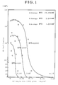
- Fig. 1 is a graph showing the relation between the off-angle ⁇ of an InP substrate and the density of hillocks appearing on the film with a parameter of the defect density of the substrate, when an assembly of films InP/InGaAs/InP is grown epitaxially on the InP substrate.
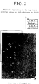
- Fig.2 is a Nomarski microscope photograph on the uppermost InP film epitaxially grown on the InP substrate in the same experiment as in Fig.l.
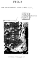
- Fig.3 is a Nomarski microscope photograph of the Hüber-etched substrate revealed by eliminating the films which were grown on the substrate.
- Fig.4 is a schematic view of the band structure showing the energy state on an atom in a trap level.
- Fig.5 is a perspective view of terraces for explaining the behavior of an atom whether the atom goes into a trap or to the step of the terrace, when an atom falls on the terrace.
- a set of thin films InP/InGaAs/InP was epitaxially grown on single crystal InP wafers which incline at a certain off-angle ⁇ to a (100) plane by the OMVPE (Organometallic Vapor Phase Epitaxy) method.
- the inclination angles of the wafers range from 0° to 0.2° .
- the substrate was heated at 873K.
- the speed of the growth was 1.0 ⁇ m/hr.
- the epitaxial wafers were cooled and investigated.
- the number of the hillocks appearing on the uppermost InP film was counted by the observation through a microscope.
- the relation between the hillocks on the film and the defects on the substrate was examined.
- the wafers were classified into three degrees of defects.
- First kind of wafers has an average defect density (EPD) of 25000 cm ⁇ .
- Second kind of wafers has a smaller average defect density of 3000 cm ⁇ .
- Third kind of wafers has a far smaller average defect density of 1000 cm ⁇ .
- Fig. 1 shows the relations between the off-angle of the wafers to a (100) plane and the hillock density on the top film with a parameter of the average defect density on the substrate.
- Blank triangles denote the results on the substrate having an average EPD of 1000 cm ⁇ .
- Blank rounds indicate the results on the substrate of an average EPD of 3000 cm ⁇ .
- Blank squares show the results on the substrate of the average EPD of 25000 cm ⁇ .
- An increase of the inclination angle ⁇ decreases the hillock density drastically.
- a rise of the inclination angle reduces the hillock density.
- Fig.2 is a Nomarski microscope photograph of the top film of a set of films InP/InGaAs/InP epitaxially grown on a Fe-doped just (100) InP wafer by the OMVPE (Organometallic Vapor Phase Epitaxy).
- OMVPE Organic Vapor Phase Epitaxy
- the epitaxial wafer has a multilayered structure of InP/InGaAs/InP/InP(substrate).
- the layers are denoted at the upper right of Fig.2.
- the magnification is approximately 100.
- the arrow shows the object surface of the observation.
- Elliptical defects appear on the top InP film. These defects are called hillocks.
- FIG.3 is a Nomarski microscope photograph of the Huber-etched surface of the substrate with a magnification of approximately 100. The arrow shows the object surface of the observation.
- a hillock is generated by transcribing a dislocation on a just (100) wafer.
- the defects on the substrate generate the hillocks on the film. Few hillocks occur on the region without defects.
- the inclination angle of the substrate from a (100) plane conceals some of the dislocations on the substrate. What prevents the film from transcribing the defects is the inclination angle (off-angle) ⁇ .
- a film is grown on a substrate by the OMVPE method.
- the atoms which arrive at a spot on the surface of the substrate are either captured at the same place into the lattice structure or displaced to another spot of lower potential and assembled into the lattice structure.
- Fig.4 shows a potential curve for explaining the displacement of the supplied atoms.
- E denotes the potential energy of the trap. If the potential E is bigger than the thermal energy kT of the atom, the probability that the atom escapes from the trap is low enough. Thus the atoms stop in the trap and form a part of lattice structure.
- the surface of the substrate forms a plurality of parallel steps.
- the planes parallel with a (100) plane are now called “terrace”.
- the vertical parts are called "edges".
- the edges of the steps are the singular points for the crystal structure.
- the potential energy has the lowest at the singular points.
- Dislocations are defects of the periodic crystal structure.
- the dislocations have a low potential energy for atoms. Thus the dislocations can also trap atoms.
- "a” denotes the lattice constant.
- the terrace has a (100) plane.
- the height of the edge is "a”, because the edge must be a unit of lattice structure.
- the edges are an assembly of parallel lines.
- the width of the terrace is denoted by "W”.
- the length of the crystal is designated by "S”.
- the area of the substrate is SW.
- the flat parts have a higher potential and the edges have a lower potential.
- the terraces scarcely capture atoms because of the higher potential. Then most of the atoms will be captured either by dislocations or by the edges.
- Fig.2 and Fig.3 suggest that the hillocks are transcriptions of the dislocations.
- the hillocks should be made by the successive deposition of atoms on the dislocations. Namely, an abnormal growth on the dislocations makes hillocks.
- the atoms which are trapped at the edges of the steps form a part of an epitaxial film.
- the terrace advances by a volume of an atom. If many atoms align at the edges, the terrace grows forward step by step.
- the number of the terraces or the edges is also small.
- the atoms supplied on the surface have a poor chance of being captured by the step edges. Almost all of the falling atoms will be caught by the dislocations whose number is independent of the inclination ⁇ . The atoms will form big hillocks on the dislocations. Therefore a small ⁇ induces a high density of the hillocks.
- the normal growth on the edges prevails in a big inclination ⁇ .
- the influential normal growth suppresses the abnormal growth, i.e. the origination of hillocks.
- the mean distance of the paths along which the supplied atoms travel from the falling points to the nearest neighboring dislocations can be estimated by D -1 ⁇ 2 which is an inverse of the root of the dislocation density D.
- the mean distance of the paths along which the supplied atoms travel from the falling points to the nearest neighboring edges of the steps can be estimated by a/ ⁇ which is a length of a terrace.
- Atoms replenished from the vapor phase will be captured by the nearer singular points (edges or dislocations). When e is small enough, the atoms are assembled at the dislocations. A plenty of hillocks are generated from the dislocations as seeds. When ⁇ is big, the atoms gather on the edges, which facilitates the normal growth of the film. Since few atoms are accumulated on the dislocations, few hillocks arise.
- the balance between the attraction force from the dislocations and the attraction force from the edges determines whether the supplied atoms are pulled by the dislocations or by the edges.
- R indicates the number of the atoms positioned on the terraces.
- N is the number of the atoms on the dislocations.
- F denotes the number of the atoms which are supplied to the substrate or the film in a unit time.
- ⁇ is the probability of the atoms for transferring from the terrace to the edges in a unit time.
- ⁇ is the probability of the atoms for being solidified at the edges.
- ⁇ means the probability of the atoms for moving from the terrace to the dislocations in a unit time.
- ⁇ is the probability of the atoms of being solidified at the dislocations in a unit time.
- F is the speed of the gas supply. Then F can be deemed a constant value.
- the probability ⁇ of the atoms for being solidified on the edges is contingent upon the temperature and the difference of potential between the edges and the terraces. But ⁇ is independent of the number of the edges.
- the discovery of the Inventors is that the atoms growing on the dislocations form the hillocks.
- the number of the atoms forming the hillocks is ⁇ tF.
- the solidification of ⁇ tF atoms at the edges of the steps corresponds to the normal growth of an epitaxial film.
- ⁇ tF In order to make a thin film immune from the hillocks, ⁇ tF must be far bigger than ⁇ tF. Namely, a should be still bigger than ⁇ for the fabrication of non-hillock films.
- the condition is simply expressed by h ⁇ >> kD 1 ⁇ 2 .
- the condition of suppressing the occurrence of hillocks imposes a condition on ⁇ as ⁇ >> (k/h)D 1 ⁇ 2 .
- the prevention of hillocks demands the off-angle ⁇ to be bigger than a value which is in proportion to the square root D 1 ⁇ 2 of the dislocation density D. This consideration coincides with the actual result.
- the proportional constant can be determined by the previous experiments.
- the condition is determined to be ⁇ ⁇ 1 ⁇ 10 ⁇ 3D 1 ⁇ 2 . Otherwise, ⁇ ⁇ (D/106) 1 ⁇ 2 .
- the lattice constant a is assumed to be 0.5 nm and the off-angle ⁇ from a (100) plane is also assumed to be 0.1°. Then the width of a terrace is 300 nm. By the way, the dislocation density is assumed to be 25000 cm ⁇ . In this case, the average distance between neighboring dislocations is about 60 ⁇ m.
- the average distance between the nearest neighboring dislocations is about 200 times as long as the length of the terraces.
- An atom which has fallen at a spot in the middle of neighboring dislocations must climb up or down on about 100 steps of terraces till it reaches the nearest dislocation.
- the number of dislocations is too small in comparison with the number of the terraces.
- Fig.2 and Fig.3 indicate that a dislocation has a diameter of about 50 ⁇ m. If the terraces have periodic lengths of a period of 0.3 ⁇ m, one dislocation pervades more than 100 steps of the terraces. A dislocation has an influence on the potential energy of a wide range of the terraces.
- ⁇ R is now interpreted not as the atoms which are absorbed in the edges but as the height of the terraces. This interpretation is reasonable, because the height of the terraces is in proportion to the number of the atoms piling on the edges.
- ⁇ N is interpreted as the height of the hillocks. ⁇ N has been the number of the atoms accumulated in the dislocations in the previous explanation. The height of the hillocks is obtained by dividing the number of the atoms adsorbed in the dislocations by the area of the dislocations. Since the differential equations are linear about the variables R and N, the equations hold for the variables which are obtained by multiplying R and N by a multiplier.
- the dislocations are far large odd-looking structures.
- the atoms which have once fallen on the dislocations may return back on the terraces.
- " ⁇ " denotes the probability of the return of the atoms from the dislocations to the terraces.
- some atoms move from the terraces to the dislocations.
- the solutions include time-dependent parts and constant parts.
- the time-dependent parts rapidly diminish.
- ⁇ is positive, because the replacement rate ⁇ from the dislocations to the terraces is far smaller than the solidification rate ⁇ at the dislocations, and because the replacement rate ⁇ from the terraces to the dislocations is far smaller than the solidification rate ⁇ at the edges.
Landscapes
- Chemical & Material Sciences (AREA)
- Engineering & Computer Science (AREA)
- Crystallography & Structural Chemistry (AREA)
- Materials Engineering (AREA)
- Metallurgy (AREA)
- Organic Chemistry (AREA)
- Inorganic Chemistry (AREA)
- Chemical Kinetics & Catalysis (AREA)
- General Chemical & Material Sciences (AREA)
- Crystals, And After-Treatments Of Crystals (AREA)
- Recrystallisation Techniques (AREA)
Applications Claiming Priority (2)
| Application Number | Priority Date | Filing Date | Title |
|---|---|---|---|
| JP06240680A JP3129112B2 (ja) | 1994-09-08 | 1994-09-08 | 化合物半導体エピタキシャル成長方法とそのためのInP基板 |
| JP240680/94 | 1994-09-08 |
Publications (3)
| Publication Number | Publication Date |
|---|---|
| EP0701008A2 true EP0701008A2 (de) | 1996-03-13 |
| EP0701008A3 EP0701008A3 (de) | 1996-06-26 |
| EP0701008B1 EP0701008B1 (de) | 1998-01-14 |
Family
ID=17063117
Family Applications (1)
| Application Number | Title | Priority Date | Filing Date |
|---|---|---|---|
| EP95306232A Expired - Lifetime EP0701008B1 (de) | 1994-09-08 | 1995-09-06 | Epitaxie zur Züchtung von Verbindunghalbleitern und InP Substraten für das Epitaxiezüchten |
Country Status (4)
| Country | Link |
|---|---|
| US (1) | US5647917A (de) |
| EP (1) | EP0701008B1 (de) |
| JP (1) | JP3129112B2 (de) |
| DE (1) | DE69501444T2 (de) |
Cited By (4)
| Publication number | Priority date | Publication date | Assignee | Title |
|---|---|---|---|---|
| WO2002029138A2 (en) * | 2000-09-29 | 2002-04-11 | Showa Denko K.K. | Inp single crystal substrate |
| EP1569269A1 (de) * | 2002-12-03 | 2005-08-31 | Nikko Materials Company, Limited | Epitaxialwachstumsverfahren und substrat für epitaxialwachstum |
| EP1743961A1 (de) * | 2004-03-19 | 2007-01-17 | Nippon Mining & Metals Co., Ltd. | Verbindungshalbleitersubstrat |
| EP1988194A1 (de) * | 2006-02-02 | 2008-11-05 | Nippon Mining & Metals Co., Ltd. | Substrat zum aufwachsenlassen von verbindungshalbleiter und verfahren zum epitaktischen aufwachsenlassen |
Families Citing this family (12)
| Publication number | Priority date | Publication date | Assignee | Title |
|---|---|---|---|---|
| CA2519885A1 (en) | 2003-05-07 | 2004-12-09 | Sumitomo Electric Industries, Ltd. | Indium phosphide substrate, indium phosphide single crystal and process for producing them |
| US20090072205A1 (en) * | 2003-05-07 | 2009-03-19 | Sumitomo Electric Industries, Ltd. | Indium phosphide substrate, indium phosphide single crystal and process for producing them |
| JP2007019048A (ja) * | 2003-09-19 | 2007-01-25 | Nikko Kinzoku Kk | エピタキシャル成長方法及びエピタキシャル成長用基板 |
| JP2005150187A (ja) | 2003-11-12 | 2005-06-09 | Sumitomo Chemical Co Ltd | 化合物半導体エピタキシャル基板の製造方法 |
| US20050217560A1 (en) * | 2004-03-31 | 2005-10-06 | Tolchinsky Peter G | Semiconductor wafers with non-standard crystal orientations and methods of manufacturing the same |
| JP4696070B2 (ja) | 2004-09-17 | 2011-06-08 | Jx日鉱日石金属株式会社 | エピタキシャル結晶の成長方法 |
| US7531851B1 (en) * | 2007-02-28 | 2009-05-12 | Hrl Laboratories, Llc | Electronic device with reduced interface charge between epitaxially grown layers and a method for making the same |
| US7670928B2 (en) * | 2006-06-14 | 2010-03-02 | Intel Corporation | Ultra-thin oxide bonding for S1 to S1 dual orientation bonding |
| US20080217652A1 (en) * | 2006-10-24 | 2008-09-11 | Keh-Yung Cheng | Growth of AsSb-Based Semiconductor Structures on InP Substrates Using Sb-Containing Buffer Layers |
| WO2009101892A1 (ja) * | 2008-02-13 | 2009-08-20 | Eudyna Devices Inc. | 半導体デバイスの製造方法 |
| JP2014216624A (ja) * | 2013-04-30 | 2014-11-17 | 住友電気工業株式会社 | エピタキシャルウエハ、その製造方法、半導体素子、および光学センサ装置 |
| TW201535720A (zh) * | 2014-03-07 | 2015-09-16 | Visual Photonics Epitaxy Co Ltd | 定向磊晶之異質接面雙極性電晶體結構 |
Citations (10)
| Publication number | Priority date | Publication date | Assignee | Title |
|---|---|---|---|---|
| JPS6415914A (en) | 1987-07-09 | 1989-01-19 | Nec Corp | Crystal growth method |
| JPS6432686A (en) | 1987-07-28 | 1989-02-02 | Nec Corp | Manufacture of avalanche type semiconductor photodetector |
| JPH01128423A (ja) | 1987-11-12 | 1989-05-22 | Sharp Corp | 半導体装置 |
| JPH01270599A (ja) | 1988-04-22 | 1989-10-27 | Nec Corp | 半導体積層構造及びその半導体結晶の成長方法 |
| JPH02239188A (ja) | 1989-03-09 | 1990-09-21 | Nippon Mining Co Ltd | エピタキシャル成長方法 |
| JPH02288223A (ja) | 1989-04-27 | 1990-11-28 | Nippon Mining Co Ltd | 化合物半導体のエピタキシャル成長方法 |
| JPH0316993A (ja) | 1989-06-13 | 1991-01-24 | Nippon Mining Co Ltd | 化合物半導体の気相エピタキシャル成長方法 |
| JPH0473610A (ja) | 1990-07-13 | 1992-03-09 | Furukawa Electric Co Ltd:The | 光コネクタカバー |
| JPH05301795A (ja) | 1992-04-23 | 1993-11-16 | Japan Energy Corp | エピタキシャル成長用基板およびエピタキシャル成長方法 |
| JPH06240680A (ja) | 1993-02-12 | 1994-08-30 | Toshihito Okamoto | 法枠の施工方法 |
Family Cites Families (6)
| Publication number | Priority date | Publication date | Assignee | Title |
|---|---|---|---|---|
| JPS6288318A (ja) * | 1985-10-14 | 1987-04-22 | Sharp Corp | 半導体装置の製造方法 |
| US5011550A (en) * | 1987-05-13 | 1991-04-30 | Sharp Kabushiki Kaisha | Laminated structure of compound semiconductors |
| JPS6422072A (en) * | 1987-07-17 | 1989-01-25 | Nec Corp | Manufacture of pin type semiconductor photodetector |
| US5264389A (en) * | 1988-09-29 | 1993-11-23 | Sanyo Electric Co., Ltd. | Method of manufacturing a semiconductor laser device |
| US5230768A (en) * | 1990-03-26 | 1993-07-27 | Sharp Kabushiki Kaisha | Method for the production of SiC single crystals by using a specific substrate crystal orientation |
| JPH0794420A (ja) * | 1993-09-20 | 1995-04-07 | Fujitsu Ltd | 化合物半導体結晶基板の製造方法 |
-
1994
- 1994-09-08 JP JP06240680A patent/JP3129112B2/ja not_active Expired - Lifetime
-
1995
- 1995-09-06 DE DE69501444T patent/DE69501444T2/de not_active Expired - Lifetime
- 1995-09-06 EP EP95306232A patent/EP0701008B1/de not_active Expired - Lifetime
- 1995-09-07 US US08/525,423 patent/US5647917A/en not_active Expired - Lifetime
Patent Citations (10)
| Publication number | Priority date | Publication date | Assignee | Title |
|---|---|---|---|---|
| JPS6415914A (en) | 1987-07-09 | 1989-01-19 | Nec Corp | Crystal growth method |
| JPS6432686A (en) | 1987-07-28 | 1989-02-02 | Nec Corp | Manufacture of avalanche type semiconductor photodetector |
| JPH01128423A (ja) | 1987-11-12 | 1989-05-22 | Sharp Corp | 半導体装置 |
| JPH01270599A (ja) | 1988-04-22 | 1989-10-27 | Nec Corp | 半導体積層構造及びその半導体結晶の成長方法 |
| JPH02239188A (ja) | 1989-03-09 | 1990-09-21 | Nippon Mining Co Ltd | エピタキシャル成長方法 |
| JPH02288223A (ja) | 1989-04-27 | 1990-11-28 | Nippon Mining Co Ltd | 化合物半導体のエピタキシャル成長方法 |
| JPH0316993A (ja) | 1989-06-13 | 1991-01-24 | Nippon Mining Co Ltd | 化合物半導体の気相エピタキシャル成長方法 |
| JPH0473610A (ja) | 1990-07-13 | 1992-03-09 | Furukawa Electric Co Ltd:The | 光コネクタカバー |
| JPH05301795A (ja) | 1992-04-23 | 1993-11-16 | Japan Energy Corp | エピタキシャル成長用基板およびエピタキシャル成長方法 |
| JPH06240680A (ja) | 1993-02-12 | 1994-08-30 | Toshihito Okamoto | 法枠の施工方法 |
Cited By (10)
| Publication number | Priority date | Publication date | Assignee | Title |
|---|---|---|---|---|
| WO2002029138A2 (en) * | 2000-09-29 | 2002-04-11 | Showa Denko K.K. | Inp single crystal substrate |
| WO2002029138A3 (en) * | 2000-09-29 | 2002-07-04 | Showa Denko Kk | Inp single crystal substrate |
| US6752976B2 (en) | 2000-09-29 | 2004-06-22 | Showa Denko K.K. | Inp single crystal substrate |
| GB2373243B (en) * | 2000-09-29 | 2005-02-23 | Showa Denko Kk | InP single crystal substrate |
| EP1569269A1 (de) * | 2002-12-03 | 2005-08-31 | Nikko Materials Company, Limited | Epitaxialwachstumsverfahren und substrat für epitaxialwachstum |
| EP1569269A4 (de) * | 2002-12-03 | 2007-10-24 | Nippon Mining Co | Epitaxialwachstumsverfahren und substrat für epitaxialwachstum |
| EP1743961A1 (de) * | 2004-03-19 | 2007-01-17 | Nippon Mining & Metals Co., Ltd. | Verbindungshalbleitersubstrat |
| EP1743961A4 (de) * | 2004-03-19 | 2009-04-01 | Nippon Mining Co | Verbindungshalbleitersubstrat |
| EP1988194A1 (de) * | 2006-02-02 | 2008-11-05 | Nippon Mining & Metals Co., Ltd. | Substrat zum aufwachsenlassen von verbindungshalbleiter und verfahren zum epitaktischen aufwachsenlassen |
| EP1988194A4 (de) * | 2006-02-02 | 2011-09-21 | Nippon Mining Co | Substrat zum aufwachsenlassen von verbindungshalbleiter und verfahren zum epitaktischen aufwachsenlassen |
Also Published As
| Publication number | Publication date |
|---|---|
| JP3129112B2 (ja) | 2001-01-29 |
| DE69501444T2 (de) | 1998-04-23 |
| EP0701008B1 (de) | 1998-01-14 |
| US5647917A (en) | 1997-07-15 |
| JPH0878348A (ja) | 1996-03-22 |
| DE69501444D1 (de) | 1998-02-19 |
| EP0701008A3 (de) | 1996-06-26 |
Similar Documents
| Publication | Publication Date | Title |
|---|---|---|
| EP0701008B1 (de) | Epitaxie zur Züchtung von Verbindunghalbleitern und InP Substraten für das Epitaxiezüchten | |
| CA2347425C (en) | Fabrication of gallium nitride layers by lateral growth | |
| US20020148534A2 (en) | Methods of fabricating gallium nitride semiconductor layers by lateral overgrowth through offset masks | |
| US7026179B2 (en) | Method of manufacturing a semiconductor light emitting device utilizing a nitride III-V compound semiconductor substrate | |
| KR100751959B1 (ko) | 갈륨 나이트라이드 기반의 반도체 및 그 제조방법 | |
| US7294201B2 (en) | Method of manufacturing crystal of III-V compound of the nitride system, crystal substrate of III-V compound of the nitride system, crystal film of III-V compound of the nitride system, and method of manufacturing device | |
| WO1998000857A9 (en) | Utilization of miscut substrates to improve relaxed graded silicon-germanium and germanium layers on silicon | |
| WO1998000857A1 (en) | Utilization of miscut substrates to improve relaxed graded silicon-germanium and germanium layers on silicon | |
| Kobayashi et al. | X-ray rocking curve determination of twist and tilt angles in GaN films grown by an epitaxial-lateral-overgrowth technique | |
| EP1432015A2 (de) | Halbleiter und Halbleitersubstrat, Verfahren zu deren Herstellung und Halbleiterbauelement | |
| US4980314A (en) | Vapor processing of a substrate | |
| US20030111008A1 (en) | Method for the epitaxy of (indium, aluminum, gallium) nitride on foreign substrates | |
| US6864159B2 (en) | Method for fabricating III-V compound semiconductor | |
| EP1791171B1 (de) | Epitaxial-kristall-wachstumsverfahren | |
| Kohler et al. | Vertical stress in liquid-phase epitaxy Si layers on SiO2/Si evaluated by x-ray double-crystal topography | |
| US5770475A (en) | Crystal growth method for compound semiconductor | |
| EP0285026B1 (de) | Halbleiterlaser-Vorrichtung | |
| Sogawa et al. | Growth of GaAs/AlAs trench‐buried multiple quantum wires by metalorganic chemical vapor deposition on V‐grooved substrates | |
| Adams et al. | Low‐temperature homoepitaxial growth on nonplanar Si substrates | |
| Verschuren et al. | Interfacet surface diffusion in selective area epitaxy of III–V semiconductors | |
| Astles et al. | An experimental investigation of edge-growth effects in the LPE growth of GaAs and GaAlAs | |
| Lu et al. | Valley traces in semiconductor crystals | |
| Sugaya et al. | Lateral compositional change of InAlAs on non-planer substrates by molecular beam epitaxy | |
| DE10036672B4 (de) | GaAs-Flüssigphasenepitaxiewafer und Verfahren zum Herstellen desselben | |
| US7449723B2 (en) | Semiconductor device |
Legal Events
| Date | Code | Title | Description |
|---|---|---|---|
| PUAI | Public reference made under article 153(3) epc to a published international application that has entered the european phase |
Free format text: ORIGINAL CODE: 0009012 |
|
| AK | Designated contracting states |
Kind code of ref document: A2 Designated state(s): DE FR GB |
|
| PUAL | Search report despatched |
Free format text: ORIGINAL CODE: 0009013 |
|
| RHK1 | Main classification (correction) |
Ipc: C30B 25/18 |
|
| AK | Designated contracting states |
Kind code of ref document: A3 Designated state(s): DE FR GB |
|
| 17P | Request for examination filed |
Effective date: 19960524 |
|
| 17Q | First examination report despatched |
Effective date: 19960726 |
|
| GRAG | Despatch of communication of intention to grant |
Free format text: ORIGINAL CODE: EPIDOS AGRA |
|
| GRAG | Despatch of communication of intention to grant |
Free format text: ORIGINAL CODE: EPIDOS AGRA |
|
| GRAH | Despatch of communication of intention to grant a patent |
Free format text: ORIGINAL CODE: EPIDOS IGRA |
|
| GRAH | Despatch of communication of intention to grant a patent |
Free format text: ORIGINAL CODE: EPIDOS IGRA |
|
| GRAA | (expected) grant |
Free format text: ORIGINAL CODE: 0009210 |
|
| AK | Designated contracting states |
Kind code of ref document: B1 Designated state(s): DE FR GB |
|
| REF | Corresponds to: |
Ref document number: 69501444 Country of ref document: DE Date of ref document: 19980219 |
|
| ET | Fr: translation filed | ||
| PLBE | No opposition filed within time limit |
Free format text: ORIGINAL CODE: 0009261 |
|
| STAA | Information on the status of an ep patent application or granted ep patent |
Free format text: STATUS: NO OPPOSITION FILED WITHIN TIME LIMIT |
|
| 26N | No opposition filed | ||
| REG | Reference to a national code |
Ref country code: GB Ref legal event code: IF02 |
|
| PGFP | Annual fee paid to national office [announced via postgrant information from national office to epo] |
Ref country code: DE Payment date: 20140903 Year of fee payment: 20 |
|
| PGFP | Annual fee paid to national office [announced via postgrant information from national office to epo] |
Ref country code: GB Payment date: 20140903 Year of fee payment: 20 |
|
| PGFP | Annual fee paid to national office [announced via postgrant information from national office to epo] |
Ref country code: FR Payment date: 20140906 Year of fee payment: 20 |
|
| REG | Reference to a national code |
Ref country code: DE Ref legal event code: R071 Ref document number: 69501444 Country of ref document: DE |
|
| REG | Reference to a national code |
Ref country code: GB Ref legal event code: PE20 Expiry date: 20150905 |
|
| PG25 | Lapsed in a contracting state [announced via postgrant information from national office to epo] |
Ref country code: GB Free format text: LAPSE BECAUSE OF EXPIRATION OF PROTECTION Effective date: 20150905 |