EP0690438A2 - Magneto-Widerstandseffekt-Dünnfilmmagnetkopf - Google Patents
Magneto-Widerstandseffekt-Dünnfilmmagnetkopf Download PDFInfo
- Publication number
- EP0690438A2 EP0690438A2 EP95110109A EP95110109A EP0690438A2 EP 0690438 A2 EP0690438 A2 EP 0690438A2 EP 95110109 A EP95110109 A EP 95110109A EP 95110109 A EP95110109 A EP 95110109A EP 0690438 A2 EP0690438 A2 EP 0690438A2
- Authority
- EP
- European Patent Office
- Prior art keywords
- film
- flux guide
- magneto
- permalloy
- magnetic
- Prior art date
- Legal status (The legal status is an assumption and is not a legal conclusion. Google has not performed a legal analysis and makes no representation as to the accuracy of the status listed.)
- Granted
Links
Images


Classifications
-
- G—PHYSICS
- G11—INFORMATION STORAGE
- G11B—INFORMATION STORAGE BASED ON RELATIVE MOVEMENT BETWEEN RECORD CARRIER AND TRANSDUCER
- G11B5/00—Recording by magnetisation or demagnetisation of a record carrier; Reproducing by magnetic means; Record carriers therefor
- G11B5/127—Structure or manufacture of heads, e.g. inductive
- G11B5/33—Structure or manufacture of flux-sensitive heads, i.e. for reproduction only; Combination of such heads with means for recording or erasing only
- G11B5/39—Structure or manufacture of flux-sensitive heads, i.e. for reproduction only; Combination of such heads with means for recording or erasing only using magneto-resistive devices or effects
- G11B5/3903—Structure or manufacture of flux-sensitive heads, i.e. for reproduction only; Combination of such heads with means for recording or erasing only using magneto-resistive devices or effects using magnetic thin film layers or their effects, the films being part of integrated structures
- G11B5/3906—Details related to the use of magnetic thin film layers or to their effects
- G11B5/3916—Arrangements in which the active read-out elements are coupled to the magnetic flux of the track by at least one magnetic thin film flux guide
- G11B5/3919—Arrangements in which the active read-out elements are coupled to the magnetic flux of the track by at least one magnetic thin film flux guide the guide being interposed in the flux path
-
- G—PHYSICS
- G11—INFORMATION STORAGE
- G11B—INFORMATION STORAGE BASED ON RELATIVE MOVEMENT BETWEEN RECORD CARRIER AND TRANSDUCER
- G11B5/00—Recording by magnetisation or demagnetisation of a record carrier; Reproducing by magnetic means; Record carriers therefor
- G11B5/127—Structure or manufacture of heads, e.g. inductive
Definitions
- the present invention generally relates to magneto-resistance effect magnetic heads employing a magneto-resistance effect film, the resistance of which is changed by the influence of a recorded signal's magnetic field on a magnetic recording medium, the change in the resistance of the magneto-resistance effect film being detected as a playback output voltage. More particularly, the invention relates to a flux guide for efficiently capturing the recorded signal's magnetic flux into the magneto-resistance effect film.
- a magneto-resistance effect thin-film magnetic head for detecting, as a playback output voltage, the change in resistance of a magneto-resistance effect film (MR film), the resistance value of which is changed by the influence of a recorded signal's magnetic field on a magnetic recording medium, is characterized in that its playback output is not dependent on the running velocity of the medium and in that it exhibits a high playback output despite a slow medium running velocity.
- the MR head is attracting attention as a magnetic head for realizing a small-size large-capacity hard disc device.
- the flux guide have high magnetic permeability for efficiently guiding the signal magnetic flux to the MR film and to have magnetically stable characteristics for deriving a stable playback signal output from the MR film. It is also necessary that the flux guide be readily producible while satisfying these conditions of the magnetic characteristics.
- a flux guide formed of permalloy has a low magnetic permeability, on the order of 1500. Moreover, it is magnetically unstable because it has a magnetic wall within the flux guide surface.
- a flux guide made up of laminated film composed of Ta and permalloy, can have a sole magnetic domain, and hence is magnetically stable and may be expected to have high magnetic permeability.
- Ta is a high-melting material and has to be formed into a film by sputtering, so that it is difficult to form into a film by continuous vapor deposition, which is an easy film-forming method.
- the present invention provides a magneto-resistance effect thin-film magnetic head MR head including a flux guide for efficiently guiding a signal magnetic flux from a magnetic recording medium to a magneto-resistance effect film, wherein the flux guide has a laminated film structure comprised of permalloy and Ti films alternated with each other, with the number of the permalloy films being two or more.
- the flux guide of the MR head is usually shaped to a desired configuration by film forming of a pre-set material on an MR device, followed by etching, it is possible to obtain an etching selection ratio between the flux guide and the MR device.
- an underlying layer of Ta or the like with which it is possible to realize an etching selection ratio with the MR device, be formed as the lowermost layer of the flux guide.
- the flux guide preferably is formed of the underlying Ta layer and the above-mentioned laminated film structure formed on the underlying layer.
- the underlying layer is not limited to Ta if it only is of such material as to realize the etching selection ratio with the MR device.
- the film thickness T1 preferably is not larger than 50 nm.
- a smaller value of the film thickness T2 of the Ti film is preferred in order to maintain soft magnetic characteristics of the permalloy film.
- the preferred value of the film thickness T2 is 6 nm or less.
- the film thickness T1 of the permalloy film and the film thickness T2 of the Ti film be such that 0 nm ⁇ T1 ⁇ 50 nm and 0 nm ⁇ T2 ⁇ 6 nm.
- an MR head having the flux guide.
- an MR head may be of such a type in which the bias magnetic field is applied to the MR film by a bias conductor or in which the MR film is connected in series with a bias conductor.
- An MR head of the present invention may be used by itself as a playback head or may be integrated with a recording magnetic head, such as an induction thin-film magnetic head, to form a composite head.
- the flux guide By forming the flux guide as a laminated film composed of permalloy and Ti films, the flux guide may be of a sole magnetic domain to assure magnetic stability and high magnetic permeability.
- the laminated film structure making up the flux guide may be formed easily by continuous vapor deposition.
- Figure 1 is a transverse cross-sectional view showing an example of an MR head according to the present invention.
- Figure 2 is an enlarged transverse cross-sectional view showing essential parts of a flux guide portion of the MR head shown in Figure 1.
- Figure 3 is a transverse cross-sectional view showing another example of an MR head according to the present invention.
- Figure 4 is a graph showing an example of a magnetization curve along the easy axis of the flux guide employed in an MR head according to the present invention.
- Figure 5 is a graph showing an example of a magnetization curve along the hard axis of the flux guide employed in an MR head according to the present invention.
- Figure 6 is a graph showing an example of frequency characteristics of magnetic permeability of the flux guide employed in an MR head according to the present invention.
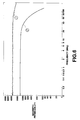
- Figure 7 is a graph showing the results of simulation of the magnetic field strength distribution in an MR head according to the present invention.
- An MR head of a first embodiment of the invention is an MR head in which a bias conductor for applying a bias magnetic field to a MR film is arranged on a MR film.
- an MR head has a lower shield layer 1 formed of a magnetic material, a lower gap layer 2 of a non-magnetic material formed on the lower shield layer 1, and an MR film 3 formed on one end of the lower gap layer 2.
- the MR head also has an upper gap layer 4 of a non-magnetic material formed on a forward portion of the MR film 3, that is, towards a medium contacting surface of the MR head, a flux guide 5 formed for being partially overlapped with the rear end of the MR film 3 and an insulating layer 6 formed on the MR layer 3 and on the flux guide 5.
- the MR head has a bias conductor 7 arranged within the interior of the insulating layer 6 for overlying the MR film 3, and an upper shield layer 8 of a magnetic material, formed on the upper gap layer 4 and the insulating layer 6.
- the lower shield layer 1, lower gap layer 2, upper gap layer 4 and the upper shield layer 8 serve to prohibit signal magnetic flux from the magnetic recording medium other than that to be reproduced from being captured into the MR film 3. That is, since the lower shield layer 1 and the upper shield layer 8 are arranged above and below the MR film 3 with the lower gap layer 2 and the upper gap layer 4 in-between, signal magnetic flux from the magnetic recording medium other than that to be reproduced is conducted to the lower shield layer 1 and the upper shield layer 8, such that only the magnetic flux to be reproduced is captured into the MR film 3.
- the upper gap layer 4 may be formed of an electrically conductive non-magnetic material and may be simultaneously used as the forward side electrode provided on the forward side of the MR film 3.
- the electrode disposed on the rear side of the MR film 3 may also be formed on the flux guide 5, or the flux guide 5 may be used simultaneously as the rear side electrode.
- the flux guide 5 is formed on the MR film 3 and the lower gap layer 2 so as to be partially overlapped with the rear end of the MR film 3, and is comprised of a laminated film structure of permalloy films 5b and Ti films 5c formed on the underlying layer 5a of Ta, as shown in Figure 2.
- the laminated film structure is designed so that the number of the permalloy films 5b is two or more and the uppermost and lowermost layers are the permalloy films 5b.
- the film thickness T1 of the permalloy film 5b is such that 0 nm ⁇ T1 ⁇ 50 nm and the film thickness T2 of the Ti film 5c is such that 0 nm ⁇ T2 ⁇ 6 nm.
- the film thickness T3 of the laminated film structure in its entirety is preferably on the order of 100 nm ⁇ T3 ⁇ 500 nm.
- the MR head of a second embodiment of the invention is an MR head in which a bias conductor for applying a bias magnetic field to the MR film is arranged below the MR film.
- the MR head of this second embodiment has a lower shield layer 11 of a magnetic material, a groove 11a formed in the lower shield layer 11 in registration with a MR film 13, as explained below, and a first insulating layer 16a formed in the inside of the groove 11a.
- the MR head also has a bias conductor 17 arranged in the inside of the first insulating layer 16a for underlying the MR film 13, as explained below, a lower gap layer 12 of a non-magnetic material formed on the lower shield layer 11, and the first insulating layer 16a and an MR film 13 formed towards one end of the gap layer 12.
- the MR head also has an upper gap layer 14 of a non-magnetic material formed at a forward end of the MR film 13, that is, towards the medium contacting surface of the MR head, a flux guide 15 formed so as to be partially overlapped with the rear end of the MR film 13, a second insulating layer 16b formed on the MR film 13 and the flux guide 15, and an upper shield layer 18 of a magnetic material formed on the upper gap layer 14 and the second insulating layer 16b.
- the MR head of the second embodiment is configured similarly to that of Example 1 except that the bias conductor 17 is arranged below the MR film 13.
- a flux guide was employed which was made up of six layers of permalloy films, each with film thickness of 50 nm, and six layers of Ti films, each with film thickness of 5 nm, laminated on a Ta underlying layer.
- FIGS. 4 and 5 show magnetization curves along the axis of easy magnetization and along the axis of hard magnetization, respectively. It was thus found that a coercive force Hc along the easy axis was 0.33 Oe, while that along the difficult axis was 0.24 Oe.
- the coercive force Hc with usual permalloy is on the order of 2 Oe.
- the present flux guide may be said to be superior in soft magnetic characteristics.
- the encircled numerals (3), (4), (5) and (6) denote curves for the flux guide being arranged at position 3 ⁇ m or more along the depth of the MR head from the medium contacting surface, for the flux guide being arranged at position 6 ⁇ m or more along the depth of the MR head from the medium contacting surface, for the flux guide being arranged at position 10 ⁇ m or more along the depth of the MR head from the medium contacting surface, and for the flux guide being not arranged, respectively. It is seen from these results that, by arraying the flux guide, the magnetic flux may be efficiently captured into the inside of the MR head.
- the intensity M of the magnetic field in the vicinity of the medium contacting surface is increased, so that, even if the length of the MR film along the depth of the MR head is reduced, a sufficient amount of the magnetic flux may be conducted to the MR film.
- the playback efficiency of the MR head may be improved by decreasing the length of the MR film for decreasing the impedance.
- the flux guide may be of a sole magnetic domain thereby assuring magnetic stability and high magnetic permeability on the order of 3000. The result is that the signal magnetic flux from the magnetic recording medium may be efficiently captured with stability into the MR film for improving the playback signal output of the MR head in stability.
- the flux guide employed in the present invention high magnetic permeability may be maintained in stability even at the high frequency range of tens of MHz.
- the magnetic flux capturing effect into the MR film by the flux guide may be produced in stability even if the recording signal on the magnetic recording medium is increased in frequency.
- the laminated film structure may be formed easily by continuous vapor deposition since the melting points of permalloy and Ti are both on the order of 1500° C.
- the flux guide may also be produced by the sputtering technique, instead of by continuous vapor deposition.
- the flux guide may be formed by any desired method which is in meeting with the MR head production process.
Landscapes
- Engineering & Computer Science (AREA)
- Manufacturing & Machinery (AREA)
- Magnetic Heads (AREA)
Applications Claiming Priority (3)
| Application Number | Priority Date | Filing Date | Title |
|---|---|---|---|
| JP14989194 | 1994-06-30 | ||
| JP6149891A JPH0817020A (ja) | 1994-06-30 | 1994-06-30 | 磁気抵抗効果型薄膜磁気ヘッド |
| JP149891/94 | 1994-06-30 |
Publications (3)
| Publication Number | Publication Date |
|---|---|
| EP0690438A2 true EP0690438A2 (de) | 1996-01-03 |
| EP0690438A3 EP0690438A3 (de) | 1996-06-19 |
| EP0690438B1 EP0690438B1 (de) | 2000-04-12 |
Family
ID=15484895
Family Applications (1)
| Application Number | Title | Priority Date | Filing Date |
|---|---|---|---|
| EP95110109A Expired - Lifetime EP0690438B1 (de) | 1994-06-30 | 1995-06-28 | Magneto-Widerstandseffekt-Dünnfilmmagnetkopf |
Country Status (5)
| Country | Link |
|---|---|
| US (1) | US5617276A (de) |
| EP (1) | EP0690438B1 (de) |
| JP (1) | JPH0817020A (de) |
| KR (1) | KR960002146A (de) |
| DE (1) | DE69516215T2 (de) |
Cited By (2)
| Publication number | Priority date | Publication date | Assignee | Title |
|---|---|---|---|---|
| WO2000062282A1 (en) * | 1999-04-14 | 2000-10-19 | Seagate Technology Llc | Highly sensitive spin valve heads using a self-aligned demag-field balance element |
| US6385016B1 (en) | 2000-03-31 | 2002-05-07 | Seagate Technology Llc | Magnetic read head with an insulator layer between an MR sensor and rear portions of current contacts to provide enhanced sensitivity |
Families Citing this family (12)
| Publication number | Priority date | Publication date | Assignee | Title |
|---|---|---|---|---|
| US5909344A (en) * | 1995-11-30 | 1999-06-01 | International Business Machines Corporation | Magnetoresistive sensor with high resistivity flux guide |
| JP2947172B2 (ja) * | 1996-05-23 | 1999-09-13 | ヤマハ株式会社 | 磁気抵抗効果型薄膜磁気ヘッド、誘導型・磁気抵抗効果型複合磁気ヘッド、磁気抵抗効果型薄膜磁気ヘッドの製造方法 |
| SG68063A1 (en) * | 1997-07-18 | 1999-10-19 | Hitachi Ltd | Magnetoresistive effect type reproducing head and magnetic disk apparatus equipped with the reproducing head |
| JP2000285417A (ja) * | 1999-03-31 | 2000-10-13 | Matsushita Electric Ind Co Ltd | 薄膜磁気ヘッド |
| JP3474523B2 (ja) | 2000-06-30 | 2003-12-08 | Tdk株式会社 | 薄膜磁気ヘッドおよびその製造方法 |
| JP2002133615A (ja) * | 2000-10-25 | 2002-05-10 | Sony Corp | 磁気抵抗効果型磁気ヘッド |
| JP2002260204A (ja) * | 2001-02-27 | 2002-09-13 | Fujitsu Ltd | 磁気ヘッド |
| US6680830B2 (en) | 2001-05-31 | 2004-01-20 | International Business Machines Corporation | Tunnel valve sensor and flux guide with improved flux transfer therebetween |
| US7057864B2 (en) | 2001-07-10 | 2006-06-06 | Hitachi Global Storage Technologies Netherlands B.V. | Method and apparatus for achieving physical connection between the flux guide and the free layer and that insulates the flux guide from the shields |
| US6783578B2 (en) * | 2002-12-17 | 2004-08-31 | Isolate, Inc. | Air purification unit |
| US7382574B2 (en) * | 2004-12-06 | 2008-06-03 | Seagate Technology Llc | Layered perpendicular writer with pole tip partially embedded in yoke |
| US7352540B1 (en) * | 2004-12-20 | 2008-04-01 | Storage Technology Corporation | Giant magneto-resistive (GMR) transducer having separation structure separating GMR sensor from head-tape interface |
Family Cites Families (15)
| Publication number | Priority date | Publication date | Assignee | Title |
|---|---|---|---|---|
| GB2003647B (en) * | 1977-09-02 | 1982-05-06 | Magnex Corp | Thin film magnetic recording heads |
| CA1137627A (en) * | 1978-04-25 | 1982-12-14 | Wilhelmus J. Van Gestel | Magnetoresistive head |
| NL8102148A (nl) * | 1981-05-01 | 1982-12-01 | Philips Nv | Magnetisch overdrachtselement alsmede magnetisch permeabel onderdeel voor een magnetisch overdrachtselement. |
| JPS61105717A (ja) * | 1984-10-26 | 1986-05-23 | Sanyo Electric Co Ltd | 磁気抵抗効果型磁気ヘツドの製造方法 |
| JPH0626009B2 (ja) * | 1984-11-20 | 1994-04-06 | 三洋電機株式会社 | 磁気抵抗効果型薄膜磁気ヘツドの製造方法 |
| US5111352A (en) * | 1987-07-29 | 1992-05-05 | Digital Equipment Corporation | Three-pole magnetic head with reduced flux leakage |
| US4816947A (en) * | 1987-11-12 | 1989-03-28 | International Business Machines | Single track vertical and horizontal recording read/write head design |
| US5032945A (en) * | 1989-11-07 | 1991-07-16 | International Business Machines Corp. | Magnetic thin film structures fabricated with edge closure layers |
| JPH03242983A (ja) * | 1990-02-06 | 1991-10-29 | Internatl Business Mach Corp <Ibm> | 磁気構造体の製造方法 |
| US5142426A (en) * | 1990-06-21 | 1992-08-25 | International Business Machines Corporation | Thin film magnetic head having interspersed resistance layers to provide a desired cut-off frequency |
| US5379172A (en) * | 1990-09-19 | 1995-01-03 | Seagate Technology, Inc. | Laminated leg for thin film magnetic transducer |
| JPH04214205A (ja) * | 1990-12-12 | 1992-08-05 | Fuji Electric Co Ltd | 薄膜磁気ヘッドおよびその製造方法 |
| US5465185A (en) * | 1993-10-15 | 1995-11-07 | International Business Machines Corporation | Magnetoresistive spin valve sensor with improved pinned ferromagnetic layer and magnetic recording system using the sensor |
| JPH07192227A (ja) * | 1993-12-28 | 1995-07-28 | Sony Corp | 磁気抵抗効果型磁気ヘッド |
| US5546254A (en) * | 1994-07-07 | 1996-08-13 | International Business Machines Corporation | Orthogonal MR Read head with single hard biased MR stripe |
-
1994
- 1994-06-30 JP JP6149891A patent/JPH0817020A/ja not_active Withdrawn
-
1995
- 1995-06-07 US US08/483,793 patent/US5617276A/en not_active Expired - Fee Related
- 1995-06-28 DE DE69516215T patent/DE69516215T2/de not_active Expired - Fee Related
- 1995-06-28 EP EP95110109A patent/EP0690438B1/de not_active Expired - Lifetime
- 1995-06-29 KR KR1019950018030A patent/KR960002146A/ko not_active Application Discontinuation
Non-Patent Citations (1)
| Title |
|---|
| None |
Cited By (3)
| Publication number | Priority date | Publication date | Assignee | Title |
|---|---|---|---|---|
| WO2000062282A1 (en) * | 1999-04-14 | 2000-10-19 | Seagate Technology Llc | Highly sensitive spin valve heads using a self-aligned demag-field balance element |
| GB2363513A (en) * | 1999-04-14 | 2001-12-19 | Seagate Technology Llc | Highly sensitive spin valve heads using a self-aligned demag-field balance element |
| US6385016B1 (en) | 2000-03-31 | 2002-05-07 | Seagate Technology Llc | Magnetic read head with an insulator layer between an MR sensor and rear portions of current contacts to provide enhanced sensitivity |
Also Published As
| Publication number | Publication date |
|---|---|
| JPH0817020A (ja) | 1996-01-19 |
| EP0690438A3 (de) | 1996-06-19 |
| DE69516215D1 (de) | 2000-05-18 |
| DE69516215T2 (de) | 2000-10-19 |
| EP0690438B1 (de) | 2000-04-12 |
| KR960002146A (ko) | 1996-01-26 |
| US5617276A (en) | 1997-04-01 |
Similar Documents
| Publication | Publication Date | Title |
|---|---|---|
| US5617276A (en) | Magneto-resistance effect thin-film magnetic head having a laminated flux guide of permalloy and titanium films | |
| US6721147B2 (en) | Longitudinally biased magnetoresistance effect magnetic head and magnetic reproducing apparatus | |
| JPH08153310A (ja) | 磁気抵抗効果型薄膜磁気ヘッド | |
| US5792546A (en) | Magneto-resistive head and method of producing the same | |
| US5600518A (en) | Magnetoresistive head having a stepped magnetoresistive film element | |
| JP3294742B2 (ja) | 磁気抵抗効果型ヘッド | |
| JP3475868B2 (ja) | 磁気抵抗効果型薄膜磁気ヘッド | |
| EP0756270B1 (de) | Dünnfilmmagnetkopf | |
| JP3678434B2 (ja) | 磁気抵抗効果型磁気ヘッドの製造方法 | |
| JPH0916916A (ja) | 薄膜磁気ヘッド及びその製造方法 | |
| JP2001256617A (ja) | 薄膜磁気ヘッド及びその製造方法 | |
| JPH09251616A (ja) | 薄膜磁気ヘッド | |
| JP2596010B2 (ja) | 磁気抵抗効果型磁気ヘッド | |
| JPH06267027A (ja) | 磁気抵抗効果型薄膜磁気ヘッド | |
| JPH0918069A (ja) | 磁気抵抗装置およびそれを形成するためのプロセス | |
| JPH08124122A (ja) | 磁気抵抗効果型再生ヘッドおよび磁気記録再生装置 | |
| JPH07296335A (ja) | 磁気抵抗型薄膜磁気ヘッド | |
| JPH05242433A (ja) | 磁気ヘッド | |
| JPH0944818A (ja) | 薄膜磁気ヘッド | |
| JP2001209914A (ja) | 磁気抵抗効果型薄膜磁気ヘッド及びその製造方法 | |
| JP2000132816A (ja) | 磁気抵抗効果型磁気ヘッド | |
| JPH1021511A (ja) | 磁気抵抗効果型磁気ヘッド | |
| JPH0441411B2 (de) | ||
| JPH0830925A (ja) | 磁気抵抗効果型薄膜磁気ヘッド | |
| JPH09251615A (ja) | 薄膜磁気ヘッド及びその製造方法 |
Legal Events
| Date | Code | Title | Description |
|---|---|---|---|
| PUAI | Public reference made under article 153(3) epc to a published international application that has entered the european phase |
Free format text: ORIGINAL CODE: 0009012 |
|
| AK | Designated contracting states |
Kind code of ref document: A2 Designated state(s): DE FR GB |
|
| K1C1 | Correction of patent application (title page) published |
Effective date: 19960103 |
|
| PUAL | Search report despatched |
Free format text: ORIGINAL CODE: 0009013 |
|
| AK | Designated contracting states |
Kind code of ref document: A3 Designated state(s): DE FR GB |
|
| 17P | Request for examination filed |
Effective date: 19961029 |
|
| 17Q | First examination report despatched |
Effective date: 19990325 |
|
| GRAG | Despatch of communication of intention to grant |
Free format text: ORIGINAL CODE: EPIDOS AGRA |
|
| GRAG | Despatch of communication of intention to grant |
Free format text: ORIGINAL CODE: EPIDOS AGRA |
|
| GRAG | Despatch of communication of intention to grant |
Free format text: ORIGINAL CODE: EPIDOS AGRA |
|
| GRAH | Despatch of communication of intention to grant a patent |
Free format text: ORIGINAL CODE: EPIDOS IGRA |
|
| GRAH | Despatch of communication of intention to grant a patent |
Free format text: ORIGINAL CODE: EPIDOS IGRA |
|
| GRAA | (expected) grant |
Free format text: ORIGINAL CODE: 0009210 |
|
| AK | Designated contracting states |
Kind code of ref document: B1 Designated state(s): DE FR GB |
|
| REF | Corresponds to: |
Ref document number: 69516215 Country of ref document: DE Date of ref document: 20000518 |
|
| ET | Fr: translation filed | ||
| PLBE | No opposition filed within time limit |
Free format text: ORIGINAL CODE: 0009261 |
|
| STAA | Information on the status of an ep patent application or granted ep patent |
Free format text: STATUS: NO OPPOSITION FILED WITHIN TIME LIMIT |
|
| 26N | No opposition filed | ||
| PGFP | Annual fee paid to national office [announced via postgrant information from national office to epo] |
Ref country code: FR Payment date: 20010611 Year of fee payment: 7 |
|
| PGFP | Annual fee paid to national office [announced via postgrant information from national office to epo] |
Ref country code: DE Payment date: 20010618 Year of fee payment: 7 |
|
| PGFP | Annual fee paid to national office [announced via postgrant information from national office to epo] |
Ref country code: GB Payment date: 20010627 Year of fee payment: 7 |
|
| REG | Reference to a national code |
Ref country code: GB Ref legal event code: IF02 |
|
| PG25 | Lapsed in a contracting state [announced via postgrant information from national office to epo] |
Ref country code: GB Free format text: LAPSE BECAUSE OF NON-PAYMENT OF DUE FEES Effective date: 20020628 |
|
| PG25 | Lapsed in a contracting state [announced via postgrant information from national office to epo] |
Ref country code: DE Free format text: LAPSE BECAUSE OF NON-PAYMENT OF DUE FEES Effective date: 20030101 |
|
| GBPC | Gb: european patent ceased through non-payment of renewal fee |
Effective date: 20020628 |
|
| PG25 | Lapsed in a contracting state [announced via postgrant information from national office to epo] |
Ref country code: FR Free format text: LAPSE BECAUSE OF NON-PAYMENT OF DUE FEES Effective date: 20030228 |
|
| REG | Reference to a national code |
Ref country code: FR Ref legal event code: ST |