EP0678992B1 - Générateur de signaux et système mobile sans fil l'incluant - Google Patents
Générateur de signaux et système mobile sans fil l'incluant Download PDFInfo
- Publication number
- EP0678992B1 EP0678992B1 EP95105926A EP95105926A EP0678992B1 EP 0678992 B1 EP0678992 B1 EP 0678992B1 EP 95105926 A EP95105926 A EP 95105926A EP 95105926 A EP95105926 A EP 95105926A EP 0678992 B1 EP0678992 B1 EP 0678992B1
- Authority
- EP
- European Patent Office
- Prior art keywords
- value
- signal
- correction
- output
- timer
- Prior art date
- Legal status (The legal status is an assumption and is not a legal conclusion. Google has not performed a legal analysis and makes no representation as to the accuracy of the status listed.)
- Expired - Lifetime
Links
Images


Classifications
-
- H—ELECTRICITY
- H03—ELECTRONIC CIRCUITRY
- H03K—PULSE TECHNIQUE
- H03K5/00—Manipulating of pulses not covered by one of the other main groups of this subclass
- H03K5/15—Arrangements in which pulses are delivered at different times at several outputs, i.e. pulse distributors
- H03K5/15013—Arrangements in which pulses are delivered at different times at several outputs, i.e. pulse distributors with more than two outputs
- H03K5/1502—Arrangements in which pulses are delivered at different times at several outputs, i.e. pulse distributors with more than two outputs programmable
-
- H—ELECTRICITY
- H04—ELECTRIC COMMUNICATION TECHNIQUE
- H04J—MULTIPLEX COMMUNICATION
- H04J3/00—Time-division multiplex systems
- H04J3/02—Details
- H04J3/06—Synchronising arrangements
- H04J3/0635—Clock or time synchronisation in a network
- H04J3/0685—Clock or time synchronisation in a node; Intranode synchronisation
-
- H—ELECTRICITY
- H04—ELECTRIC COMMUNICATION TECHNIQUE
- H04L—TRANSMISSION OF DIGITAL INFORMATION, e.g. TELEGRAPHIC COMMUNICATION
- H04L7/00—Arrangements for synchronising receiver with transmitter
- H04L7/04—Speed or phase control by synchronisation signals
- H04L7/08—Speed or phase control by synchronisation signals the synchronisation signals recurring cyclically
Definitions
- the present invention generally relates to a signal generator and a wireless (radio) mobile system 5 including such a signal generator. More specifically, the present invention is directed to a signal generator used to control TDMA (Time Division Multiple Access) type digital portable telephones, for generating signals at timings set within a constant time period, while easily controlling the timings of plural signals, and also to a radio mobile system employing such a general generator.
- TDMA Time Division Multiple Access
- control apparatuses require that signals are produced at timings preset within a constant time period.
- a signal generating apparatus capable of generating a signal at a preset timing there are typically two different types of signal generating apparatuses, i.e., one signal generating apparatus constructed by employing only the hardware, and the other signal generating apparatus by employing the hardware and the software.
- the former hardwared signal generator is superior to the latter hardwared/softwared signal generator.
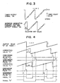
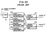
- Fig. 22 schematically shows one example of the conventional signal generating apparatus constructed of only the hardware, for generating two sets of signals "E" and "F” at preselected timings.
- This conventional hardwared signal generating apparatus is arranged by the timer 21 for counting time at a constant time period in response to the timer increment signal 22, the signal line constructed of a plurality of bit lines indicating the output value "r" of the timer 21, and the first to fourth coincidence detecting units 23 to 26 for comparing the output value of the timer 21 with the desired producing timing set in the internal data register to produce the coincidence detecting pulses s, t, u, v when the coincidence between them is made.
- This signal generating apparatus further includes the first and second output controlling units 27 and 28 for producing the signals "E" and "F” at the predetermined timings by using the coincidence detecting pulses s, t indicative of the timing producing commencements, outputted from the first and third coincidence detecting units 23, 24, and also the coincidence detecting pulses u, v representative of the timing producing completion, outputted from the second and fourth coincidence detecting units 25, 26.
- this conventional signal generating apparatus shown in Fig. 22 generates the two signals "E" and "F" at the predetermined timings, the total number of these coincidence detecting units and output controlling units may be further increased in order that a large number of signals at the preselected timings are produced.
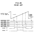
- Fig. 23 shows timing chart of this signal generating apparatus.
- the waveform of the output value "r" from the timer 21 is represented such that a change in the output values of this timer 21 is indicated in the ordinate when the time is indicated in the abscissa, and the count value of the timer 21 is counted up while the time elapses. It should be noted that since this counting up operation is digitally performed, this waveform of the timer output has actually a step shape, but this waveform is indicated in a straight line form for the sake of image representation.
- the first to fourth coincidence detecting units 23 to 26 produce the coincidence detecting pulses s, t, u, v when the output value "r" of the timer 21 is coincident with the values set in the respective coincidence detecting units 23 to 26.
- the coincidence detecting pulses s, u outputted from the first and second coincidence detecting units 23 and 25 are entered into the first output controlling unit 27.
- the first output controlling unit 27 controls the rising portion of the signal "E” based on this coincidence detecting pulse s, and also controls the falling portion of this signal "E” based upon the coincidence detecting pulse u, so that the signal "E” is produced.
- the coincidence detection pulses t and V outputted from the third and fourth coincidence detecting units 24 and 26 are entered into the second output controlling unit 28.
- the second output controlling unit 28 controls the rising portion of the signal "F” based on the coincidence detecting pulse t, and the falling portion of this signal "F” based upon the coincidence detecting pulse v.
- the positional data which are used to detect the coincidence and have been stored in the data registers provided inside the respective coincidence detecting units 23 to 26, is changed, so that the generation timings of the signals may be freely set.
- the conventional signal generating apparatus own such a problem. That is, when the generation timings of the plural signals are shifted by the same time amount at the same time, and also the generation time periods of the plural signals are simultaneously shifted by the same amount, such a control operation is necessarily required that both of the generating starting position and the generation ending position with respect to each of the plural signals are written into the registers employed in the coincidence detecting units. As a result, when the total number of signals generated from this conventional signal generating apparatus is increased, the more complex signal controlling operations would be required.
- the present invention has been made to solve these problems of the conventional signal generating apparatus, and therefore has an object to provide such a signal generating apparatus capable of effectively controlling both generation timings and generation ending timings for a large number of signals.
- the present invention starts from the teaching that is to be taken from WO-A-79100524.
- What is to be taken from said prior art document is a digital signal phase shifting system with a control means (66), said control means including a single correction means.
- EP-A-0464314 discloses a control device for radio communication apparatus including a timer circuit 20 and n comparing circuits 31 to 3n.
- a first signal generating apparatus of the present invention is such a signal generating apparatus for generating a signal whose generation starting timing and generation ending timing are controlled, and comprises:
- said control means includes first and second correction means for producing first and second correction values different from each other by correcting said timer output value; said coincidence detecting means outputs said coincidence detection pulses corresponding to said first and second correction values inputted from said control means, respectively; and said output control means controls the generation starting timing of said signal based on the coincidence detection pulse corresponding to said first correction value which is inputted from said coincidence detecting means, and also controls the generation ending timing of said signal based upon the coincidence detection pulse corresponding to said second correction value which is inputted from said coincidence detecting means.
- said first correction means includes:
- the first signal generating apparatus of the present invention when a plurality of signals are generated, for example, the first other set value stored in the first register and the second other set value stored in the second register are varied, and the correcting manner of the timer output value performed by the control means is changed.
- the generation positions of the plural signals can be simultaneously shifted by the same time, and also the generation periods of the plural signals can be simultaneously shifted by the same time.
- a second signal generating apparatus of the present invention is featured by that said correction means receives as an input value the output value of said first correction means.
- the second signal generating apparatus of the present invention when a plurality of signals are generated, only the generation positions of the plural signals can be simultaneously changed without changing the generation periods of the plural signals.
- a third signal generating apparatus of the present invention further comprises synchronization control means for resetting a count value of said timer in order that the count value of said timer is synchronized with an external condition.
- the synchronization control means when a plurality of signals are generated, resets the count value of the timer in adaptation to the external condition so as to correct the count value of the timer, so that the generation timings of all signals can be simultaneously changed.
- a fourth signal generating apparatus of the present invention comprises a plurality of said control means and said coincidence detecting means; and a set-value supply register for supplying said predetermined set value; and when said correction value inputted from corresponding one of said plural control means is coincidence with said set value inputted from said set-value supply register, each of said coincidence detecting means outputs a coincidence detection pulse.
- the timings of the plural signals generated in the different sequences can be simultaneously changed by merely changing the predetermined set value which is supplied from the set value supply register to the respective coincidence detecting means.
- a fifth signal generating apparatus of the present invention further comprises: a plurality of said output control means; and logic operation means for performing a logic operation of signals outputted from more than two arbitrary output control means among said plural output control means.
- the signals outputted from a plurality of output controlling means are OR-gated, or AND-gated, so that it is possible to produce such signals which raise at several times at a preselected timing during a predetermined time period.
- a sixth signal generating apparatus further comprises clock generating means for generating a clock signal; and clock logic operation means for performing a logic operation between the signal outputted from said output control means and said clock signal outputted from said clock generating means.
- the clock logic operation means OR-gates, or AND-gates the signal outputted from the output control means and the clock signal outputted from the clock generating means, so that the clock signal can be outputted during only such a time period when the signal outputted from the output control means becomes high, or low.
- said output control means includes a reset pulse register for outputting a reset pulse when a predetermined numeral value is written; starts to generate said signal when said coincidence detection pulse is inputted from said coincidence detecting means; and completes to generate said signal when said reset pulse is outputted from said reset pulse register.
- this seventh signal generating apparatus of the present invention since the generation of the signal is commenced in response to the coincidence detection pulse derived from the coincidence detecting means and also the generation of the signal is ended in response to the reset pulse derived from the reset pulse register, for instance, this seventh signal generating apparatus of the present invention may be utilized so as to periodically produce the interrupt signal to the CPU. In this case, for example, the CPU writes "o" into the reset pulse register when the interrupt process is completed, thereby outputting the reset pulse. Thus, the generation of this interrupt signal is ended.
- a wireless mobile apparatus is such a wireless mobile apparatus for transmitting/receiving a signal to/from a base station system.
- This wireless mobile apparatus comprises:
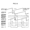
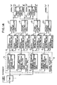
- a signal generating apparatus for generating four sets of signals "A”, “B”, “C”, “D", according to a first embodiment of the present invention, is comprised of a reference time timer 1 whose counting value is incremented in response to an externally supplied reference clock signals (timer increment signal 2), and a first sequence control unit 5 for controlling both of signal generation starting positions and signal generation ending positions for the two signals "A” and “B” at the same time while the two sets of signals "A” and "B” among the signals "A", “B", “C”, “D” are handled as one group (as a first sequence).
- This signal generating apparatus further includes a second sequence control unit 8 for simultaneously controlling both the signal generation starting position and the signal generation ending position of the signals "C” and “D” while the signals "C” and “D” are handled as one group (a second sequence).
- the first sequence control unit 5 is arranged by a first sequence generation starting position controlling unit 3 for controlling the output value of the timer 1 to output a correction value "b" so as to control the first sequence generation starting position, and a first sequence generation ending position controlling unit 4 for controlling the output value of the timer 1 to output another correction value "c" so as to control the first sequence generation ending position.
- the second sequence control unit 8 includes a second sequence generation starting position controlling unit 6 for controlling the output value of the timer 1 to output another correction value "j" in order to control the second sequence generation starting position, and a second sequence generation ending position controlling unit 7 for controlling the output of the timer 1 to output another correction value "k” in order to control the second sequence generation ending position.
- the signal generating apparatus is arranged by a first coincidence detecting unit 9 for comparing the setting position of starting the generation of the signal "A” with the correction value "b" of the timer 1 and for producing a coincidence detection pulse “d” when both values are coincident with each other, a second coincidence detecting unit 11 for comparing the setting position of ending the generation of the signal "A” with the correction value "c” and for producing a coincidence detection pulse “f” when both values are made coincident with each other, and further a first output controlling unit 17 for controlling a rising portion of the signal "A” and a falling portion thereof in response to the generation starting coincidence detection pulse "d” outputted from the first coincidence detecting unit 9 and the generation ending coincidence detection pulse “f” outputted from the second coincidence detecting unit 11, thereby producing the signal "A".
- the signal generating apparatus further includes a third coincidence detecting unit 10 for comparing the setting position of starting the generation of the signal "B" with the correction value "b" of the timer 1 and for producing a coincidence detection pulse “e” when both values are coincident with each other, a fourth coincidence detecting unit 12 for comparing the setting position of ending the generation of the signal “B” with the correction value "c” of the timer 1 and for producing a coincidence detection pulse “g” when both values are coincident with each other, and a second output controlling unit 18 for controlling a rising portion of the signal "B” and a falling portion thereof in response to the generation starting coincidence detection pulse "e” outputted from the third coincidence detecting unit 10 and the generation ending coincidence detection pulse "g” outputted from the four coincidence detecting unit 12, thereby producing the signal "B".
- a third coincidence detecting unit 10 for comparing the setting position of starting the generation of the signal "B" with the correction value "b” of the timer 1 and for producing a coincidence detection pulse “e” when both values are coinciden
- the signal generating apparatus is further comprised of a fifth coincidence detection unit 13 for comparing the setting position of starting the generation of the signal "C” with the correction value "j" of the timer 1 and for producing a coincidence detection pulse “l” when both values are coincident with each other, a sixth coincidence detecting unit 15 for comparing the setting position of ending the generation of the signal “C” with the correction value "k” and for producing a coincidence detection pulse “n” when both values are made coincident with each other, and further a third output controlling unit 19 for controlling a rising portion of the signal "C” and a falling portion thereof in response to the generation starting coincidence detection pulse "l” outputted from the fifth coincidence detecting unit 13 and the generation ending coincidence detection pulse “n” outputted from the sixth coincidence detecting unit 15, thereby producing the signal "C".
- the signal generating apparatus further includes a seventh coincidence detecting unit 14 for comparing the setting position of starting the generation of the signal "D" with the correction value "j" of the timer 1 and for producing a coincidence detection pulse “m” when both values are coincident with each other, an eighth coincidence detecting unit 16 for comparing the setting position of ending the generation of the signal “D” with the correction value "k” of the timer 1 and for producing a coincidence detection pulse “o” when both values are coincident with each other, and a fourth output controlling unit 20 for controlling a rising portion of the signal "D” and a falling portion thereof in response to the generation starting coincidence detection pulse "m” outputted from the seventh coincidence detecting unit 14 and the generation ending coincidence detection pulse “o” outputted from the eighth coincidence detecting unit 16, thereby producing the signal "D".
- each of the first sequence generation starting position controlling unit 3 employed in the first sequence control unit 5, and the second sequence generation starting position controlling unit 6 employed in the second sequence control unit 8 includes a register 30 for setting the sequence generation starting position, and a subtracter 29 for subtracting the set value of the register 30 from an input signal indicative of the value of the timer 1 (timer output signal 35).
- each of the first sequence generation ending position controlling unit 4 employed in the first sequence control unit 5 and the second sequence generation ending position controlling unit 7 employed in the second sequence control unit 8 includes a register 33 for setting the sequence generation ending position, and a subtracter 32 for subtracting the set value of the register 33 from the timer output signal 35.
- the first sequence control unit 5 and the second sequence control unit 8 corrects the value of the timer 1 as shown in Fig. 3.
- the value of the timer 1 is indicated by 3 bits.
- the timer 1 shown in Fig. 1 starts its counting operation from “000”, and then increments the count value by "1" every time one clock of the timer increment signal 2 is supplied. When the counting value reaches "111", this counting value is returned to "000". That is, the timer 1 outputs such a periodical counting value.
- an output signal 36 of the sequence generation starting position controlling unit is such a signal delayed by 2 clocks from the timer output signal 35.
- the respective coincidence detection pulses d, e, l, m are produced which each is delayed by 2 clocks with respect to the output signal of the timer 1.
- both the first sequence generation starting position controlling unit 3 and the second sequence generation starting position controlling unit 6 may delay and advance (quicken) the output signal from the timer 1 in response to the set value of the register.
- both the first sequence generation ending position controlling unit 4 of the first sequence control unit 5 and the second sequence generation ending position controlling unit 7 of the second sequence control unit 8 may delay and advance the output signal of the timer 1 in accordance with the set value of the register (register 33).
- circuits for setting the fixed value may be employed in the first sequence generation starting position controlling unit 3, the second sequence generation stating position controlling unit 6, the first sequence generation ending position controlling unit 4, and the second sequence generation ending position controlling unit 7.
- the correction value "b" outputted from the first sequence generation starting position controlling unit 3 is entered into the first coincidence detecting unit 9 and the third coincidence detecting unit 10, which control the generation starting positions of the signals "A" and “B", respectively.
- the first coincidence detecting unit 9 outputs the coincidence detection pulse "d” to the first output controlling unit 17.
- the third coincidence detecting unit 10 outputs the coincidence detection pulse "e” to the second output controlling unit 18.
- the first output controlling unit 17 controls the rising portion of the signal "A”.
- the second output controlling unit 18 controls the rising portion of the signal "B”.
- the correction value "c" outputted from the first sequence generation ending position controlling unit 4 is entered into the second coincidence detecting unit 11 and the fourth coincidence detecting unit 12, which control the generation ending positions of the signals "A" and “B", respectively.
- the second coincidence detecting unit 11 outputs the coincidence detection pulse "f" to the first output controlling unit 17.
- the fourth coincidence detecting unit 12 outputs the coincidence detection pulse "g" to the second output controlling unit 18.
- the first output controlling unit 17 controls the falling portion of the signal "A”.
- the second output controlling unit 18 controls the falling portion of the signal "B”.
- the signal "A” and the signal "B”, the rising timing and the falling timing of which are controlled are outputted from the first output controlling unit 17 and the second output controlling unit 18, respectively.
- the generation starting positions and the generation ending positions of the signal "A” and the signal “B” may be separately controlled by varying the data setting values used to determine the generation positions of the coincidence detection pulses "d" to "g” in the respective coincidence detecting units 9 to 12.
- the combination between the signal "A” and the signal “B” may be controlled in sequence unit by changing either the set value of the register 30 employed in the first sequence generation position controlling unit 3 of the first sequence control unit 5, or the set value of the register 33 employed in the first sequence generation ending position controlling unit 4.
- a total number of signals and also a total number of sequences may be freely increased/decreased by changing the combinations of these sequence control unit, coincidence detecting unit, and output controlling unit.
- the various signal generating apparatuses may be constructed by employing optimum circuits thereof.
- the rising portions and falling portions of the signals "A” to “D” are made coincident with the falling portions of the coincidence detection pulses.
- the rising portions and falling portions of these signals "A” to “D” may be again synchronized with the timer increment signal 2 with employment of flip-flop circuits and the like.
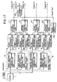
- a signal generating apparatus owns such a different arrangement from that of the signal generating apparatus according to the first embodiment of the present invention, shown in Fig. 1. That is, first, the first sequence control unit 5 includes a first sequence generation width controlling unit 38 instead of the first sequence generation ending position controlling unit 4. This first sequence generation width controlling unit 38 outputs a correction value "cc", which is obtained by further correcting the correction value "b" outputted from the first sequence generation starting position controlling unit 3, into the second and fourth coincidence detecting units 11 and 12. Secondly, the second sequence control unit 8 includes a second sequence generation width controlling unit 39 instead of the second sequence generation ending position controlling unit 7.
- This second sequence generation width controlling unit 39 outputs a correction value "kk", which is obtained by further correcting the correction value "j" outputted from the second sequence generation starting position controlling unit 6, into the sixth and eighth coincidence detecting units 15 and 16. It should be noted that each of the first sequence generation width controlling unit 38 and the second sequence generation width controlling unit 39 may be arranged by a subtracter and a register in a similar manner to the sequence generation ending position controlling unit 34 shown in Fig. 2.
- the correction value "b” is also supplied to the first sequence generation width controlling unit 38.
- the first sequence generation width controlling unit 38 outputs a correction value "cc" obtained by delaying this correction value "b" by time "zz".
- the correction value "cc” is inputted to the second coincidence detecting unit 11 and the fourth coincidence detecting unit 12, which control the generation ending positions of the signals "A" and “B", respectively.
- the second coincidence detecting unit 11 outputs the coincidence detection pulse “f” to the first output controlling unit 17 when the correction value "cc" is coincident with the internally set generation ending position data of the signal "A”.
- the fourth coincidence detecting unit 12 outputs the coincidence detection pulse “g” to the second output controlling unit 18 when the correction value "cc" is coincident with the internally set generation ending position data of the signal "B”.
- the first output controlling unit 17 control the falling portion of the signal "A” in response to the coincidence detection pulse "f", whereas the second output controlling unit 18 controls the falling portion of the signal "B” in response to the coincidence detection pulse "g".
- a signal generating apparatus owns such a different arrangement from that of the signal generating apparatus according to the first embodiment of the present invention as shown in Fig. 1. That is, a synchronization controlling unit 40 is interposed between the timer 1 and the first and second sequence control units 5 and 8, and this synchronization controlling unit 40 initiates the resetting operation of the timer 1 and outputs a corrected count value "aa" so as to make the count of the timer 1 coincident with the external condition.
- the timing of the final output signal is typically represented as the signal "A".
- the first sequence generation starting position controlling unit 3 and the first sequence generation ending position controlling unit 4, employed in the first sequence control unit 5 output a value identical to the corrected count value "aa” derived from the synchronization controlling unit 40 as a correction value "b" and another correction value "c", respectively.
- the first coincidence detecting unit 9 and the second coincidence detecting unit 11 output the coincidence detection pulses "d" and "f" at the fixed timing with respect to the correction values "b” and "c". Accordingly, the first output controlling unit 17 outputs the signal "A" at the fixed timing with respect to the corrected count value "aa”.
- Fig. 8 represents a timing of the signal "A” in case that no specific control is carried out in the synchronization controlling unit 40. Every time the count value of the timer 1 takes a constant timer count value "TC1", the synchronization controlling unit 40 'outputs a timer reset signal "tr” to the timer 1. As a consequence, the timer 1 repeats the counting operation at a constant period "T1", and the synchronization controlling unit 40 directly outputs the output value of the timer 1 as the corrected count value "aa”. Therefore, the signal "A" is generated with keeping the time period of "T1".
- both of the mode "1" and the count value (reset timing "TC2") of the timer 1 corresponding to the time “T2" used to delay the signal "A” are set to the synchronization controlling unit 40.
- the timer 1 continues the counting operation, and when the output value "a" of the timer 1 reaches the first timer count value "TC1" at time t 1 , the synchronization controlling unit 40 outputs the timer reset signal "tr" to the timer 1.
- the count value of the timer 1 which after the resetting operation, restarts its counting operation from the count value of "0" has reached the reset timing "TC2" at time t 2
- the synchronization controlling unit 40 again outputs the timer reset signal "tr” to the timer 1.
- the timer 1 Upon receipt of the timer reset signal "tr", the timer 1 resets the count value and restarts its counting operation from “0". Thereafter, every time the count value of the timer 1 reaches the timer count value "TC1", the synchronization control unit 40 outputs the timer reset signal "tr” and the timer 1 continues its counting operation at a time period of "T1".
- the synchronization controlling unit 40 While after the output value "a" of the timer 1 has reached the timer count value "TC1" immediately after setting the mode and then the timer 1 has been reset, the output value "a” of the timer 1 has reached the reset timing "TC2" to restart the resetting operation of the timer 1 (namely, a time duration from time t 1 to time t 2 ), the synchronization controlling unit 40 continues to output the fixed value "0" (otherwise, timer count value "TC1") as the corrected count value. Thereafter, this synchronization controlling unit 40 outputs the same value as the output value "a" of the timer 1.
- the signal “A” Since the generation starting timing and the generation ending timing of the signal “A" are measured on the basis of this corrected count value "aa", the signal “A” is delayed by the time “T2" during one time period after the mode setting operation, and the delayed signal “A” is outputted.
- mode 2 operation (mode 2) in case that the generation timing of the signal "A” is advanced, or quickened by the time “T3" in accordance with the externally supplied synchronization correction condition will now be described with reference to the timing chart shown in Fig. 10.
- the synchronization controlling unit 40 When the output value "a" of the timer 1 reaches the timer count value "TC1" at time t 1 after the mode setting operation, the synchronization controlling unit 40 resets the timer 1, and then when the output value "a” of the timer 1 reaches the count value "TC4" (i.e., at time t 2 ), again resets the timer 1. Thereafter, the synchronization controlling unit 40 repeats the resetting operation of the timer in the time period of "T1" in the normal operation. During this time duration, the synchronization controlling unit 40 outputs the same value as the output value "a" of the timer 1 as the corrected count value "aa".
- the signal “A” is raised when the output value “a” of the timer 1 reaches the count value “TC5" (TC5 ⁇ TC4) and also the signal “A” is lowered when the output value “a” of the timer 1 reaches the count value “TC6" (TC5 ⁇ TC6 ⁇ TC4), so that the generation timing of the signal “A” generated at the second timing after the mode setting operation can be quicken by the time "T3", as indicated in Fig. 10.
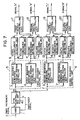
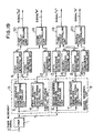
- a signal generating apparatus owns such a different arrangement, as compared with that of the signal generating apparatus according to the first embodiment of the present invention as shown in Fig. 1. That is, two sets of the above-described coincidence detecting units connected to the first sequence generation starting position controlling unit 3, and also two sets of the above-mentioned coincidence detecting units connected to the second sequence generation starting position controlling unit 6 commonly use one set-value supply register, whereas two sets of these coincidence detecting units connected to the first sequence generation ending position controlling unit 4 and also two sets of these coincidence detecting units connected to the second sequence generation starting point controlling unit 7 commonly use the other set-value supply register. As represented in Fig.
- both of a first coincidence detecting unit 43 for defining the generation timing of the signal "A”, and a fifth coincidence detecting unit 44 for defining the generation timing of the signal "C” commonly use a single piece of set-value supply register 45.
- the first coincidence detecting unit 43 is constructed of a first comparator 41 which outputs a coincidence detection pulse "d" when the correction value "b" derived from the first sequence generation starting position controlling unit 3 is compared with a predetermined set value "rr" derived from the set-value supply register 45, and then both of these values are coincident with each other.
- the fifth coincidence detecting unit 44 is constructed of a fifth comparator 42 which outputs a coincidence detection pulse "l" when the correction value "j" derived from the second sequence generation starting position controlling unit 6 is compared with a predetermined set value "rr” derived from the set-value supply register 45, and then both of these values are coincident with each other.
- the time duration defined by that the correction value "b" derived from the first sequence generation starting position controlling unit 3 starts from the count value “o” and then reaches the count value “TCI” is equal to the time duration defined by that the correction value "j" derived from the second sequence generation starting position controlling unit 6 starts from the count value "o” and then reaches the count value "TCI". It should be noted that this time duration is assumed as "TI”.
- both of the signal "A” and the signal “C” are produced with having such a delay time " ⁇ TI” required to increase the correction value "b” and the correction value “j” by the count value “ ⁇ TCI”, as compared with such a case that the set value "rr” of the set-value supply register 45 is set to the count value "TCI".
- the rising timings of the signal "A” and the signal “B” are delayed by the time “ ⁇ TI” from the time "TI".
- a signal generating apparatus has such a different arrangement from that of the signal generating apparatus according to the first embodiment, shown in Fig. 1. That is, this signal generating apparatus of the fifth embodiment is comprised of a first logic operation circuit 46 for performing a logic operation between the signal "A" outputted from the first output controlling unit 17 and the signal “C” outputted from the third output controlling unit 19 to produce a signal "G", and a second logic operation circuit 47 for performing a logic operation between the signal "B" outputted from the second output controlling unit 18 and the signal "C” outputted from the third output controlling unit 19 to produce a signal "H".
- Fig. 15 is a timing chart of the signals "A”, “B", “C”, “G”, “H” generated from the signal generating apparatus according to this embodiment when the first logic operation circuit 46 and the second logic operation circuit 47 are OR-gate circuits.
- the signal “G” outputted from the first logic operation circuit 46 corresponds to such a signal produced by OR-gating the signal “A” and the signal “C”
- the signal “H” outputted from the second logic operation circuit 47 corresponds to a signal obtained by OR-gating the signal "B” and the signal “C”.
- the signal “G” and the signal “H” are raised only two times at a predetermined timing within one time period of the signal "A".
- both of the first logic operation circuit 46 and the second logic operation circuit 47 are constructed of AND-gate circuits, so that it is possible to obtain two signals "G", "H” which are lowered plural times at a preselected timing during one time period of the signal "A".
- a signal processing apparatus owns such a different arrangement from that of the signal processing apparatus according to the first embodiment of the present invention, shown in Fig. 1. That is, this signal processing apparatus further includes a clock generating circuit 49 for generating a clock "CK", and a clock combining circuit 48 for combining the signal "A" outputted from the first output controlling unit 17 with the clock "CK” outputted from the clock generating circuit 49 to produce a signal "I”.
- the clock combining circuit 48 is arranged by such a logic operation circuit as an OR-gate circuit and an AND-gate circuit, and a circuit unit for suppressing hazard caused by timing shifts between the signal "A” and the clock "CK" while the signal "A” is combined with the clock "CK".
- the logic operation unit of the clock combining circuit 48 is arranged by an AND-gate circuit, so that as illustrated in the timing chart of Fig. 18, such a signal “I” having the same waveform as that of the clock “CK” only during the high-level period of the signal "A” can be generated.
- a signal generating apparatus owns the following different circuit arrangement, as compared with that of the signal generating apparatus indicated in Fig. 1, according to the first embodiment of the present invention. That is, the first output controlling unit 50 contains a reset pulse register 52 for outputting a reset pulse "RP" when a predetermined numeral value is written into this reset pulse register 52, starts to generate the signal "A” when the coincident detection pulse "d” from the first coincidence detecting unit 9 is entered therein, and completes to generate the signal "AA” when the reset pulse "RP" is outputted from the reset pulse register 52.
- the first output controlling unit 50 contains a reset pulse register 52 for outputting a reset pulse "RP" when a predetermined numeral value is written into this reset pulse register 52, starts to generate the signal "A” when the coincident detection pulse "d” from the first coincidence detecting unit 9 is entered therein, and completes to generate the signal "AA” when the reset pulse "RP” is outputted from the reset pulse register 52.
- the first output controlling unit 50 contains a reset
- the first output controlling unit 50 of the signal generating apparatus is constructed of the reset pulse register 52 for producing the reset pulse "RP" when "o” is written into this reset pulse register, and also a coincidence detection clear circuit 51 for raising the signal "AA” when the coincidence detection pulse “d” is inputted from the first coincident detecting unit 9 and for lowering the signal "AA” when the reset pulse "RP” is outputted from the reset pulse register 52.
- this signal generating apparatus may be employed as an apparatus for periodically generating an interrupt signal to a CPU.
- the interrupt signal to the CPU can be periodically produced in response to the coincidence detection pulse.
- the CPU will write "o" into the reset pulse register 52 so as to accomplish the generation of the interrupt signal, so that the interruption to the CPU can be released.
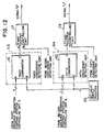
- Fig. 24 is a schematic block diagram for representing an arrangement of a wireless (radio) mobile apparatus according to an embodiment of the present invention.
- the wireless mobile apparatus 60 according to this embodiment is such a radio mobile system for transmitting and receiving the signals to/from a base station system 61 including a base station antenna 62, which includes an antenna 63 receives the electromagnetic waves transmitted from the base station system 61.
- the radio mobile apparatus 60 is arranged by as a reception unit thereof, a receiver 64 for receiving a signal, which is contains a baseband signal and is transmitted from the base station system 61, and also for extracting the baseband signal from the received signal; a demodulator 65 for demodulating the extracted baseband signal to reproduce a data series synchronized with the base station system 61; and a channel codec unit 66 functioning as an error correction decoding means for executing error correction decoding operation to the reproduced data series.
- the radio mobile apparatus 60 further includes a speech codec unit 67 functioning as an audio decoding means for decoding such audio data when the error-correction decoded data series corresponds to the audio data; a D/A converter 68 for digital-to-analog-converting the decoded audio data into an audio (voice) signal; and a speaker 69 for outputting the converted audio signal as a voice.
- a speech codec unit 67 functioning as an audio decoding means for decoding such audio data when the error-correction decoded data series corresponds to the audio data
- a D/A converter 68 for digital-to-analog-converting the decoded audio data into an audio (voice) signal
- a speaker 69 for outputting the converted audio signal as a voice.
- the radio mobile apparatus 60 is arranged by as a transmission unit, a microphone 70 for converting voice into an audio (voice) signal; an A/D converter 71 for analog-to-digital-converting the converted audio signal into audio data; the speech codec unit 67 functioning also as an audio encoding means for encoding the converted audio data; and the channel codec unit 66 functioning also as an error correction encoding means for error-correction encoding the encoded audio data.
- This radio mobile apparatus 60 further includes a modulator 72 for modulating the error-correction encoded audio data with a transmission carrier; and a transmitter 74 for transmitting the modulated audio data to the base station apparatus 61.
- the radio mobile apparatus 60 is constructed of as a control unit, a signal generating apparatus 74 for generating timing signals used to perform the signal transmitting/receiving operation of the radio mobile apparatus 60; a central processing unit (CPU) 75 for controlling the signal transmitting/receiving operation of the radio mobile apparatus 60; and a memory 76 for storing therein command data and control data used to the central processing unit 75.
- a signal generating apparatus 74 owns a similar arrangement to that of one of the above-explained signal generating apparatuses according to the first to seventh embodiments of the present invention.
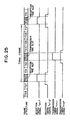
- Fig. 25 there is shown an example of a frame structure defined between the base station system 61 and the radio mobile apparatus 60, two sets of reception timing signals "RT1", “RT2” generated by the signal generating apparatus 74, and two sets of transmission timing signals "TT1", “TT2".
- RT1 reception timing signals
- RT2 transmission timing signals
- TT1 transmission timing signals
- a single TDMA (Time Division Multiple Access) frame is constructed of eight time slots “TS0" to "TS7".
- the time slot "TS0" is used as a reception time slot of the radio mobile apparatus 60
- the time slot "TS3" is used as a transmission time slot of the radio mobile apparatus 60.
- both the transmitting operation and the receiving operation of the radio mobile apparatus 60 are carried out in the time divisional manner.
- the signal generating apparatus 74 generates the reception timing signals "RT1", “RT2” at a timing located near the reception time slot, which will then be supplied to the receiver 64 and the demodulator 65, and also generates the transmission timing signals "TT1", “TT2” at a timing located near the transmission time slot, which will then be supplied to the modulator 72 and the transmitter 73.
- both the reception timing signals "RT1", “RT2” and the transmission timing signals "TT1", “TT2” may be generated at proper timings in accordance with the operations as previously explained in the signal generating apparatuses according to the first to seventh embodiments of the present invention by employing the signal generating apparatus 74 having an arrangement similar to that of one of the first to seventh signal generating apparatuses of the present invention. It should be understood that this signal generating apparatus 74 is controlled by the CPU 75.
Landscapes
- Engineering & Computer Science (AREA)
- Computer Networks & Wireless Communication (AREA)
- Signal Processing (AREA)
- Physics & Mathematics (AREA)
- Nonlinear Science (AREA)
- Synchronisation In Digital Transmission Systems (AREA)
- Mobile Radio Communication Systems (AREA)
- Electric Clocks (AREA)
- Time-Division Multiplex Systems (AREA)
- Programmable Controllers (AREA)
Claims (9)
- Appareil de génération de signaux pour générer un signal dont la temporisation de début de la génération et la temporisation de fin de la génération sont commandées, comprenant :caractérisé en ce queun temporisateur (1) pour produire une valeur de sortie du temporisateur en incrémentant ou en décrémentant une valeur de comptage en réponse à un signal d'horloge ;un moyen de commande (5, 8) ;un moyen de détection de coïncidence (9, 10, 13, 14 ; 11, 12, 15, 16) etun moyen de commande de sortie (17 à 20),
ledit moyen de commande (5, 8) inclut un premier moyen de correction (3, 6) et un deuxième moyen de correction (4, 8 ; 38, 39), ledit premier moyen de correction corrigeant ladite valeur de sortie du temporisateur pour produire une première valeur de correction, et ledit deuxième moyen de correction corrigeant ladite valeur de sortie du temporisateur ou ladite première valeur de correction pour produire une deuxième valeur de correction différente de ladite première valeur de correction ;
ledit moyen de détection de coïncidence inclut un premier moyen de détection de coïncidence (9, 10, 13, 14) pour comparer ladite première valeur de correction et une première valeur définie pour délivrer en sortie une première impulsion de détection de coïncidence lorsque ladite première valeur de correction coïncide avec ladite première valeur définie, et un deuxième moyen de détection de coïncidence (11, 12, 15, 16) pour comparer ladite deuxième valeur de correction et ladite deuxième valeur définie pour délivrer en sortie une deuxième impulsion de détection de coïncidence lorsque ladite deuxième valeur de correction coïncide avec ladite deuxième valeur définie ; et
ledit moyen de commande de sortie est adapté pour commander la temporisation de début de la génération dudit signal en réponse à ladite première impulsion de détection de coïncidence, et pour commander la temporisation de fin de la génération dudit signal en réponse à ladite deuxième impulsion de détection de coïncidence. - Appareil de génération de signaux selon la revendication 1, dans lequel :ledit premier moyen de correction (3, 6) inclut :un premier registre (30) pour stocker une troisième valeur définie ; etun premier soustracteur (29) pour soustraire ladite troisième valeur définie de ladite valeur de sortie du temporisateur pour produire ladite première valeur de correction ; etledit deuxième moyen de correction (4, 7) inclut :un deuxième registre (33) pour stocker une quatrième valeur définie ; etun deuxième soustracteur (32) pour soustraire ladite quatrième valeur définie de ladite valeur de sortie du temporisateur pour produire ladite deuxième valeur de correction.
- Appareil de génération de signaux selon la revendication 1 ou 2, comprenant de plus un moyen de commande de synchronisation (40) pour réinitialiser une valeur de comptage dudit temporisateur (1) afin que la valeur de comptage dudit temporisateur soit synchronisée avec une condition externe.
- Appareil de génération de signaux selon l'une quelconque des revendications précédentes comprenant de plus :un moyen de génération d'horloge (49) pour générer un autre signal d'horloge ; etun moyen d'opérations logiques d'horloge (48) pour effectuer une opération logique entre un signal de sortie dudit moyen de commande de sortie (17) et ledit autre signal d'horloge pour obtenir un signal pour commander au moins un parmi l'heure de début de la génération et l'heure de fin de la génération.
- Appareil de génération de signaux selon l'une quelconque des revendications précédentes, comprenant de plus un deuxième moyen de commande de sortie (50) pour commander la temporisation de début de la génération dudit signal en réponse à ladite première impulsion de détection de coïncidence, dans lequel :ledit deuxième moyen de commande de sortie (50) inclut un registre d'impulsions de réinitialisation (52) pour délivrer en sortie une impulsion de réinitialisation lorsqu'une valeur numérique prédéterminée est écrite dans ledit registre d'impulsions de réinitialisation par une unité centrale de traitement (75) et un moyen pour commander le temporisateur de fin de la génération dudit signal en réponse à ladite impulsion de réinitialisation.
- Appareil de génération de signaux selon l'une quelconque des revendications 1 à 4 comprenant :un troisième moyen de détection de coïncidence (43) pour comparer ladite première valeur de correction et une troisième valeur définie pour délivrer en sortie une troisième impulsion de détection de coïncidence lorsque ladite première valeur de correction coïncide avec ladite troisième valeur définie ;un quatrième moyen de détection de coïncidence (44) pour comparer ladite deuxième valeur de correction et une quatrième valeur définie pour délivrer en sortie une quatrième impulsion de détection de coïncidence lorsque ladite deuxième valeur de correction coïncide avec ladite quatrième valeur définie ;ledit moyen de commande de sortie comprenant :un premier moyen de commande de sortie (17) pour commander l'heure de début de la génération d'un premier signal en réponse à ladite première impulsion de détection de coïncidence, et pour commander la temporisation de fin de la génération dudit premier signal en réponse à ladite deuxième impulsion de détection de coïncidence ; etun deuxième moyen de commande de sortie (19) pour commander la temporisation de début de la génération d'un deuxième signal en réponse à ladite troisième impulsion de détection de coïncidence, et pour commander la temporisation de fin de la génération dudit deuxième signal en réponse à ladite quatrième impulsion de détection de coïncidence.
- Appareil de génération de signaux selon la revendication 6, dans lequel
le premier moyen de commande (5) ayant un premier moyen de correction (3) et un deuxième moyen de correction (6), ledit premier moyen de correction corrigeant ladite valeur de sortie du temporisateur pour produire une première valeur de correction et ledit deuxième moyen de correction corrigeant ladite valeur de sortie du temporisateur ou ladite première valeur de correction pour produire une deuxième valeur de correction différente de ladite première valeur de correction ;
le deuxième moyen de commande (8) ayant un troisième moyen de correction (4) et un quatrième moyen de correction (7), ledit troisième moyen de correction corrigeant ladite valeur de sortie du temporisateur pour produire une troisième valeur de correction, et ledit quatrième moyen de correction corrigeant ladite valeur de sortie du temporisateur ou ladite troisième valeur de correction pour produire une quatrième valeur de correction différente de ladite troisième valeur de correction. - Appareil de génération de signaux selon la revendication 6 ou 7, dans lequel :ladite première valeur définie et ladite troisième valeur définie ont une même valeur ; etledit appareil de génération de signaux comprend de plus un registre fournissant des valeurs définies (45) pour fournir lesdites première et troisième valeurs définies auxdits premier et troisième moyens de détection de coïncidence.
- Appareil de génération de signaux selon l'une quelconque des revendications 6 à 8, dans lequel :ladite deuxième valeur définie et ladite quatrième valeur définie ont une même valeur ; etledit appareil de génération de signaux comprend de plus un autre registre fournissant des valeurs définies (45) pour fournir lesdites deuxième et quatrième valeurs définies auxdits deuxième et quatrième moyens de détection de coïncidence.
Applications Claiming Priority (6)
| Application Number | Priority Date | Filing Date | Title |
|---|---|---|---|
| JP10633294 | 1994-04-22 | ||
| JP10633294 | 1994-04-22 | ||
| JP106332/94 | 1994-04-22 | ||
| JP27724694A JP3534457B2 (ja) | 1994-04-22 | 1994-10-18 | 信号発生装置 |
| JP277246/94 | 1994-10-18 | ||
| JP27724694 | 1994-10-18 |
Publications (3)
| Publication Number | Publication Date |
|---|---|
| EP0678992A2 EP0678992A2 (fr) | 1995-10-25 |
| EP0678992A3 EP0678992A3 (fr) | 1998-07-01 |
| EP0678992B1 true EP0678992B1 (fr) | 2003-11-05 |
Family
ID=26446448
Family Applications (1)
| Application Number | Title | Priority Date | Filing Date |
|---|---|---|---|
| EP95105926A Expired - Lifetime EP0678992B1 (fr) | 1994-04-22 | 1995-04-20 | Générateur de signaux et système mobile sans fil l'incluant |
Country Status (8)
| Country | Link |
|---|---|
| US (1) | US5719906A (fr) |
| EP (1) | EP0678992B1 (fr) |
| JP (1) | JP3534457B2 (fr) |
| CN (1) | CN1082777C (fr) |
| DE (1) | DE69532056T2 (fr) |
| FI (1) | FI113816B (fr) |
| NO (1) | NO951499L (fr) |
| SG (1) | SG52144A1 (fr) |
Families Citing this family (9)
| Publication number | Priority date | Publication date | Assignee | Title |
|---|---|---|---|---|
| US6014569A (en) * | 1997-03-05 | 2000-01-11 | At&T Corp. | Mobile interactive radio |
| WO1999059247A1 (fr) * | 1998-05-11 | 1999-11-18 | Infineon Technologies Ag | Dispositif et procede de synchronisation |
| US6037821A (en) * | 1998-05-28 | 2000-03-14 | General Electric Company | Digital programmable clock generator with improved accuracy |
| US20020091848A1 (en) * | 2000-09-06 | 2002-07-11 | Robert Agresta | System, device and method for remotely providing, accessing and using personal entertainment media |
| JP4016709B2 (ja) * | 2002-04-26 | 2007-12-05 | 日本電気株式会社 | オーディオデータの符号変換伝送方法と符号変換受信方法及び装置とシステムならびにプログラム |
| KR20040015457A (ko) * | 2002-08-13 | 2004-02-19 | 현대모비스 주식회사 | 제어 주기가 다른 여러 개의 작업을 제어하는 방법 |
| CN104811194B (zh) * | 2012-01-09 | 2018-05-01 | 青岛海信移动通信技术股份有限公司 | 一种集中式时钟装置和移动终端设备 |
| CN103869813B (zh) * | 2012-12-14 | 2017-02-01 | 苏州宝时得电动工具有限公司 | 自动工作系统 |
| US9503102B2 (en) * | 2014-08-29 | 2016-11-22 | Tektronix, Inc. | Synchronization for multiple arbitrary waveform generators |
Family Cites Families (6)
| Publication number | Priority date | Publication date | Assignee | Title |
|---|---|---|---|---|
| US4180778A (en) * | 1978-01-18 | 1979-12-25 | The Singer Company | Digital signal phase shifting system |
| US4295098A (en) * | 1979-12-19 | 1981-10-13 | Rca Corporation | Digitally adjustable phase shifting circuit |
| CA1227844A (fr) * | 1983-09-07 | 1987-10-06 | Michael T.H. Hewitt | Reseau de transmission a noeud unique et a plusieurs stations de sortie |
| US5185880A (en) * | 1989-06-05 | 1993-02-09 | Matsushita Electric Industrial Co., Ltd. | Stored instructions executing type timing signal generating system |
| JP2836637B2 (ja) * | 1990-07-06 | 1998-12-14 | 三菱電機株式会社 | 無線通信機の制御装置 |
| JP2723691B2 (ja) * | 1991-04-30 | 1998-03-09 | 日本電気株式会社 | 可変タイミング信号発生回路 |
-
1994
- 1994-10-18 JP JP27724694A patent/JP3534457B2/ja not_active Expired - Fee Related
-
1995
- 1995-04-11 US US08/420,154 patent/US5719906A/en not_active Expired - Lifetime
- 1995-04-19 SG SG1995000280A patent/SG52144A1/en unknown
- 1995-04-20 DE DE69532056T patent/DE69532056T2/de not_active Expired - Fee Related
- 1995-04-20 EP EP95105926A patent/EP0678992B1/fr not_active Expired - Lifetime
- 1995-04-20 NO NO951499A patent/NO951499L/no not_active Application Discontinuation
- 1995-04-21 CN CN95104714A patent/CN1082777C/zh not_active Expired - Fee Related
- 1995-04-21 FI FI951906A patent/FI113816B/fi not_active IP Right Cessation
Also Published As
| Publication number | Publication date |
|---|---|
| EP0678992A2 (fr) | 1995-10-25 |
| FI113816B (fi) | 2004-06-15 |
| FI951906A0 (fi) | 1995-04-21 |
| DE69532056T2 (de) | 2004-08-26 |
| FI951906A7 (fi) | 1995-10-23 |
| SG52144A1 (en) | 1998-09-28 |
| EP0678992A3 (fr) | 1998-07-01 |
| JPH088696A (ja) | 1996-01-12 |
| DE69532056D1 (de) | 2003-12-11 |
| NO951499L (no) | 1995-10-23 |
| HK1003555A1 (en) | 1998-10-30 |
| CN1082777C (zh) | 2002-04-10 |
| NO951499D0 (no) | 1995-04-20 |
| JP3534457B2 (ja) | 2004-06-07 |
| US5719906A (en) | 1998-02-17 |
| CN1112347A (zh) | 1995-11-22 |
Similar Documents
| Publication | Publication Date | Title |
|---|---|---|
| EP0678992B1 (fr) | Générateur de signaux et système mobile sans fil l'incluant | |
| US5276713A (en) | Method of frame synchronization for digital mobile radio communication | |
| HK1003555B (en) | Signal generator and wireless mobile system including the same | |
| JP2693758B2 (ja) | フレームパルス発生方式 | |
| WO2000031915A3 (fr) | Procede et circuit de reajustement du rythme d'un signal de donnees numeriques | |
| US5146478A (en) | Method and apparatus for receiving a binary digital signal | |
| JP2762941B2 (ja) | 背景雑音発生装置 | |
| US5252972A (en) | Codec having controllable frame synchronizing and clocking signals | |
| CA1065409A (fr) | Reduction du taux d'erreurs dans les circuits de radioteleimprimeurs | |
| JP2967649B2 (ja) | 受信同期回路 | |
| JPH0226135A (ja) | 移動無線装置 | |
| JPS5819056A (ja) | クロツク再生回路 | |
| JPS60214142A (ja) | 変調装置 | |
| KR0176139B1 (ko) | 비트 동기회로 | |
| JP3929830B2 (ja) | 揺らぎ補正装置および揺らぎ補正方法 | |
| KR0172459B1 (ko) | 클럭재생방법 및 장치 | |
| JPH01133441A (ja) | クロック同期方式 | |
| KR970009685B1 (ko) | 무선기지국의 특정신호 듀티싸이클 조정 회로 | |
| JP2962288B2 (ja) | ディジタルコードレス電話機 | |
| JPH06188853A (ja) | アパーチャ幅可変同期検出回路 | |
| JPH024535Y2 (fr) | ||
| JPH05207003A (ja) | フレーム同期信号検出回路 | |
| JPS5854694B2 (ja) | クロック位相選択回路 | |
| JPH0222572B2 (fr) | ||
| JPH0433412A (ja) | リタイミング回路 |
Legal Events
| Date | Code | Title | Description |
|---|---|---|---|
| PUAI | Public reference made under article 153(3) epc to a published international application that has entered the european phase |
Free format text: ORIGINAL CODE: 0009012 |
|
| 17P | Request for examination filed |
Effective date: 19950427 |
|
| AK | Designated contracting states |
Kind code of ref document: A2 Designated state(s): DE FR GB IT SE |
|
| PUAL | Search report despatched |
Free format text: ORIGINAL CODE: 0009013 |
|
| AK | Designated contracting states |
Kind code of ref document: A3 Designated state(s): DE FR GB IT SE |
|
| 17Q | First examination report despatched |
Effective date: 20020304 |
|
| GRAH | Despatch of communication of intention to grant a patent |
Free format text: ORIGINAL CODE: EPIDOS IGRA |
|
| GRAS | Grant fee paid |
Free format text: ORIGINAL CODE: EPIDOSNIGR3 |
|
| GRAA | (expected) grant |
Free format text: ORIGINAL CODE: 0009210 |
|
| AK | Designated contracting states |
Kind code of ref document: B1 Designated state(s): DE FR GB IT SE |
|
| REG | Reference to a national code |
Ref country code: GB Ref legal event code: FG4D |
|
| REF | Corresponds to: |
Ref document number: 69532056 Country of ref document: DE Date of ref document: 20031211 Kind code of ref document: P |
|
| REG | Reference to a national code |
Ref country code: SE Ref legal event code: TRGR |
|
| ET | Fr: translation filed | ||
| PLBE | No opposition filed within time limit |
Free format text: ORIGINAL CODE: 0009261 |
|
| 26N | No opposition filed |
Effective date: 20040806 |
|
| PGFP | Annual fee paid to national office [announced via postgrant information from national office to epo] |
Ref country code: SE Payment date: 20070404 Year of fee payment: 13 |
|
| PGFP | Annual fee paid to national office [announced via postgrant information from national office to epo] |
Ref country code: DE Payment date: 20070412 Year of fee payment: 13 |
|
| PGFP | Annual fee paid to national office [announced via postgrant information from national office to epo] |
Ref country code: GB Payment date: 20070418 Year of fee payment: 13 |
|
| PGFP | Annual fee paid to national office [announced via postgrant information from national office to epo] |
Ref country code: IT Payment date: 20070601 Year of fee payment: 13 |
|
| PGFP | Annual fee paid to national office [announced via postgrant information from national office to epo] |
Ref country code: FR Payment date: 20070411 Year of fee payment: 13 |
|
| EUG | Se: european patent has lapsed | ||
| GBPC | Gb: european patent ceased through non-payment of renewal fee |
Effective date: 20080420 |
|
| PG25 | Lapsed in a contracting state [announced via postgrant information from national office to epo] |
Ref country code: DE Free format text: LAPSE BECAUSE OF NON-PAYMENT OF DUE FEES Effective date: 20081101 |
|
| REG | Reference to a national code |
Ref country code: FR Ref legal event code: ST Effective date: 20081231 |
|
| PG25 | Lapsed in a contracting state [announced via postgrant information from national office to epo] |
Ref country code: FR Free format text: LAPSE BECAUSE OF NON-PAYMENT OF DUE FEES Effective date: 20080430 |
|
| PG25 | Lapsed in a contracting state [announced via postgrant information from national office to epo] |
Ref country code: GB Free format text: LAPSE BECAUSE OF NON-PAYMENT OF DUE FEES Effective date: 20080420 |
|
| PG25 | Lapsed in a contracting state [announced via postgrant information from national office to epo] |
Ref country code: IT Free format text: LAPSE BECAUSE OF NON-PAYMENT OF DUE FEES Effective date: 20080420 |
|
| PG25 | Lapsed in a contracting state [announced via postgrant information from national office to epo] |
Ref country code: SE Free format text: LAPSE BECAUSE OF NON-PAYMENT OF DUE FEES Effective date: 20080421 |