EP0661582A2 - Afficheur à cristal liquide - Google Patents
Afficheur à cristal liquide Download PDFInfo
- Publication number
- EP0661582A2 EP0661582A2 EP94309743A EP94309743A EP0661582A2 EP 0661582 A2 EP0661582 A2 EP 0661582A2 EP 94309743 A EP94309743 A EP 94309743A EP 94309743 A EP94309743 A EP 94309743A EP 0661582 A2 EP0661582 A2 EP 0661582A2
- Authority
- EP
- European Patent Office
- Prior art keywords
- liquid crystal
- crystal display
- display according
- layers
- transistors
- Prior art date
- Legal status (The legal status is an assumption and is not a legal conclusion. Google has not performed a legal analysis and makes no representation as to the accuracy of the status listed.)
- Granted
Links
- 239000004973 liquid crystal related substance Substances 0.000 title claims abstract description 101
- 239000004065 semiconductor Substances 0.000 claims abstract description 51
- 239000011159 matrix material Substances 0.000 claims abstract description 25
- 239000000758 substrate Substances 0.000 claims abstract description 25
- 239000010410 layer Substances 0.000 claims description 178
- 229910021420 polycrystalline silicon Inorganic materials 0.000 claims description 31
- 229910052751 metal Inorganic materials 0.000 claims description 14
- 239000002184 metal Substances 0.000 claims description 14
- 239000010409 thin film Substances 0.000 claims description 7
- 230000015572 biosynthetic process Effects 0.000 claims description 4
- 229910021419 crystalline silicon Inorganic materials 0.000 claims 2
- 238000009751 slip forming Methods 0.000 claims 1
- 239000010408 film Substances 0.000 description 40
- 238000000034 method Methods 0.000 description 12
- 230000005684 electric field Effects 0.000 description 9
- 238000005530 etching Methods 0.000 description 9
- 239000011521 glass Substances 0.000 description 9
- 239000012535 impurity Substances 0.000 description 8
- 238000010438 heat treatment Methods 0.000 description 6
- 230000001105 regulatory effect Effects 0.000 description 5
- 239000010936 titanium Substances 0.000 description 5
- 108091006146 Channels Proteins 0.000 description 4
- KRHYYFGTRYWZRS-UHFFFAOYSA-N Fluorane Chemical compound F KRHYYFGTRYWZRS-UHFFFAOYSA-N 0.000 description 4
- 239000005380 borophosphosilicate glass Substances 0.000 description 4
- 238000005229 chemical vapour deposition Methods 0.000 description 4
- 230000007423 decrease Effects 0.000 description 4
- 230000007547 defect Effects 0.000 description 4
- 239000011229 interlayer Substances 0.000 description 4
- 238000004519 manufacturing process Methods 0.000 description 4
- 238000005070 sampling Methods 0.000 description 4
- WGTYBPLFGIVFAS-UHFFFAOYSA-M tetramethylammonium hydroxide Chemical compound [OH-].C[N+](C)(C)C WGTYBPLFGIVFAS-UHFFFAOYSA-M 0.000 description 4
- QTBSBXVTEAMEQO-UHFFFAOYSA-N Acetic acid Chemical compound CC(O)=O QTBSBXVTEAMEQO-UHFFFAOYSA-N 0.000 description 3
- 229910018125 Al-Si Inorganic materials 0.000 description 3
- 229910018520 Al—Si Inorganic materials 0.000 description 3
- 229910018594 Si-Cu Inorganic materials 0.000 description 3
- VYPSYNLAJGMNEJ-UHFFFAOYSA-N Silicium dioxide Chemical compound O=[Si]=O VYPSYNLAJGMNEJ-UHFFFAOYSA-N 0.000 description 3
- 229910008465 Si—Cu Inorganic materials 0.000 description 3
- 230000003247 decreasing effect Effects 0.000 description 3
- 239000000463 material Substances 0.000 description 3
- 238000002161 passivation Methods 0.000 description 3
- 238000000059 patterning Methods 0.000 description 3
- 230000002093 peripheral effect Effects 0.000 description 3
- 229910021426 porous silicon Inorganic materials 0.000 description 3
- 239000000243 solution Substances 0.000 description 3
- 229910052719 titanium Inorganic materials 0.000 description 3
- 229910008599 TiW Inorganic materials 0.000 description 2
- ATJFFYVFTNAWJD-UHFFFAOYSA-N Tin Chemical compound [Sn] ATJFFYVFTNAWJD-UHFFFAOYSA-N 0.000 description 2
- 229910052782 aluminium Inorganic materials 0.000 description 2
- 238000000137 annealing Methods 0.000 description 2
- 239000013078 crystal Substances 0.000 description 2
- 238000000151 deposition Methods 0.000 description 2
- 230000008021 deposition Effects 0.000 description 2
- 230000006866 deterioration Effects 0.000 description 2
- 238000009792 diffusion process Methods 0.000 description 2
- 239000007789 gas Substances 0.000 description 2
- 150000002500 ions Chemical class 0.000 description 2
- 239000007788 liquid Substances 0.000 description 2
- 229910021421 monocrystalline silicon Inorganic materials 0.000 description 2
- 238000005498 polishing Methods 0.000 description 2
- 229920001721 polyimide Polymers 0.000 description 2
- 238000002360 preparation method Methods 0.000 description 2
- 238000004544 sputter deposition Methods 0.000 description 2
- 239000000126 substance Substances 0.000 description 2
- 229910052715 tantalum Inorganic materials 0.000 description 2
- ZOXJGFHDIHLPTG-UHFFFAOYSA-N Boron Chemical compound [B] ZOXJGFHDIHLPTG-UHFFFAOYSA-N 0.000 description 1
- 229910001218 Gallium arsenide Inorganic materials 0.000 description 1
- MHAJPDPJQMAIIY-UHFFFAOYSA-N Hydrogen peroxide Chemical compound OO MHAJPDPJQMAIIY-UHFFFAOYSA-N 0.000 description 1
- ZOKXTWBITQBERF-UHFFFAOYSA-N Molybdenum Chemical compound [Mo] ZOKXTWBITQBERF-UHFFFAOYSA-N 0.000 description 1
- 108010075750 P-Type Calcium Channels Proteins 0.000 description 1
- OAICVXFJPJFONN-UHFFFAOYSA-N Phosphorus Chemical compound [P] OAICVXFJPJFONN-UHFFFAOYSA-N 0.000 description 1
- 229910007264 Si2H6 Inorganic materials 0.000 description 1
- BLRPTPMANUNPDV-UHFFFAOYSA-N Silane Chemical compound [SiH4] BLRPTPMANUNPDV-UHFFFAOYSA-N 0.000 description 1
- XUIMIQQOPSSXEZ-UHFFFAOYSA-N Silicon Chemical compound [Si] XUIMIQQOPSSXEZ-UHFFFAOYSA-N 0.000 description 1
- RTAQQCXQSZGOHL-UHFFFAOYSA-N Titanium Chemical compound [Ti] RTAQQCXQSZGOHL-UHFFFAOYSA-N 0.000 description 1
- 239000000853 adhesive Substances 0.000 description 1
- 230000001070 adhesive effect Effects 0.000 description 1
- 229910021417 amorphous silicon Inorganic materials 0.000 description 1
- 229910052785 arsenic Inorganic materials 0.000 description 1
- RQNWIZPPADIBDY-UHFFFAOYSA-N arsenic atom Chemical compound [As] RQNWIZPPADIBDY-UHFFFAOYSA-N 0.000 description 1
- QVGXLLKOCUKJST-UHFFFAOYSA-N atomic oxygen Chemical compound [O] QVGXLLKOCUKJST-UHFFFAOYSA-N 0.000 description 1
- 229910052796 boron Inorganic materials 0.000 description 1
- 239000003990 capacitor Substances 0.000 description 1
- 238000004140 cleaning Methods 0.000 description 1
- 239000003086 colorant Substances 0.000 description 1
- 238000004040 coloring Methods 0.000 description 1
- 238000002425 crystallisation Methods 0.000 description 1
- 230000008025 crystallization Effects 0.000 description 1
- 230000002950 deficient Effects 0.000 description 1
- PZPGRFITIJYNEJ-UHFFFAOYSA-N disilane Chemical compound [SiH3][SiH3] PZPGRFITIJYNEJ-UHFFFAOYSA-N 0.000 description 1
- 230000000694 effects Effects 0.000 description 1
- BVDPFTQTMQKPGQ-UHFFFAOYSA-N ethanol hydrofluoride Chemical compound F.CCO BVDPFTQTMQKPGQ-UHFFFAOYSA-N 0.000 description 1
- 238000000227 grinding Methods 0.000 description 1
- 238000003384 imaging method Methods 0.000 description 1
- AMGQUBHHOARCQH-UHFFFAOYSA-N indium;oxotin Chemical compound [In].[Sn]=O AMGQUBHHOARCQH-UHFFFAOYSA-N 0.000 description 1
- 230000005764 inhibitory process Effects 0.000 description 1
- 238000002347 injection Methods 0.000 description 1
- 239000007924 injection Substances 0.000 description 1
- 238000011835 investigation Methods 0.000 description 1
- 239000005001 laminate film Substances 0.000 description 1
- 238000002844 melting Methods 0.000 description 1
- 239000011259 mixed solution Substances 0.000 description 1
- 238000002156 mixing Methods 0.000 description 1
- 239000000203 mixture Substances 0.000 description 1
- 229910052750 molybdenum Inorganic materials 0.000 description 1
- 239000011733 molybdenum Substances 0.000 description 1
- 239000001301 oxygen Substances 0.000 description 1
- 229910052760 oxygen Inorganic materials 0.000 description 1
- 230000003071 parasitic effect Effects 0.000 description 1
- 229910052698 phosphorus Inorganic materials 0.000 description 1
- 239000011574 phosphorus Substances 0.000 description 1
- 230000002265 prevention Effects 0.000 description 1
- 230000002035 prolonged effect Effects 0.000 description 1
- 239000011347 resin Substances 0.000 description 1
- 229920005989 resin Polymers 0.000 description 1
- 230000002441 reversible effect Effects 0.000 description 1
- 229910021332 silicide Inorganic materials 0.000 description 1
- FVBUAEGBCNSCDD-UHFFFAOYSA-N silicide(4-) Chemical compound [Si-4] FVBUAEGBCNSCDD-UHFFFAOYSA-N 0.000 description 1
- 229910052710 silicon Inorganic materials 0.000 description 1
- 239000010703 silicon Substances 0.000 description 1
- 239000007787 solid Substances 0.000 description 1
- 239000007790 solid phase Substances 0.000 description 1
- WFKWXMTUELFFGS-UHFFFAOYSA-N tungsten Chemical compound [W] WFKWXMTUELFFGS-UHFFFAOYSA-N 0.000 description 1
- 229910052721 tungsten Inorganic materials 0.000 description 1
- 239000010937 tungsten Substances 0.000 description 1
Images


Classifications
-
- H—ELECTRICITY
- H01—ELECTRIC ELEMENTS
- H01L—SEMICONDUCTOR DEVICES NOT COVERED BY CLASS H10
- H01L29/00—Semiconductor devices specially adapted for rectifying, amplifying, oscillating or switching and having potential barriers; Capacitors or resistors having potential barriers, e.g. a PN-junction depletion layer or carrier concentration layer; Details of semiconductor bodies or of electrodes thereof ; Multistep manufacturing processes therefor
- H01L29/66—Types of semiconductor device ; Multistep manufacturing processes therefor
- H01L29/68—Types of semiconductor device ; Multistep manufacturing processes therefor controllable by only the electric current supplied, or only the electric potential applied, to an electrode which does not carry the current to be rectified, amplified or switched
- H01L29/76—Unipolar devices, e.g. field effect transistors
- H01L29/772—Field effect transistors
- H01L29/78—Field effect transistors with field effect produced by an insulated gate
- H01L29/786—Thin film transistors, i.e. transistors with a channel being at least partly a thin film
- H01L29/78606—Thin film transistors, i.e. transistors with a channel being at least partly a thin film with supplementary region or layer in the thin film or in the insulated bulk substrate supporting it for controlling or increasing the safety of the device
- H01L29/78612—Thin film transistors, i.e. transistors with a channel being at least partly a thin film with supplementary region or layer in the thin film or in the insulated bulk substrate supporting it for controlling or increasing the safety of the device for preventing the kink- or the snapback effect, e.g. discharging the minority carriers of the channel region for preventing bipolar effect
- H01L29/78615—Thin film transistors, i.e. transistors with a channel being at least partly a thin film with supplementary region or layer in the thin film or in the insulated bulk substrate supporting it for controlling or increasing the safety of the device for preventing the kink- or the snapback effect, e.g. discharging the minority carriers of the channel region for preventing bipolar effect with a body contact
-
- G—PHYSICS
- G02—OPTICS
- G02F—OPTICAL DEVICES OR ARRANGEMENTS FOR THE CONTROL OF LIGHT BY MODIFICATION OF THE OPTICAL PROPERTIES OF THE MEDIA OF THE ELEMENTS INVOLVED THEREIN; NON-LINEAR OPTICS; FREQUENCY-CHANGING OF LIGHT; OPTICAL LOGIC ELEMENTS; OPTICAL ANALOGUE/DIGITAL CONVERTERS
- G02F1/00—Devices or arrangements for the control of the intensity, colour, phase, polarisation or direction of light arriving from an independent light source, e.g. switching, gating or modulating; Non-linear optics
- G02F1/01—Devices or arrangements for the control of the intensity, colour, phase, polarisation or direction of light arriving from an independent light source, e.g. switching, gating or modulating; Non-linear optics for the control of the intensity, phase, polarisation or colour
- G02F1/13—Devices or arrangements for the control of the intensity, colour, phase, polarisation or direction of light arriving from an independent light source, e.g. switching, gating or modulating; Non-linear optics for the control of the intensity, phase, polarisation or colour based on liquid crystals, e.g. single liquid crystal display cells
- G02F1/133—Constructional arrangements; Operation of liquid crystal cells; Circuit arrangements
- G02F1/1333—Constructional arrangements; Manufacturing methods
- G02F1/1345—Conductors connecting electrodes to cell terminals
- G02F1/13454—Drivers integrated on the active matrix substrate
-
- H—ELECTRICITY
- H01—ELECTRIC ELEMENTS
- H01L—SEMICONDUCTOR DEVICES NOT COVERED BY CLASS H10
- H01L27/00—Devices consisting of a plurality of semiconductor or other solid-state components formed in or on a common substrate
- H01L27/02—Devices consisting of a plurality of semiconductor or other solid-state components formed in or on a common substrate including semiconductor components specially adapted for rectifying, oscillating, amplifying or switching and having potential barriers; including integrated passive circuit elements having potential barriers
- H01L27/12—Devices consisting of a plurality of semiconductor or other solid-state components formed in or on a common substrate including semiconductor components specially adapted for rectifying, oscillating, amplifying or switching and having potential barriers; including integrated passive circuit elements having potential barriers the substrate being other than a semiconductor body, e.g. an insulating body
- H01L27/1203—Devices consisting of a plurality of semiconductor or other solid-state components formed in or on a common substrate including semiconductor components specially adapted for rectifying, oscillating, amplifying or switching and having potential barriers; including integrated passive circuit elements having potential barriers the substrate being other than a semiconductor body, e.g. an insulating body the substrate comprising an insulating body on a semiconductor body, e.g. SOI
-
- G—PHYSICS
- G02—OPTICS
- G02F—OPTICAL DEVICES OR ARRANGEMENTS FOR THE CONTROL OF LIGHT BY MODIFICATION OF THE OPTICAL PROPERTIES OF THE MEDIA OF THE ELEMENTS INVOLVED THEREIN; NON-LINEAR OPTICS; FREQUENCY-CHANGING OF LIGHT; OPTICAL LOGIC ELEMENTS; OPTICAL ANALOGUE/DIGITAL CONVERTERS
- G02F1/00—Devices or arrangements for the control of the intensity, colour, phase, polarisation or direction of light arriving from an independent light source, e.g. switching, gating or modulating; Non-linear optics
- G02F1/01—Devices or arrangements for the control of the intensity, colour, phase, polarisation or direction of light arriving from an independent light source, e.g. switching, gating or modulating; Non-linear optics for the control of the intensity, phase, polarisation or colour
- G02F1/13—Devices or arrangements for the control of the intensity, colour, phase, polarisation or direction of light arriving from an independent light source, e.g. switching, gating or modulating; Non-linear optics for the control of the intensity, phase, polarisation or colour based on liquid crystals, e.g. single liquid crystal display cells
- G02F1/133—Constructional arrangements; Operation of liquid crystal cells; Circuit arrangements
- G02F1/136—Liquid crystal cells structurally associated with a semi-conducting layer or substrate, e.g. cells forming part of an integrated circuit
- G02F1/1362—Active matrix addressed cells
- G02F1/136213—Storage capacitors associated with the pixel electrode
-
- H—ELECTRICITY
- H01—ELECTRIC ELEMENTS
- H01L—SEMICONDUCTOR DEVICES NOT COVERED BY CLASS H10
- H01L29/00—Semiconductor devices specially adapted for rectifying, amplifying, oscillating or switching and having potential barriers; Capacitors or resistors having potential barriers, e.g. a PN-junction depletion layer or carrier concentration layer; Details of semiconductor bodies or of electrodes thereof ; Multistep manufacturing processes therefor
- H01L29/66—Types of semiconductor device ; Multistep manufacturing processes therefor
- H01L29/68—Types of semiconductor device ; Multistep manufacturing processes therefor controllable by only the electric current supplied, or only the electric potential applied, to an electrode which does not carry the current to be rectified, amplified or switched
- H01L29/76—Unipolar devices, e.g. field effect transistors
- H01L29/772—Field effect transistors
- H01L29/78—Field effect transistors with field effect produced by an insulated gate
- H01L29/786—Thin film transistors, i.e. transistors with a channel being at least partly a thin film
- H01L29/78606—Thin film transistors, i.e. transistors with a channel being at least partly a thin film with supplementary region or layer in the thin film or in the insulated bulk substrate supporting it for controlling or increasing the safety of the device
- H01L29/78618—Thin film transistors, i.e. transistors with a channel being at least partly a thin film with supplementary region or layer in the thin film or in the insulated bulk substrate supporting it for controlling or increasing the safety of the device characterised by the drain or the source properties, e.g. the doping structure, the composition, the sectional shape or the contact structure
Definitions
- the present invention relates to a liquid crystal display equipped with an active matrix circuit board.
- liquid crystal display for displaying, for example, television images by the use of a high-density two-dimensional matrix liquid crystal display (an active matrix type liquid crystal display) in which a thin film transistor (TFT) is utilized.
- TFT thin film transistor
- liquid crystal display in which switching elements comprising the poly-Si TFTs are used has the following problems.
- An object of the present invention is to provide a liquid crystal display which can solve the above-mentioned problems and which can exert a high contrast, a high gradation and a high resolution.
- Another object of the present invention is to provide a liquid crystal display having a high reliability and a high yield.
- Still another object of the present invention is to provide a TFT structure and its peripheral structure for realizing the liquid crystal display having the above-mentioned excellent characteristics.
- the present invention has been attained by intensively conducting investigation with the intention of solving the above-mentioned problems, and it has the undermentioned constitution.
- a liquid crystal display which comprises an active matrix circuit board equipped with a plurality of transistors having a plurality of pixel electrodes arranged along a plurality of lines and rows and drains connected to these pixel electrodes, scanning lines for commonly connecting gates of the transistors arranged along the lines, and signal lines for commonly connecting sources of the transistors arranged along the rows; a substrate having a facing electrode; and a liquid crystal interposed between the active matrix circuit board and the substrate.
- the liquid crystal display being constituted so that a voltage may be applied to regions of a conductive mode which is different from a conductive mode of the sources and the drains of semiconductor layers constituting the transistors.
- the liquid crystal display of the present invention includes a liquid crystal display, wherein capacitors have one terminals connected to the drains of the transistors, and the other terminals not connected to the drain but connected to the regions (hereinafter also referred to as "wells") of a conductive mode different from a conductive mode of the sources and the drains of semiconductor layers constituting the transistors.
- a poor carrier generated in a high electric field or a light carrier generated owing to light leakage flows to a power source connected to the wells, so that the fluctuation of a well potential does not occur.
- a TFT leakage current is much smaller as compared with a conventional case, so that the signal of the pixel electrodes does not change, thereby realizing a high contrast and a high gradation.
- the potential change of the pixel electrodes can be further prevented by the capacities, even if the similar leakage current of the TFTs is generated. In consequence, the high contrast and the high gradation can be realized.
- the liquid crystal display of the present invention has excellent characteristics such as a low flicker, good temperature properties, a stable operation, a clear display due to the increased aperture ratio, the enlargement of a view angle, the decrease of image deterioration by external light and a good compatibility with a panel having a large number of the pixels.
- the semiconductor layers having the formed transistors comprise the poly-Si or a single crystal Si, for example, a shift register, a bias regulating circuit, a gain regulating circuit or the like can be arranged on the periphery of the liquid crystal panel, so that the manufacturing cost of the panel can be decreased.
- the liquid crystal display of the present invention having the above-mentioned excellent characteristics can be applied to an electronic view finder for VTR incorporated into a camera, a display panel for a computer or a word processor, a head mounted display, a display panel for projection TV, a display panel for a meter such as an oscilloscope, a display panel for a handy terminal, a display panel for TV conference and TV telephone, and the like.
- Fig. 1 is an equivalent circuit illustrating one embodiment of a liquid crystal display of the present invention.
- Fig. 2 is a schematic view illustrating one embodiment of an active matrix circuit board which can be applied to the liquid crystal display of the present invention.
- Fig. 3 is a schematic view illustrating one embodiment of a constitution of the liquid crystal display of the present invention.
- Fig. 4 is an equivalent circuit illustrating another embodiment of the liquid crystal display of the present invention.
- Fig. 5 is an equivalent circuit illustrating still another embodiment of the liquid crystal display of the present invention.
- Fig. 6 is a schematic view illustrating another embodiment of the active matrix circuit board which can be applied to the liquid crystal display of the present invention.
- Fig. 7 is an enlarged view in which a region A in Fig. 6 is enlarged.
- Figs. 8A to 8J are schematic views illustrating one embodiment of a manufacturing process of the liquid crystal display of the present invention.
- Figs. 9A to 9E are schematic views illustrating another embodiment of a manufacturing process of the liquid crystal display of the present invention.
- Fig. 10 is a schematic view illustrating still another embodiment of the active matrix circuit board which can be applied to the liquid crystal display of the present invention.
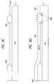
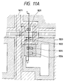
- Figs. 11A is a schematic view illustrating a further embodiment of the active matrix circuit board which can be applied to the liquid crystal display of the present invention.
- Fig. 11B and 11C are sectional views taken along the line Y-Y' of the circuit board shown in Fig. 11A.
- Fig. 12 is a schematic view illustrating another embodiment of a constitution of the liquid crystal display of the present invention.
- Fig. 1 is an equivalent circuit for a liquid crystal display of the present invention.
- reference numeral 1 is a liquid crystal layer
- numeral 2 is a facing electrode arranged on a substrate facing to an active matrix circuit board on which a TFT is placed
- 11, 12 and 13 are signal lines
- 21 and 22 are scanning lines.
- Numerals 31 and 32 are power source lines for fixing the potential of TFT wells, and they are connected in common in a periphery of a display region and further connected to a power source terminal 33.
- Numerals 41, 42 and 43 are sampling transistors
- 51 is a horizontal signal line
- 61 is a horizontal shift register
- 71 is a vertical shift register.
- Numerals 111, 112, 113, 121, 122 and 123 are gate electrodes of the TFTs placed in pixel divisions, and these gate electrodes are connected to the scanning lines 21, 22.
- Numerals 211, 212, 213, 221, 222 and 223 are regions (wells) other than sources ⁇ drains of semiconductor layers constituting the respective TFTs, and these wells are connected to the power source lines 31, 32.
- Numerals 311, 312, 313, 321, 322 and 323 are sources of the respective TFTs, and they are connected to the signal lines 11, 12 and 13, respectively.
- Numerals 411, 412, 413, 421, 422 and 423 are drains of the respective TFTs, and they are connected to pixel electrodes 511, 512, 513, 521, 522 and 523, respectively.
- n-type (n-channel MOS) and p-type (p-channel MOS) are both usable.
- a voltage applied between the pixel electrode and the facing electrode is usually about ⁇ 5 V, and between the source and the drain, a voltage of about 10 V is applied. Therefore, from the viewpoint of voltage resistance, the p-type TFT having a small impact ionization rate is preferable.
- a video signal from a solid imaging device, a broadcast or the like is input to the horizontal signal line 51.
- Fig. 1 shows an example in which only one horizontal signal line is present, but in the case of a color display or the like, a plurality of horizontal signal lines of desired colors for a red signal, a blue signal, a green signal and the like may be arranged.
- the video signals input to the horizontal signal line 51 are selected in turn in compliance with scanning pulses from the horizontal shift register 61 by the respective sampling transistors 41, 42, 43.
- the input video signals are written in turn to the pixel electrodes 511, 512, 513 via the signal lines 11, 12, 13. Therefore, in the case that the TFTs placed in the pixel divisions are the p-type, a voltage is applied from the power source terminal 33 so that a well potential may be more than a maximum of the amplitude of the video signals. Furthermore, in the case that the TFTs are the n-type, a voltage is applied from the source terminal 33 so that the well potential may be less than a minimum of the amplitude of the video signals.
- the potential of the scanning line 21 is regulated by the vertical shift register 71 to be at a level at which the TFTs in the pixel divisions are switched off. The same drive is carried out for the line of the next scanning line 22.
- Fig. 2 shows a plan view of an active matrix circuit board which can be applied to the liquid crystal display of the present invention.
- the signal line 11 is connected to the p+ layers 311, 321 of the source divisions of the TFTs via contacts.
- the signal line 12 is connected to the p+ layers 312, 322 via contacts.
- the signal lines 11, 12 are made up of a metal wire of Al, Al-Si, Al-Si-Cu or the like.
- the p+ layers 311, 611, 312, 612 are each arranged in the vicinity of the center of the source ⁇ drain division of the semiconductor layer constituting the TFT, and n+ layers 1011, 1012 having a high concentration are each arranged in its periphery. These highly concentrated layers are held sufficiently apart from each other in consideration of voltage resistance. In the case of this embodiment, a space of 1.5 to 2.5 ⁇ m is given between these layers.
- the n wells are present between the p+ layers 311, 611, 312, 612 and the n+ layers 1011, 1012, and for the relief of an electric field between the n+ layer and the p+ layer, p ⁇ layers may be formed in the peripheries of the p+ layers.
- the signals fed to the signal lines 11, 12 are transmitted through the sources to the drains of the TFTs which can be operated via the scanning line 21.
- p ⁇ layers 1111, 1112 are formed between the sources and gates, and between the drains and the gates in order to relieve the electric field between the sources and the gates and between the drains and the gates.
- the scanning lines 21, 22 are usually made up of a poly-Si, but in order to obtain the high-speed drive and satisfactory shading on the scanning lines, it is desirable to use a polysilicide such as tungsten polysilicide, titanium polysilicide or molybdenum polysilicide.
- drain electrodes 711, 712 are arranged, and they are connected to the p+ layers 611, 612, respectively.
- the drain electrodes are made up of layers of the same wires as the signal lines, and the semiconductor divisions constituting the TFTs are covered with these wiring layers and the scanning lines, whereby the semiconductor divisions constituting the TFTs are shaded.
- a signal voltage is transmitted to the pixel electrodes 511, 512 via through-holes 811, 812.
- n+ layers 1011, 1012 having a high concentration d are arranged in the peripheries of the semiconductor divisions constituting the TFTs, and these n+ layers are also arranged along the signal lines to connect the n+ layers to a desired power source, thereby taking the well potential of the TFTs.
- FIG. 3 A sectional view cut along the line Y-Y' in Fig. 2 is shown in Fig. 3.
- the semiconductor layer constituting the TFT is placed on a glass substrate 3, and in the periphery of the semiconductor division constituting the TFT of the semiconductor layer, the n+ layer 1011 is arranged.
- the semiconductor layer comprises the n-type well, and since the semiconductor layer and the n+ layer 1011 have the same kind of conductive mode, there is no problem, even if the highly concentrated n+ layer 1011 is not always diffused to a boundary between the n+ layer 1011 and the glass substrate 4.
- liquid crystal display of this embodiment there is employed a structure in which no junction region is present in the periphery of the semiconductor layer, and thus any current is not generated from a defective layer which is formed in the case that the junction region is placed, so that the TFT in which a leakage current is inhibited can be obtained.
- the interlayer insulating layer can be made up of an SiN film formed by the use of a vacuum CVD method, PSG which is a phosphorus-doped glass, or a boron phosphorus-doped glass.
- a laminate which can be used to constitute the liquid crystal display panel is prepared by superposing films having tensile stress or compressive stress upon each other.
- the films obtained by the above-mentioned vacuum CVD method have the strength tensile stress, and so the warpage of the liquid crystal display panel can be controlled by regulating the thickness of these films to a desired value.
- Numerals 11 and 711 are metal wiring layers, but in order to sufficiently heighten the adhesive state of the metal wiring layers, it is desirable to form BPSG under the metal wiring layers.
- the metal wiring layers are each preferably prepared by superposing a film of Ti, Ta, TiW, Mo, TiN, TaN or the like upon a wire of Al, Al-Si, Al-Si-Cu or the like.
- the thus prepared metal wiring layers are desirable, because the contact resistance of ITO or the like which becomes the pixel electrode is low, and ohmic properties and stability can be obtained.
- the insulating layer of PSG or the like is deposited to flatten an etch back and the like.
- the pixel electrode 511 is formed by a sputtering process.
- the surface of the metal wire Prior to the film formation of a transparent electrode ITO (indium tin oxide) for the pixel electrode by the use of the sputtering process, the surface of the metal wire is preferably cleaned by presputtering. This cleaning operation realizes a good ohmic connection between the pixel electrode 511 and the metal wiring layer 711 which is the drain electrode.
- ITO indium tin oxide
- the orientation film may comprise a one-layer structure or a multi-layer structure by which a view angle is enlarged.
- a facing substrate is constituted by the following procedure.
- a layer 10 for shading a step portion of the TFT is formed on the glass substrate 200, while a space between the pixels is regulated, and color filter layers 9 are patterned so as to be separated by the pixels, as shown in Fig. 3, whereby a problem of color mixing between the color filters can be avoided.
- a transparent electrode which is a common electrode and an orientation film 8 are formed to obtain the facing substrate.
- a liquid crystal 7 is confined to constitute the liquid crystal display panel.
- polarizing plates and the like are not shown, but the polarizing plates are arranged on the outer surfaces of both the substrates.
- a voltage is applied to a semiconductor layer region having the same conductive mode as in the well of the semiconductor constituting the TFT to fix a well potential. Then, on the side wall of the semiconductor region constituting the TFT, an impurity region having a conductive mode opposite to the source ⁇ drain is formed.
- the leakage current of the TFT can be reduced, so that the display having a high contrast and a high gradation can be realized.
- defects due to damage caused at the time of a manufacturing process can be decreased, and the liquid crystal display panel which exerts a stable operation can be obtained in a high yield.
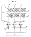
- Fig. 4 shows an equivalent circuit
- the same parts as in an equivalent circuit shown in Fig. 1 are represented by the same reference numerals and their detailed description will be omitted.
- the liquid crystal display of this embodiment is different from a liquid crystal display of Example 1 in that wires 34, 35 for fixing a potential in a region (well) having a conductive mode different from that of a source ⁇ drain of a semiconductor layer constituting a TFT are arranged along scanning lines 21, 22, and a common connection is made in the periphery of a pixel panel, and video signals are sampled by the use of CMOS analog switches 44, 45 and 46.
- the liquid crystal display panel In the case that the liquid crystal display panel is driven, it is effective for the inhibition of flicker that the voltage to be applied to the liquid crystal every line is reversed. In this case, a strong electric field takes place in a line direction extending between the pixel electrodes on each line, i.e., a longitudinal direction, so that a line defect called discrimination occurs, with the result that blank areas appear irrespective of the voltage to be applied to the pixel electrode and contrast deteriorates. Therefore, for the liquid crystal display capable of displaying an image with a high contrast, it is important that a space between pixel aperture regions in the longitudinal direction is set so as to be wider than in the transverse direction.
- the wires 34, 35 for fixing the well potential are arranged in a horizontal direction, so that the region where the blank areas tend to appear is effectively shaded, and the reverse drive is also possible. In consequence, the pixel display having the good contrast and the less flicker can be realized.
- the sampling of the video signals is carried out by the use of the CMOS analog switches 44, 45 and 46, and the well potentials of the CMOS analog switches are also set to suitable values for the n-type and p-type TFTs, respectively.
- Reference numerals 36 and 38 are wires for fixing the well potentials, and numerals 37 and 39 are power sources for these wires.
- the video signals can be sampled and fed to the signal lines independently of threshold values of the sampling transistors and the like, and therefore a panel drive voltage can be lowered to enhance reliability owing to the enlargement of a voltage resistance margin and to increase the freedom of the design of peripheral circuits.
- the freedom of connections to other ICs increases, and the decrease of cost can also be achieved.
- Fig. 5 shows an equivalent circuit
- the same parts as in an equivalent circuit shown in Fig. 1 are represented by the same reference numerals and their detailed description will be omitted.
- This embodiment is characterized in that capacities 1211, 1212, 1213, 1221, 1222, 1223 for holding a voltage in each pixel are installed, and terminals of these capacities are connected to the drain electrodes of TFTs and the other terminals of these capacities are connected to electrodes 34, 35 having a well potential of the TFTs.
- the potential of the drain terminal of the TFT changes owing to the responsibility of the liquid crystal, deflection caused by on and off of the TFT and a leakage current of the TFT.
- the sufficient capacities which are not affected by these causes are arranged in pixel divisions, whereby a good and stable image display can be realized.
- liquid crystal display of this embodiment will be described with reference to a plan view shown in Fig. 6.
- signal lines 11, 12 are arranged, while shifted as much as a 1/2 pixel every line for the purpose of the improvement of resolution and coloring properties, and these signal lines are non-linear.
- Source divisions 311, 312, drain divisions 611, 612 or gate divisions are arranged, being protruded from scanning lines 21, 22, and the arrangement direction of the source ⁇ drain extends along the scanning lines.
- Fig. 7 shows a detailed view of a periphery of a region surrounded by a dotted line A. Description will be made with reference to Fig. 7 in addition to Fig. 6.
- a highly concentrated impurity layer 1301 having the same conductive mode as in a well is formed in upward, downward, right and left directions except a part of a lower portion in which an opening 1800 of a panel, the source division, the drain division, the scanning line and the signal line are arranged.
- the potential contacts a wiring layer in the periphery of the panel opening 1800, so that it is fixed.
- a capacity forming member 1303 is formed via an insulating layer.
- the capacity forming member 1303 is made up of a poly-Si polysilicide, a high-melting metal or the like. This capacity forming member 1303 is used to form the capacity between the capacity forming member 1303 and the highly concentrated impurity layer 1301.
- the signal forwarded to the drain division is fed to the capacity forming member 1303 at a contact division via the wire.
- one terminal of the capacity forming member 1303 is connected to the drain division of the TFT, and the other terminal of the capacity forming member 1303 is connected to the well division of the TFT.
- a shading layer is formed on the front side of this paper except the portion of the opening 1800.
- the shading layer can be made up of an insulating layer or a conductive layer.
- a TaN film is used.
- the TaN film is a conductive layer, and therefore if the TaN film contacts the drain or the pixel electrode, the signal is not transmitted to the pixel electrode. Accordingly, a hole 1422 is formed around a through-hole 1522 for connecting the pixel electrode to the drain division.
- the pixel electrode potential is more stable, and a high-quality image display can be realized.
- Figs. 8A to 8J describe a serial of preparation steps
- Figs. 9A to 9E describe one embodiment of a process for forming a semiconductor layer on an insulating substrate.
- a semiconductor Si layer 3001 was formed on a glass substrate 3.
- the semiconductor layer may be made of a substance such as GaAs in the group III to V, or a substance in the group II to VI, in addition to Si.
- a substance such as GaAs in the group III to V, or a substance in the group II to VI, in addition to Si.
- its thickness is preferably as thin as 100 to 700 ⁇ .
- An amorphous Si is deposited from an Si2H6 material gas by a vacuum CVD method at 450°C, and a heat treatment is then carried out at 600°C for 24 hours in N2, whereby solid phase crystallization is done. Furthermore, the heat treatment is carried out at 1050°C in O2 to improve crystallinity.
- the poly-Si film may be formed from an SiH4 material gas at a temperature of 500 to 600°C, and the ion injection of Si may be then done to bring the poly-Si film into a state close to an amorphous state. Afterward, the film may be subjected to a heat treatment at 500 to 700°C for 50 hours.
- the thickness of a single crystal is preferably as thick as 1000 to 8000 ⁇ , but this value is not restrictive.
- the single crystal was formed as follows. In the first place, an oxidized Si wafer or an Si wafer was integrally stuck on a quartz glass wafer in a clean atmosphere. Afterward, it was subjected to an anneal treatment at a temperature of 150 to 200°C and then ground by a grinder so that the thickness of an Si layer might be 100 to 200 ⁇ m. Next, the anneal temperature was raised up to 300°C, and etching was then carried out with a TMAH (tetramethylammonium hydroxide) etching solution so that the thickness of the Si layer might be about 0.5 ⁇ m.
- TMAH tetramethylammonium hydroxide
- the Si layer was subjected to the anneal treatment at 1000°C again to heighten boarding strength.
- the internal uniformity of the Si thin layer depends largely upon the precision of the grinder inconveniently.
- a technique shown in Figs. 9A to 9E can be utilized. This technique will be described with reference to Fig. 9A to 9E.
- a current of about 1 A is allowed to flow through a hydrofluoric acid-ethanol mixed solution in which an Si wafer 4001 is immersed, thereby forming a porous layer 4002 having a thickness of about 15 ⁇ m on the surface of the Si wafer 4001 (Fig. 9A).
- the porous layer is washed and then oxidized at 400°C for 20 minutes in an oxygen atmosphere, and the resultant surface oxide layer is removed in a diluted hydrofluoric acid solution.
- the treated wafer thus obtained is placed in a vacuum CVD device, and a heat treatment is then carried out at 1100°C for 7 minutes in an H2 atmosphere.
- an epitaxial Si film 4003 having a thickness of 0.5 to 1 ⁇ m is allowed to grow at 900°C on the porous Si layer 4002 (Fig. 9B). Even on the porous layer, the high-quality epitaxial film can grow, if the diluted hydrofluoric acid and the H2 anneal treatment are given.
- this wafer is bonded to a quartz glass 4006 (Fig. 9C), and the annealing and the etching of the non-porous layer 4001 are repeated.
- the quartz glass 4006 to be bonded may be replaced with an Si wafer 4004 on which an oxide film 4005 is formed.
- grinding or polishing may be used instead of the etching.
- the polishing grinder may be used to expose the porous layer.
- the porous layer 4002 is removed by etching in a hydrofluoric hydrogen peroxide solution (Fig. 9D), whereby the single crystal Si layer 4003 having a uniform thickness can be formed on the glass substrate 4006 (Fig. 9E).
- the glass substrate 4006 may be replaced with a laminate substrate obtained by forming the oxide film 4005 on the Si wafer 4004.
- the Si wafer 4004 is partially etched to become light-transmittable, the thus etched Si wafer can be applied to the liquid crystal panel.
- the semiconductor thin film 3001 can be formed on the insulating substrate 3 (Fig. 8A).
- an oxide film 1601 and an SiN film 1602 were formed except the partial regions of an opening region and a wiring region, followed by a heat treatment, whereby as shown in Fig. 8C, the region of the Si layer in which the oxide film 1601 and the SiN film 1602 were not formed was oxidized to form a field oxide film 1603.
- a resist mask 3002 was placed, and the field oxide film 1603 which was a part of the wiring region was removed. After the removal, ions of arsenic or phosphorus were injected through this resist mask 3002 to form an n+ layer on an Si thin film edge 1604. This step is not always necessary, and so if a low cost is required, the step may be omitted.
- a highly concentrated impurity layer 1605 for fixing the well potential of the TFT was formed.
- the highly concentrated impurity layer 1605 reaches an insulating layer and the concentration is 1019 cm ⁇ 3 or more.
- a poly-Si film was deposited after the formation of a gate oxide film, followed by patterning (Fig. 9F).
- Numeral 1606 is a member for forming the capacity (corresponding to 1303 shown in Fig. 6)
- 1607 is a gate of the TFT
- 1608 is a poly-Si for a scanning line region.
- the scanning line 1608 should not be formed on the Si semiconductor layer to lower a parasitic capacity.
- the scanning line is arranged between the semiconductor layers, and therefore a step also decreases, so that an orientation failure reduces.
- the above-mentioned poly-Si was used as a mask, and p ⁇ layers 1609 were formed between the gate and the drain and between the gate and the source so as to relieve an electric field.
- p+ layers 1610 which became the source and the drain were formed, and in this case, these layers were offset as much as 1 to 1.5 ⁇ m to the gate 1607, and a distance from the n+ layer 1605 was set to 1.5 to 2.5 ⁇ m. In consequence, a voltage resistance of 30 V or more could be realized which was sufficient for liquid crystal drive.
- an SiN film 1611 having a thickness of 4500 ⁇ and a BPSG 1612 having a thickness of 2000 ⁇ were formed by the use of a vacuum CVD method. According to the SiN film, tensile stress can be obtained, and this film is effective to regulate the warpage of the laminate film. The control of the warpage is important to uniformize a liquid crystal gap.
- the BPSG has an advantage that metal wiring thereon can be formed with a good adhesion.
- Contact holes were formed at positions represented by reference numeral 1615 of the interlayer insulating layer comprising the SiN film 1611 and the BPSG 1612, and a wiring layer 1613 was deposited.
- the wiring layer 1613 was made from, for example, Al-Si, Al-Si-Cu or the like, and on the wiring layer 1613, a layer 1614 was formed and in this case, as materials for the layer 1614, there can be used TiN, TaN, Mo, TiW, Ti, Ta and the like (Fig. 8H). This constitution can improve contact properties with a transparent electrode, is effective for the prevention of hillock to the upper layers and the improvement of shading, and can improve a yield.
- the insulating layer on the wiring was flatened by etching back, and the PSG was then deposited thereon again to form an insulating layer 1616 having a total thickness of about 10000 to 13000 ⁇ .
- the shading is carried out by forming a shading layer on the facing substrate, but in this case, an aperture ratio decreases in view of a position deviation from the active matrix circuit board on which the TFTs are placed.
- a shading layer represented by reference numeral 1617 was formed on the active matrix circuit board on which the TFTs are placed.
- the shading layer can be formed with an alignment precision of a usual semiconductor process. For example, even in the panel having a level of 3,000,000 pixels in 0.7 inch, an aperture ratio of 30% can be obtained.
- a region which contacts the pixel electrode is open.
- a through-hole 1522 through which the pixel electrode contacts the drain division is formed by etching, and a transparent electrode ITO 1619 for the pixel electrode was deposited.
- a transparent electrode ITO 1619 for the pixel electrode was deposited.
- a PSG film 1620 having a thickness of about 8000 ⁇ was deposited as a passivation film.
- a step is present at the edge portion of the opening region, a blank area is formed, and therefore it is desirable to flatten this PSG.
- a passivation film on the pixel electrode alone is removed, baking properties are improved, thereby providing a stable displaying.
- connections of an electrode pad and a light shielding layer to the power source are formed at a periphery of the pannel. The connection is not shown in the drawings. In this connection, the sectional shown in Fig. 8J corresponds to the section of the substrate cut along the line X-X' shown in Fig. 7.
- a polyimide film having a thickness of about 500 ⁇ is formed, followed by a rubbing treatment was carried out to do an orientation treatment.
- it is also effective to form a plurality of orientation films and a plurality regions having different pretilt angles.
- the leakage current of the TFTs could be further reduced, and the stability of the pixel potential could also be improved, whereby a good image display could be realized.
- the field oxide film 1603 in the opening region was thick, and a flat constitution was realized. In consequence, any blank area was not present, and a high contrast and a high aperture ratio could be realized.
- Fig. 10 shows a plan view of an active matrix circuit board used in a liquid crystal display panel of this embodiment.
- reference numerals 1721, 1722 are scanning lines of lines
- numerals 1711, 1712 are signal lines
- 1731 is a p+ layer of a source division for connecting the signal line to a TFT
- 1732 is a p+ layer of a drain division of the TFT.
- Reference numeral 1733 is a p ⁇ layer formed to relieve an electric field of the source and a gate as well as the drain and the gate, and to relieve an electric field of the source and a well as well as the drain and the well.
- Numeral 1734 is a highly concentrated layer having the same conductive mode as in the well, and in this embodiment, it is a n+ layer.
- Numeral 1735 is a contact hole for connecting the drain to a poly-Si (not shown) on the n+ layer, and 1736 is a through-hole for connecting the drain to a pixel electrode (not shown).
- the gate of the TFT which can be used in this embodiment is divided into two on the side wall portion of the semiconductor layer, and the highly concentrated layer 1734 is placed between them.
- the main position of the current leakage in the TFT is the side wall portion. According to the above-mentioned structure, the gate of the side wall portion is doubled so as to have a redundancy, and even if the leakage occurs by a defect or the like at one gate, the leakage can be prevented by the other gate.
- the constitution simply comprising two gates as the redundant gate has been used, but if such a constitution is taken, a channel division of the TFT becomes a series connection, and its resistance increases twice as compared with the case of one gate.
- the writing of the signal is correspondingly slow, and the size of the TFT also increases and there is a drawback that a practical aperture ratio is low. If the constitution of this embodiment is used, the leakage current is prevented more effectively than in the case that the double gate is used, and the channel resistance of the TFT is low as in the case of the single gate. Thus, the writing speed is high, and the TFT leakage is also low. In consequence, a high-quality image display can be realized, and the aperture ratio is high and a clear display is possible.
- the highly concentrated impurity layer n+ represented by the numeral 1734 and the gate 1737 are arranged suitably apart from each other, and voltage resistance of the channel produced at the time of ON of the gate and the above-mentioned n+ layer can be set at a sufficiently high level, whereby a high reliability could be obtained.
- a metal layer is formed as a wiring layer or a shading layer with an edge over size of the semiconductor layer.
- the shading metal is also arranged on the side wall portion of the semiconductor, so that there can be exerted an effect that the deterioration of contrast does not occur by light leakage.
- Fig. 11A is a plan view of an active matrix circuit board used in a liquid crystal display panel of this embodiment
- Fig. 11B is a sectional view cut along the line Y-Y' in Fig. 11A
- Fig. 11C is a sectional view of its variant.
- Reference numeral 1811 is a signal line
- numeral 1831 is a p+ layer constituting a source division
- 1832 is a p+ layer constituting a drain division
- 1835 is a contact division to a poly-Si 1838 forming a capacity
- 1836 is a through-hole for connecting the drain division to a pixel electrode 1839.
- a well potential is drawn from a semiconductor layer on which the drain, the source and the well of a TFT are formed, and then fixed, but in this embodiment, a poly-Si layer 1837 which is different from the semiconductor on which a transistor is formed is used as a wire for fixing the well potential, and this point is different from the above-mentioned example.
- a highly concentrated impurity layer 1840 is formed in a self alignment with a direct contact 1841 by diffusion from the poly-Si layer 1837. Therefore, the semiconductor layer area of the TFT can be reduced, and a liquid crystal display which could prevent light leakage could be realized.
- the two poly-Si layers are formed, and the capacity is formed between these two poly-Si layers.
- the poly-Si layers for setting this well potential are not constituted of the poly-Si singly, and they may comprise a mixture of a metal and Si such as a polysilicide layer.
- a drain division 1842 is also formed by direct contact, and contact with the pixel electrode is also directly carried out on the poly-Si 1838 without using an Al sire.
- a Ti layer is formed, and Ti silicide or the like is formed by a heat treatment, so that a good ohmic contact can be realized.
- a space between the drain division and the pixel electrode contact can be decreased, and the clear panel having a high aperture ratio can be realized.
- the contact and the through-hole of numerals 1842 and 1843 are formed in different positions, but if they are arranged in a longitudinal direction, a farther high aperture ratio can be achieved.
- Fig. 12 is a schematic view of a liquid crystal display of this embodiment.
- reference numeral 1901 is a facing substrate
- numeral 1902 is a layer comprising a color filter, a shading film (black stripes), a facing electrode, an orientation film and the like arranged on the substrate.
- Reference numeral 1903 is a liquid crystal layer
- numeral 1904 is an orientation film
- 1905 is a wire for fixing a well potential of a TFT and is formed on the side of the liquid layer from the well 1918 via an insulating layer 1908.
- Numeral 1906 is an insulating layer
- 1907 is a transparent electrode which becomes a pixel electrode. This pixel electrode is connected to a drain 1910 of the TFT by an electrode 1909.
- Numeral 1911 is a source region of the TFT
- 1912 is a signal line wire
- 1913 is a gate of the TFT
- 1914 is an interlayer insulating layer.
- Numeral 1917 is a shading layer
- 1915 is a resin for sticking a glass substrate 1916 and a thin film having the TFT together.
- the wire 1905 for fixing the well potential of the TFT and the pixel electrode 1907 form a capacity via an insulating layer 1906, whereby the potential of the pixel electrode becomes extremely stable and a good pixel display could be realized.
- the wire 1905 for fixing the well potential of the TFT cut external light from an LC side, and therefore the shading of the TFT is possible on both the sides of the TFT by the shading layer 1917 and the wire 1905 for fixing the well potential.
Landscapes
- Physics & Mathematics (AREA)
- Engineering & Computer Science (AREA)
- Power Engineering (AREA)
- General Physics & Mathematics (AREA)
- Microelectronics & Electronic Packaging (AREA)
- Condensed Matter Physics & Semiconductors (AREA)
- Computer Hardware Design (AREA)
- Nonlinear Science (AREA)
- Mathematical Physics (AREA)
- Chemical & Material Sciences (AREA)
- Crystallography & Structural Chemistry (AREA)
- Ceramic Engineering (AREA)
- Optics & Photonics (AREA)
- Liquid Crystal (AREA)
- Thin Film Transistor (AREA)
- Liquid Crystal Display Device Control (AREA)
Applications Claiming Priority (3)
| Application Number | Priority Date | Filing Date | Title |
|---|---|---|---|
| JP337495/93 | 1993-12-28 | ||
| JP5337495A JPH07199150A (ja) | 1993-12-28 | 1993-12-28 | 液晶表示装置 |
| JP33749593 | 1993-12-28 |
Publications (3)
| Publication Number | Publication Date |
|---|---|
| EP0661582A2 true EP0661582A2 (fr) | 1995-07-05 |
| EP0661582A3 EP0661582A3 (fr) | 1995-11-02 |
| EP0661582B1 EP0661582B1 (fr) | 2000-08-23 |
Family
ID=18309194
Family Applications (1)
| Application Number | Title | Priority Date | Filing Date |
|---|---|---|---|
| EP94309743A Expired - Lifetime EP0661582B1 (fr) | 1993-12-28 | 1994-12-23 | Afficheur à cristal liquide |
Country Status (4)
| Country | Link |
|---|---|
| US (1) | US5717473A (fr) |
| EP (1) | EP0661582B1 (fr) |
| JP (1) | JPH07199150A (fr) |
| DE (1) | DE69425642T2 (fr) |
Cited By (1)
| Publication number | Priority date | Publication date | Assignee | Title |
|---|---|---|---|---|
| EP0763766A2 (fr) * | 1995-09-14 | 1997-03-19 | Canon Kabushiki Kaisha | Dispositif d'affichage |
Families Citing this family (20)
| Publication number | Priority date | Publication date | Assignee | Title |
|---|---|---|---|---|
| JPH08264802A (ja) * | 1995-03-28 | 1996-10-11 | Semiconductor Energy Lab Co Ltd | 半導体作製方法、薄膜トランジスタ作製方法および薄膜トランジスタ |
| US7271410B2 (en) * | 1995-03-28 | 2007-09-18 | Semiconductor Energy Laboratory Co., Ltd. | Active matrix circuit |
| US5917563A (en) * | 1995-10-16 | 1999-06-29 | Sharp Kabushiki Kaisha | Liquid crystal display device having an insulation film made of organic material between an additional capacity and a bus line |
| JP3645379B2 (ja) | 1996-01-19 | 2005-05-11 | 株式会社半導体エネルギー研究所 | 半導体装置の作製方法 |
| US5985740A (en) * | 1996-01-19 | 1999-11-16 | Semiconductor Energy Laboratory Co., Ltd. | Method of manufacturing a semiconductor device including reduction of a catalyst |
| JP3729955B2 (ja) * | 1996-01-19 | 2005-12-21 | 株式会社半導体エネルギー研究所 | 半導体装置の作製方法 |
| JP3645380B2 (ja) * | 1996-01-19 | 2005-05-11 | 株式会社半導体エネルギー研究所 | 半導体装置の作製方法、情報端末、ヘッドマウントディスプレイ、ナビゲーションシステム、携帯電話、ビデオカメラ、投射型表示装置 |
| KR100193987B1 (ko) * | 1996-05-11 | 1999-06-15 | 구자홍 | 구동회로 일체형 액정표시소자 및 제조방법 |
| JP3188411B2 (ja) * | 1996-10-18 | 2001-07-16 | キヤノン株式会社 | 反射型液晶装置用画素電極基板、該画素電極基板を用いた液晶装置及び該液晶装置を用いた表示装置 |
| JP3571887B2 (ja) * | 1996-10-18 | 2004-09-29 | キヤノン株式会社 | アクティブマトリクス基板及び液晶装置 |
| JP3513371B2 (ja) * | 1996-10-18 | 2004-03-31 | キヤノン株式会社 | マトリクス基板と液晶装置とこれらを用いた表示装置 |
| US6445004B1 (en) * | 1998-02-26 | 2002-09-03 | Samsung Electronics Co., Ltd. | Composition for a wiring, a wiring using the composition, manufacturing method thereof, a display using the wiring and a manufacturing method thereof |
| US6433841B1 (en) | 1997-12-19 | 2002-08-13 | Seiko Epson Corporation | Electro-optical apparatus having faces holding electro-optical material in between flattened by using concave recess, manufacturing method thereof, and electronic device using same |
| TW413949B (en) * | 1998-12-12 | 2000-12-01 | Samsung Electronics Co Ltd | Thin film transistor array panels for liquid crystal displays and methods of manufacturing the same |
| TW478169B (en) * | 1999-07-16 | 2002-03-01 | Seiko Epson Corp | Electro optical device and the projection display device using the same |
| JP4647843B2 (ja) * | 2001-06-28 | 2011-03-09 | 株式会社日立製作所 | 液晶表示装置 |
| JP3575481B2 (ja) * | 2003-01-16 | 2004-10-13 | セイコーエプソン株式会社 | 液晶装置及びその製造方法並びに電子機器 |
| TW594653B (en) * | 2003-06-02 | 2004-06-21 | Toppoly Optoelectronics Corp | Low leakage thin film transistor circuit |
| JP2005092122A (ja) * | 2003-09-19 | 2005-04-07 | Nec Corp | 薄膜トランジスタ基板及びその製造方法 |
| CN112987418B (zh) * | 2021-03-01 | 2022-07-22 | 福州京东方光电科技有限公司 | 一种显示面板以及显示装置 |
Citations (6)
| Publication number | Priority date | Publication date | Assignee | Title |
|---|---|---|---|---|
| JPS6134978A (ja) * | 1984-07-26 | 1986-02-19 | Hitachi Ltd | 半導体装置 |
| JPS63316027A (ja) * | 1987-06-18 | 1988-12-23 | Fuji Electric Co Ltd | アクティブマトリクス基板 |
| JPH01276755A (ja) * | 1988-04-28 | 1989-11-07 | Sony Corp | 薄膜トランジスタ |
| JPH02178965A (ja) * | 1988-12-29 | 1990-07-11 | Nippondenso Co Ltd | 絶縁分離型電界効果半導体装置 |
| EP0457328A2 (fr) * | 1990-05-16 | 1991-11-21 | Nippon Telegraph And Telephone Corporation | Structure de matrice active pour les éléments d'affichage à cristaux liquides |
| US5250835A (en) * | 1991-01-16 | 1993-10-05 | Casio Computer Co., Ltd. | Field effect type thin film transistor having a plurality of gate electrodes |
Family Cites Families (6)
| Publication number | Priority date | Publication date | Assignee | Title |
|---|---|---|---|---|
| GB2042238B (en) * | 1979-02-14 | 1982-12-08 | Matsushita Electric Ind Co Ltd | Drive circuit for a liquid crystal display panel |
| DE69028669T2 (de) * | 1989-07-31 | 1997-02-20 | Canon Kk | Dünnschicht-Transistor und seine Herstellung |
| US5305128A (en) * | 1989-12-22 | 1994-04-19 | North American Philips Corporation | Active matrix electro-optic display device with storage capacitors and projection color apparatus employing same |
| JP3191061B2 (ja) * | 1992-01-31 | 2001-07-23 | キヤノン株式会社 | 半導体装置及び液晶表示装置 |
| US5546204A (en) * | 1994-05-26 | 1996-08-13 | Honeywell Inc. | TFT matrix liquid crystal device having data source lines and drain means of etched and doped single crystal silicon |
| US5483366A (en) * | 1994-07-20 | 1996-01-09 | David Sarnoff Research Center Inc | LCD with hige capacitance pixel having an ITO active region/poly SI pixel region electrical connection and having poly SI selection line extensions along pixel edges |
-
1993
- 1993-12-28 JP JP5337495A patent/JPH07199150A/ja active Pending
-
1994
- 1994-12-23 DE DE69425642T patent/DE69425642T2/de not_active Expired - Lifetime
- 1994-12-23 US US08/362,982 patent/US5717473A/en not_active Expired - Lifetime
- 1994-12-23 EP EP94309743A patent/EP0661582B1/fr not_active Expired - Lifetime
Patent Citations (6)
| Publication number | Priority date | Publication date | Assignee | Title |
|---|---|---|---|---|
| JPS6134978A (ja) * | 1984-07-26 | 1986-02-19 | Hitachi Ltd | 半導体装置 |
| JPS63316027A (ja) * | 1987-06-18 | 1988-12-23 | Fuji Electric Co Ltd | アクティブマトリクス基板 |
| JPH01276755A (ja) * | 1988-04-28 | 1989-11-07 | Sony Corp | 薄膜トランジスタ |
| JPH02178965A (ja) * | 1988-12-29 | 1990-07-11 | Nippondenso Co Ltd | 絶縁分離型電界効果半導体装置 |
| EP0457328A2 (fr) * | 1990-05-16 | 1991-11-21 | Nippon Telegraph And Telephone Corporation | Structure de matrice active pour les éléments d'affichage à cristaux liquides |
| US5250835A (en) * | 1991-01-16 | 1993-10-05 | Casio Computer Co., Ltd. | Field effect type thin film transistor having a plurality of gate electrodes |
Non-Patent Citations (4)
| Title |
|---|
| PATENT ABSTRACTS OF JAPAN vol. 010 no. 186 (E-416) ,28 June 1986 & JP-A-61 034978 (HITACHI LTD) 19 February 1986, * |
| PATENT ABSTRACTS OF JAPAN vol. 013 no. 157 (P-857) ,17 April 1989 & JP-A-63 316027 (FUJI ELECTRIC CO LTD) 23 December 1988, * |
| PATENT ABSTRACTS OF JAPAN vol. 014 no. 045 (E-0880) ,26 January 1990 & JP-A-01 276755 (SONY CORP) 7 November 1989, * |
| PATENT ABSTRACTS OF JAPAN vol. 014 no. 448 (E-0983) ,26 September 1990 & JP-A-02 178965 (NIPPON DENSO ) 11 July 1990, * |
Cited By (2)
| Publication number | Priority date | Publication date | Assignee | Title |
|---|---|---|---|---|
| EP0763766A2 (fr) * | 1995-09-14 | 1997-03-19 | Canon Kabushiki Kaisha | Dispositif d'affichage |
| EP0763766A3 (fr) * | 1995-09-14 | 1998-03-25 | Canon Kabushiki Kaisha | Dispositif d'affichage |
Also Published As
| Publication number | Publication date |
|---|---|
| JPH07199150A (ja) | 1995-08-04 |
| US5717473A (en) | 1998-02-10 |
| DE69425642D1 (de) | 2000-09-28 |
| DE69425642T2 (de) | 2001-04-19 |
| EP0661582B1 (fr) | 2000-08-23 |
| EP0661582A3 (fr) | 1995-11-02 |
Similar Documents
| Publication | Publication Date | Title |
|---|---|---|
| US5717473A (en) | Liquid crystal display having power source lines connected to the wells of the TFTs | |
| US5446562A (en) | Liquid crystal display device with transparent conductive film between pixel electrodes and signal or scanning lines | |
| US6614500B2 (en) | Liquid crystal display having a dummy source pad and method for manufacturing the same | |
| USRE39798E1 (en) | Active matrix LCD device with image signal lines having a multilayered structure | |
| US6624864B1 (en) | Liquid crystal display device, matrix array substrate, and method for manufacturing matrix array substrate | |
| JP3684578B2 (ja) | 液晶装置および電子機器 | |
| US6097453A (en) | Display apparatus and fabrication process thereof | |
| EP0689085A2 (fr) | Dispositif d'affichage et son procédé de fabrication | |
| US7662704B2 (en) | Electro-optical device, method of manufacturing the same, electronic apparatus, and semiconductor device | |
| JP3687399B2 (ja) | 電気光学装置及びその製造方法 | |
| US6603160B1 (en) | MOS capacitor, liquid crystal display, integrated circuit and method of manufacture thereof | |
| JP4021014B2 (ja) | 液晶表示パネル及び薄膜トランジスタアレイ基板 | |
| JP3374717B2 (ja) | 液晶表示パネルの製造方法 | |
| JP4148239B2 (ja) | 液晶表示パネル | |
| JP4371089B2 (ja) | 液晶装置およびそれを用いた表示装置 | |
| JP4434262B2 (ja) | 液晶表示パネル | |
| JPH07263698A (ja) | 薄膜トランジスタ及びその製造方法 | |
| JP3620235B2 (ja) | 液晶表示パネル及びその製造方法 | |
| JP3393420B2 (ja) | 半導体装置 | |
| JPH11311803A (ja) | 電気光学パネル及び電子機器 | |
| JPH11153812A (ja) | アクティブマトリクス基板 | |
| JP3697964B2 (ja) | 電気光学装置、電気光学装置の製造方法及び電子機器 | |
| JPH11311802A (ja) | 電気光学パネル及び電子機器 | |
| JP3674260B2 (ja) | 液晶表示パネルの製造方法、薄膜トランジスタアレイ基板、液晶表示パネル並びに液晶プロジェクタ | |
| JP3788086B2 (ja) | 電気光学装置およびそれを用いた表示装置 |
Legal Events
| Date | Code | Title | Description |
|---|---|---|---|
| PUAI | Public reference made under article 153(3) epc to a published international application that has entered the european phase |
Free format text: ORIGINAL CODE: 0009012 |
|
| AK | Designated contracting states |
Kind code of ref document: A2 Designated state(s): DE FR GB IT NL |
|
| PUAL | Search report despatched |
Free format text: ORIGINAL CODE: 0009013 |
|
| AK | Designated contracting states |
Kind code of ref document: A3 Designated state(s): DE FR GB IT NL |
|
| 17P | Request for examination filed |
Effective date: 19960312 |
|
| 17Q | First examination report despatched |
Effective date: 19980728 |
|
| GRAG | Despatch of communication of intention to grant |
Free format text: ORIGINAL CODE: EPIDOS AGRA |
|
| GRAG | Despatch of communication of intention to grant |
Free format text: ORIGINAL CODE: EPIDOS AGRA |
|
| GRAH | Despatch of communication of intention to grant a patent |
Free format text: ORIGINAL CODE: EPIDOS IGRA |
|
| GRAH | Despatch of communication of intention to grant a patent |
Free format text: ORIGINAL CODE: EPIDOS IGRA |
|
| GRAA | (expected) grant |
Free format text: ORIGINAL CODE: 0009210 |
|
| AK | Designated contracting states |
Kind code of ref document: B1 Designated state(s): DE FR GB IT NL |
|
| PG25 | Lapsed in a contracting state [announced via postgrant information from national office to epo] |
Ref country code: NL Free format text: LAPSE BECAUSE OF FAILURE TO SUBMIT A TRANSLATION OF THE DESCRIPTION OR TO PAY THE FEE WITHIN THE PRESCRIBED TIME-LIMIT Effective date: 20000823 Ref country code: IT Free format text: LAPSE BECAUSE OF FAILURE TO SUBMIT A TRANSLATION OF THE DESCRIPTION OR TO PAY THE FEE WITHIN THE PRE;WARNING: LAPSES OF ITALIAN PATENTS WITH EFFECTIVE DATE BEFORE 2007 MAY HAVE OCCURRED AT ANY TIME BEFORE 2007. THE CORRECT EFFECTIVE DATE MAY BE DIFFERENT FROM THE ONE RECORDED.SCRIBED TIME-LIMIT Effective date: 20000823 |
|
| REF | Corresponds to: |
Ref document number: 69425642 Country of ref document: DE Date of ref document: 20000928 |
|
| ET | Fr: translation filed | ||
| NLV1 | Nl: lapsed or annulled due to failure to fulfill the requirements of art. 29p and 29m of the patents act | ||
| PLBE | No opposition filed within time limit |
Free format text: ORIGINAL CODE: 0009261 |
|
| STAA | Information on the status of an ep patent application or granted ep patent |
Free format text: STATUS: NO OPPOSITION FILED WITHIN TIME LIMIT |
|
| 26N | No opposition filed | ||
| REG | Reference to a national code |
Ref country code: GB Ref legal event code: IF02 |
|
| PGFP | Annual fee paid to national office [announced via postgrant information from national office to epo] |
Ref country code: FR Payment date: 20081222 Year of fee payment: 15 |
|
| REG | Reference to a national code |
Ref country code: FR Ref legal event code: ST Effective date: 20100831 |
|
| PG25 | Lapsed in a contracting state [announced via postgrant information from national office to epo] |
Ref country code: FR Free format text: LAPSE BECAUSE OF NON-PAYMENT OF DUE FEES Effective date: 20091231 |
|
| PGFP | Annual fee paid to national office [announced via postgrant information from national office to epo] |
Ref country code: GB Payment date: 20121219 Year of fee payment: 19 |
|
| PGFP | Annual fee paid to national office [announced via postgrant information from national office to epo] |
Ref country code: DE Payment date: 20121231 Year of fee payment: 19 |
|
| REG | Reference to a national code |
Ref country code: DE Ref legal event code: R119 Ref document number: 69425642 Country of ref document: DE |
|
| GBPC | Gb: european patent ceased through non-payment of renewal fee |
Effective date: 20131223 |
|
| REG | Reference to a national code |
Ref country code: DE Ref legal event code: R119 Ref document number: 69425642 Country of ref document: DE Effective date: 20140701 |
|
| PG25 | Lapsed in a contracting state [announced via postgrant information from national office to epo] |
Ref country code: DE Free format text: LAPSE BECAUSE OF NON-PAYMENT OF DUE FEES Effective date: 20140701 |
|
| PG25 | Lapsed in a contracting state [announced via postgrant information from national office to epo] |
Ref country code: GB Free format text: LAPSE BECAUSE OF NON-PAYMENT OF DUE FEES Effective date: 20131223 |