EP0647525B1 - Tete a jet d'encre - Google Patents
Tete a jet d'encre Download PDFInfo
- Publication number
- EP0647525B1 EP0647525B1 EP93914954A EP93914954A EP0647525B1 EP 0647525 B1 EP0647525 B1 EP 0647525B1 EP 93914954 A EP93914954 A EP 93914954A EP 93914954 A EP93914954 A EP 93914954A EP 0647525 B1 EP0647525 B1 EP 0647525B1
- Authority
- EP
- European Patent Office
- Prior art keywords
- insulating film
- ink jet
- ink
- pressure chamber
- electrode
- Prior art date
- Legal status (The legal status is an assumption and is not a legal conclusion. Google has not performed a legal analysis and makes no representation as to the accuracy of the status listed.)
- Expired - Lifetime
Links
Images


Classifications
-
- B—PERFORMING OPERATIONS; TRANSPORTING
- B41—PRINTING; LINING MACHINES; TYPEWRITERS; STAMPS
- B41J—TYPEWRITERS; SELECTIVE PRINTING MECHANISMS, i.e. MECHANISMS PRINTING OTHERWISE THAN FROM A FORME; CORRECTION OF TYPOGRAPHICAL ERRORS
- B41J2/00—Typewriters or selective printing mechanisms characterised by the printing or marking process for which they are designed
- B41J2/005—Typewriters or selective printing mechanisms characterised by the printing or marking process for which they are designed characterised by bringing liquid or particles selectively into contact with a printing material
- B41J2/01—Ink jet
- B41J2/135—Nozzles
- B41J2/14—Structure thereof only for on-demand ink jet heads
- B41J2/14201—Structure of print heads with piezoelectric elements
- B41J2/14209—Structure of print heads with piezoelectric elements of finger type, chamber walls consisting integrally of piezoelectric material
-
- B—PERFORMING OPERATIONS; TRANSPORTING
- B41—PRINTING; LINING MACHINES; TYPEWRITERS; STAMPS
- B41J—TYPEWRITERS; SELECTIVE PRINTING MECHANISMS, i.e. MECHANISMS PRINTING OTHERWISE THAN FROM A FORME; CORRECTION OF TYPOGRAPHICAL ERRORS
- B41J2/00—Typewriters or selective printing mechanisms characterised by the printing or marking process for which they are designed
- B41J2/005—Typewriters or selective printing mechanisms characterised by the printing or marking process for which they are designed characterised by bringing liquid or particles selectively into contact with a printing material
- B41J2/01—Ink jet
- B41J2/135—Nozzles
- B41J2/14—Structure thereof only for on-demand ink jet heads
- B41J2002/14379—Edge shooter
Landscapes
- Particle Formation And Scattering Control In Inkjet Printers (AREA)
Abstract
Claims (8)
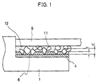
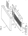
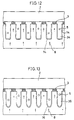
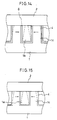
- Tête à jets d'encre destinée à une imprimante à jets d'encre ayant une chambre (1a) de pression formée par traitement par des fentes d'un matériau piézoélectrique pour la projection d'une encre, une électrode (4) de pilotage placée sur la chambre de pression (1a) et un film isolant (6) formé sur l'électrode de pilotage (4), une partie du film isolant (6) venant au contact de l'encre, caractérisée en ce que la connexion électrique entre l'électrode de pilotage (4) et une électrode extérieure (9) est réalisée par disposition de particules conductrices de l'électricité (11) dans le film isolant (6) à l'aide d'un élément (12) de liaison électrique contenant les particules conductrices de l'électricité (11).
- Tête à jets d'encre selon la revendication 1, dans laquelle l'élément de liaison électrique (12) contient des particules conductrices de l'électricité (11) ayant un diamètre particulaire supérieur à l'épaisseur du film isolant (6) et une dureté supérieure à celle du film isolant (6).
- Tête à jets d'encre selon la revendication 1 ou 2, dans laquelle le film isolant (6) est un film de polyparaxylylène.
- Tête à jets d'encre selon l'une quelconque des revendications 1 à 3, dans laquelle l'électrode de pilotage (4) est formée sur une partie de la paroi interne de la chambre de pression (1a) formée d'un matériau piézoélectrique.
- Tête à jets d'encre selon l'une quelconque des revendications 1 à 4, dans laquelle la chambre de pression (1a) formée par traitement par des fentes d'une base piézoélectrique (1) devient une fente de connexion de faible profondeur à la partie de liaison avec l'électrode externe (9).
- Tête à jets d'encre selon l'une quelconque des revendications 1 à 5, dans laquelle l'électrode externe (9) comporte une électrode (49) en forme de motif sur un film.
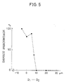
- Tête à jets d'encre selon la revendication 6, dans laquelle l'épaisseur de l'électrode (49) en forme de motif est supérieure à la profondeur d'une fente de connexion d'au moins 10 µm.
- Procédé de production d'une tête à jets d'encre destinée à une imprimante à jets d'encre ayant une chambre de pression (1a) formée par traitement des fentes d'un matériau piézoélectrique de projection d'une encre, une électrode de pilotage (4) placée sur la chambre de pression (1a) et un film isolant (6) formé sur l'électrode de pilotage (4), une partie du film isolant (6) venant au contact de l'encre, caractérisé en ce que des particules conductrices de l'électricité (11) passent à travers le film isolant (6) lors de la disposition d'un élément de liaison électrique (12) contenant des particules conductrices de l'électricité (11) de diamètre particulaire supérieur à l'épaisseur du film isolant (6) et de dureté supérieure à celle du film isolant (6), et l'exécution de la mise sous pression à un état de chauffage depuis la partie supérieure de l'électrode externe (9) pour l'exécution de la connexion électrique entre l'électrode de pilotage (4) et l'électrode externe (9).
Applications Claiming Priority (5)
| Application Number | Priority Date | Filing Date | Title |
|---|---|---|---|
| JP198935/92 | 1992-07-03 | ||
| JP19893592A JP3179195B2 (ja) | 1992-07-03 | 1992-07-03 | インクジェットヘッド |
| JP26785692A JP3132916B2 (ja) | 1992-09-11 | 1992-09-11 | インクジェットプリントヘッド |
| JP267856/92 | 1992-09-11 | ||
| PCT/JP1993/000921 WO1994001284A1 (fr) | 1992-07-03 | 1993-07-05 | Tete a jet d'encre |
Publications (3)
| Publication Number | Publication Date |
|---|---|
| EP0647525A1 EP0647525A1 (fr) | 1995-04-12 |
| EP0647525A4 EP0647525A4 (fr) | 1996-01-03 |
| EP0647525B1 true EP0647525B1 (fr) | 1998-09-30 |
Family
ID=26511257
Family Applications (1)
| Application Number | Title | Priority Date | Filing Date |
|---|---|---|---|
| EP93914954A Expired - Lifetime EP0647525B1 (fr) | 1992-07-03 | 1993-07-05 | Tete a jet d'encre |
Country Status (4)
| Country | Link |
|---|---|
| US (1) | US5719606A (fr) |
| EP (1) | EP0647525B1 (fr) |
| DE (1) | DE69321349T2 (fr) |
| WO (1) | WO1994001284A1 (fr) |
Families Citing this family (11)
| Publication number | Priority date | Publication date | Assignee | Title |
|---|---|---|---|---|
| CN1191936C (zh) * | 1996-04-23 | 2005-03-09 | 萨尔技术有限公司 | 液滴沉积装置及其制造方法 |
| US6808250B2 (en) | 1997-01-10 | 2004-10-26 | Konica Corporation | Production method of ink-jet head |
| JPH115303A (ja) * | 1997-06-18 | 1999-01-12 | Brother Ind Ltd | インクジェットプリンタヘッド |
| JP3123468B2 (ja) * | 1997-06-25 | 2001-01-09 | 日本電気株式会社 | インクジェット記録ヘッド及びその製造方法 |
| US6572221B1 (en) | 1997-10-10 | 2003-06-03 | Xaar Technology Limited | Droplet deposition apparatus for ink jet printhead |
| US6623865B1 (en) | 2000-03-04 | 2003-09-23 | Energenius, Inc. | Lead zirconate titanate dielectric thin film composites on metallic foils |
| JP3693118B2 (ja) * | 2002-08-12 | 2005-09-07 | セイコーエプソン株式会社 | シリコンデバイスの製造方法及び液体噴射ヘッドの製造方法並びに液体噴射ヘッド |
| US20040102022A1 (en) * | 2002-11-22 | 2004-05-27 | Tongbi Jiang | Methods of fabricating integrated circuitry |
| US20040175585A1 (en) * | 2003-03-05 | 2004-09-09 | Qin Zou | Barium strontium titanate containing multilayer structures on metal foils |
| JP5563354B2 (ja) * | 2010-04-01 | 2014-07-30 | エスアイアイ・プリンテック株式会社 | 液体噴射ヘッド及び液体噴射装置 |
| JP6301602B2 (ja) * | 2013-07-22 | 2018-03-28 | ローム株式会社 | パワーモジュールおよびその製造方法 |
Family Cites Families (21)
| Publication number | Priority date | Publication date | Assignee | Title |
|---|---|---|---|---|
| JPS5912828B2 (ja) * | 1976-07-19 | 1984-03-26 | 株式会社大林組 | 鉄筋コンクリ−ト構造骨組の柱・梁接合部 |
| US4216477A (en) * | 1978-05-10 | 1980-08-05 | Hitachi, Ltd. | Nozzle head of an ink-jet printing apparatus with built-in fluid diodes |
| US4568602A (en) * | 1983-01-24 | 1986-02-04 | Minnesota Mining And Manufacturing Company | Sheet material adapted to provide long-lived stable adhesive-bonded electrical connections |
| DE3306098A1 (de) * | 1983-02-22 | 1984-08-23 | Siemens AG, 1000 Berlin und 8000 München | Piezoelektrisch betriebener schreibkopf mit kanalmatrize |
| JPS6159914A (ja) * | 1984-08-31 | 1986-03-27 | Fujitsu Ltd | デイジタル圧縮装置 |
| US5045249A (en) * | 1986-12-04 | 1991-09-03 | At&T Bell Laboratories | Electrical interconnection by a composite medium |
| US4879568A (en) * | 1987-01-10 | 1989-11-07 | Am International, Inc. | Droplet deposition apparatus |
| JPS63249393A (ja) * | 1987-04-03 | 1988-10-17 | シャープ株式会社 | 電子部品の接続方法 |
| JPH01168859A (ja) * | 1987-12-23 | 1989-07-04 | Matsushita Electric Works Ltd | ポリパラキシリレンのコーティング方法 |
| US5197892A (en) * | 1988-05-31 | 1993-03-30 | Canon Kabushiki Kaisha | Electric circuit device having an electric connecting member and electric circuit components |
| GB8824014D0 (en) * | 1988-10-13 | 1988-11-23 | Am Int | High density multi-channel array electrically pulsed droplet deposition apparatus |
| JPH02208050A (ja) * | 1989-02-07 | 1990-08-17 | Ricoh Co Ltd | インクジェット記録装置の記録ヘッド及び振動子電圧印加方法 |
| JP2813428B2 (ja) * | 1989-08-17 | 1998-10-22 | 三菱電機株式会社 | 電界効果トランジスタ及び該電界効果トランジスタを用いた液晶表示装置 |
| ATE138225T1 (de) * | 1989-08-17 | 1996-06-15 | Canon Kk | Prozess zur gegenseitigen konnektion von elektrodenanschlüssen |
| JP3029129B2 (ja) * | 1990-02-13 | 2000-04-04 | キヤノン株式会社 | 記録ヘッド用導電シート及びこれを用いた記録ヘッド並びに記録装置 |
| US5099437A (en) * | 1990-10-09 | 1992-03-24 | Fugitive Emissions Control, Inc. | Emissions monitoring and tracking system |
| JP2935886B2 (ja) * | 1990-11-09 | 1999-08-16 | シチズン時計株式会社 | インクジェットヘッド |
| JPH04182133A (ja) * | 1990-11-16 | 1992-06-29 | Citizen Watch Co Ltd | 液滴噴射記録装置 |
| JPH04263955A (ja) * | 1991-02-19 | 1992-09-18 | Citizen Watch Co Ltd | インクジェットヘッドの製造方法 |
| JPH05196952A (ja) * | 1991-10-02 | 1993-08-06 | Canon Inc | 電気的接続構造及び電気的接続方法 |
| JP3077639B2 (ja) * | 1997-08-27 | 2000-08-14 | 日本電気株式会社 | 誤り訂正バランス符号送受信システム |
-
1993
- 1993-07-05 EP EP93914954A patent/EP0647525B1/fr not_active Expired - Lifetime
- 1993-07-05 US US08/367,138 patent/US5719606A/en not_active Expired - Fee Related
- 1993-07-05 WO PCT/JP1993/000921 patent/WO1994001284A1/fr active IP Right Grant
- 1993-07-05 DE DE69321349T patent/DE69321349T2/de not_active Expired - Fee Related
Also Published As
| Publication number | Publication date |
|---|---|
| DE69321349T2 (de) | 1999-02-25 |
| DE69321349D1 (de) | 1998-11-05 |
| EP0647525A1 (fr) | 1995-04-12 |
| US5719606A (en) | 1998-02-17 |
| EP0647525A4 (fr) | 1996-01-03 |
| WO1994001284A1 (fr) | 1994-01-20 |
Similar Documents
| Publication | Publication Date | Title |
|---|---|---|
| EP0511376B1 (fr) | Tete a jet d'encre a transducteur a couche mince | |
| US7478899B2 (en) | Piezoelectric ink jet module with seal | |
| KR100444641B1 (ko) | 반도체 장치 | |
| EP0647525B1 (fr) | Tete a jet d'encre | |
| KR100465444B1 (ko) | 협 피치용 커넥터, 정전 액추에이터, 압전 액추에이터,잉크 제트 헤드, 잉크 제트 프린터, 마이크로머신, 액정패널, 전자기기 | |
| US6345887B1 (en) | Ink jet head for non-impact printer | |
| JP2017124540A (ja) | 配線基板、memsデバイス及び液体噴射ヘッド | |
| JP2001130012A (ja) | インクジェットのダイ用の電気的相互接続 | |
| US7204586B2 (en) | Ink jet printing module | |
| US7525236B2 (en) | Piezoelectric element unit, manufacturing method of the same, and liquid ejecting head using the same | |
| US7290868B2 (en) | Inkjet head with formed external circuit connecting electrodes | |
| EP1548826B1 (fr) | Disposition de contacts de puces | |
| US20120026248A1 (en) | Inkjet head assembly and method for manufacturing the same | |
| JP3484675B2 (ja) | インク液噴射型プリンター用ヘッド実装構成体 | |
| JP6950313B2 (ja) | 液体噴射ヘッド及び液体噴射装置 | |
| JP3201004B2 (ja) | インクジェットヘッド | |
| JP2002254629A (ja) | インクジェットヘッド | |
| JP6891681B2 (ja) | 液体噴射ヘッド及び液体噴射装置 | |
| JP2010012724A (ja) | 液滴吐出ヘッド、画像形成装置、及び液滴吐出ヘッドの製造方法 | |
| JP3125326B2 (ja) | インクジェット記録装置 | |
| JP2006121045A (ja) | ボンディング構造、アクチュエータ装置及び液体噴射ヘッド | |
| JPH0781048A (ja) | インク噴射装置 | |
| KR100327247B1 (ko) | 플립칩 본딩법을 이용한 잉크젯 프린트 헤드와 전원 및 신호인가선의 연결방법 | |
| JP3672049B2 (ja) | インクジェットプリントヘッドの駆動素子の回路接続方法 | |
| JP2001260353A (ja) | インクジェットヘッド及びインクジェット記録装置 |
Legal Events
| Date | Code | Title | Description |
|---|---|---|---|
| PUAI | Public reference made under article 153(3) epc to a published international application that has entered the european phase |
Free format text: ORIGINAL CODE: 0009012 |
|
| 17P | Request for examination filed |
Effective date: 19950124 |
|
| AK | Designated contracting states |
Kind code of ref document: A1 Designated state(s): DE FR GB |
|
| RIN1 | Information on inventor provided before grant (corrected) |
Inventor name: HIRAISHI, HISATO Inventor name: NAGASHIMA, TAKAYUKI Inventor name: UGA, MASAYASU Inventor name: IKEDA, TOMOO Inventor name: KIGAWA, KEISUKE |
|
| A4 | Supplementary search report drawn up and despatched | ||
| AK | Designated contracting states |
Kind code of ref document: A4 Designated state(s): DE FR GB |
|
| 17Q | First examination report despatched |
Effective date: 19970110 |
|
| GRAG | Despatch of communication of intention to grant |
Free format text: ORIGINAL CODE: EPIDOS AGRA |
|
| GRAG | Despatch of communication of intention to grant |
Free format text: ORIGINAL CODE: EPIDOS AGRA |
|
| GRAH | Despatch of communication of intention to grant a patent |
Free format text: ORIGINAL CODE: EPIDOS IGRA |
|
| GRAH | Despatch of communication of intention to grant a patent |
Free format text: ORIGINAL CODE: EPIDOS IGRA |
|
| GRAA | (expected) grant |
Free format text: ORIGINAL CODE: 0009210 |
|
| AK | Designated contracting states |
Kind code of ref document: B1 Designated state(s): DE FR GB |
|
| REF | Corresponds to: |
Ref document number: 69321349 Country of ref document: DE Date of ref document: 19981105 |
|
| ET | Fr: translation filed | ||
| PLBE | No opposition filed within time limit |
Free format text: ORIGINAL CODE: 0009261 |
|
| STAA | Information on the status of an ep patent application or granted ep patent |
Free format text: STATUS: NO OPPOSITION FILED WITHIN TIME LIMIT |
|
| 26N | No opposition filed | ||
| REG | Reference to a national code |
Ref country code: GB Ref legal event code: IF02 |
|
| PGFP | Annual fee paid to national office [announced via postgrant information from national office to epo] |
Ref country code: GB Payment date: 20020703 Year of fee payment: 10 |
|
| PGFP | Annual fee paid to national office [announced via postgrant information from national office to epo] |
Ref country code: FR Payment date: 20020709 Year of fee payment: 10 |
|
| PGFP | Annual fee paid to national office [announced via postgrant information from national office to epo] |
Ref country code: DE Payment date: 20020710 Year of fee payment: 10 |
|
| PG25 | Lapsed in a contracting state [announced via postgrant information from national office to epo] |
Ref country code: GB Free format text: LAPSE BECAUSE OF NON-PAYMENT OF DUE FEES Effective date: 20030705 |
|
| PG25 | Lapsed in a contracting state [announced via postgrant information from national office to epo] |
Ref country code: DE Free format text: LAPSE BECAUSE OF NON-PAYMENT OF DUE FEES Effective date: 20040203 |
|
| GBPC | Gb: european patent ceased through non-payment of renewal fee |
Effective date: 20030705 |
|
| PG25 | Lapsed in a contracting state [announced via postgrant information from national office to epo] |
Ref country code: FR Free format text: LAPSE BECAUSE OF NON-PAYMENT OF DUE FEES Effective date: 20040331 |
|
| REG | Reference to a national code |
Ref country code: FR Ref legal event code: ST |