EP0647525B1 - Tintenstrahldruckkopf - Google Patents
Tintenstrahldruckkopf Download PDFInfo
- Publication number
- EP0647525B1 EP0647525B1 EP93914954A EP93914954A EP0647525B1 EP 0647525 B1 EP0647525 B1 EP 0647525B1 EP 93914954 A EP93914954 A EP 93914954A EP 93914954 A EP93914954 A EP 93914954A EP 0647525 B1 EP0647525 B1 EP 0647525B1
- Authority
- EP
- European Patent Office
- Prior art keywords
- insulating film
- ink jet
- ink
- pressure chamber
- electrode
- Prior art date
- Legal status (The legal status is an assumption and is not a legal conclusion. Google has not performed a legal analysis and makes no representation as to the accuracy of the status listed.)
- Expired - Lifetime
Links
Images


Classifications
-
- B—PERFORMING OPERATIONS; TRANSPORTING
- B41—PRINTING; LINING MACHINES; TYPEWRITERS; STAMPS
- B41J—TYPEWRITERS; SELECTIVE PRINTING MECHANISMS, i.e. MECHANISMS PRINTING OTHERWISE THAN FROM A FORME; CORRECTION OF TYPOGRAPHICAL ERRORS
- B41J2/00—Typewriters or selective printing mechanisms characterised by the printing or marking process for which they are designed
- B41J2/005—Typewriters or selective printing mechanisms characterised by the printing or marking process for which they are designed characterised by bringing liquid or particles selectively into contact with a printing material
- B41J2/01—Ink jet
- B41J2/135—Nozzles
- B41J2/14—Structure thereof only for on-demand ink jet heads
- B41J2/14201—Structure of print heads with piezoelectric elements
- B41J2/14209—Structure of print heads with piezoelectric elements of finger type, chamber walls consisting integrally of piezoelectric material
-
- B—PERFORMING OPERATIONS; TRANSPORTING
- B41—PRINTING; LINING MACHINES; TYPEWRITERS; STAMPS
- B41J—TYPEWRITERS; SELECTIVE PRINTING MECHANISMS, i.e. MECHANISMS PRINTING OTHERWISE THAN FROM A FORME; CORRECTION OF TYPOGRAPHICAL ERRORS
- B41J2/00—Typewriters or selective printing mechanisms characterised by the printing or marking process for which they are designed
- B41J2/005—Typewriters or selective printing mechanisms characterised by the printing or marking process for which they are designed characterised by bringing liquid or particles selectively into contact with a printing material
- B41J2/01—Ink jet
- B41J2/135—Nozzles
- B41J2/14—Structure thereof only for on-demand ink jet heads
- B41J2002/14379—Edge shooter
Definitions
- the present invention relates to an ink jet head of a drop-on-demand (DOD) type, and, more specifically, relates to an ink jet head of a piezoelectric type.
- DOD drop-on-demand
- ink jet printers of non-impact printers expanding the market that have a simple principle and are suitable also for color printing. It can be said that an ink jet printer of a so-called DOD type jetting ink drops only on formation of dots is the leading one of them.
- DOD type As typical examples of a DOD type can be mentioned a kaiser type disclosed in Japanese Patent Publication No. 12138/1978 and a thermal jet type disclosed in Japanese Patent Publication No. 59914/1986.
- a pressure chamber 1a is constituted by forming a slot on a piezoelectric base 1 and covering it with a flat-plate-like upper lid 2.
- a driving electrode 4 is provided on the inner wall of said slot 1 and voltage is applied onto a barrier 1c, a part of the above piezoelectric base 1 to deform said barrier 1c.
- the volume of the pressure chamber 1a is reduced by said deformation and ink supplied in the inside is pressurized, which jets ink drops from a nozzle hole provided in correspondence to said pressure chamber and performs printing.
- an electroconductive aqueous ink is used in an ink jet printer of a DOD type.
- EP-A-0 413 335 discloses a method of connecting electrodes whereby an insulating film covering one of the electrodes is formed with an opening to expose the surface of said electrode. The exposed portion is then provided with electroconductive particles which make the electrical connection between two sandwiched electrodes.
- Japanese Laid-Open Patent Publication No. 252750/1988 discloses a method of forming an electroconductive pattern on the upper surface of a piezoelectric base for wiring between a driving electrode and an IC (semiconductor integrated circuit) and from an IC to the outside.
- Japanese Laid-Open Patent Publication No. 182133/1992 discloses a method of providing a shallow connection slot at the end part extended from a slot of a pressure chamber and jointing an electrode in said connection slot and an electrode of a circuit base having a driving circuit with a copper foil wire.
- the driving electrode 4 performes a mounting treatment for performing connection with the above IC or a copper foil wire electrically somewhere (generally at the end part opposite to the ink jetting side). For this, the electroconductive surface of said driving electrode must be usually exposed at the place where said mounting treatment is performed.
- the insulating film 6 is formed so as to have a fully strong adhesion with the driving electrode 4 for preventing a short circuit caused by the permeation of ink, it is very difficult to perform a method of taking off said insulating film formed partially.
- the permeation of ink may easily occur on the interface of the insulating film and the driving electrode with the end part of the insulating film as a starting point, which, moreover, may lead to a problem of peeling on said interface.
- a copper foil wire cannot but be made an extremely weak and thin form on condition of about 100 ⁇ m pitch as described above, and there is a large possibility of deformation and breakage.
- the number of copper foil wires to be used for one head is from several tens to one hundred and several tens, and it requires great care and efforts to put all these copper foil wires into the above connection slot provided on the piezoelectric base without breakage to joint them.
- a conventional shearing mode type has the following problems on deformation of the pressure chamber.
- Fig. 19 is an analytic perspective view of an ink jet head employing a shearing mode and forms a lot of long and thin slots on a piezoelectric material 28 such as PZT (lead zirconate titanate) in parallel. And the upper surface parts of barriers 48ab and 48bc remaining among slots are bonded to a glass, ceramic or plastic lid 2 with an elastic component 3 softly.
- a piezoelectric material 28 such as PZT (lead zirconate titanate)
- the slots becomes pressure chambers 38a, 38b and 38c filled with ink.
- each of pressure chambers 38a, 38b and 38c can supply ink from a common ink reservoir (not shown), and a nozzle plate 7 with a small nozzle 5 is adhered to the other end.
- the piezoelectric material 28 including barriers 48ab and 48bc are polarized in one direction as shown by an arrow 8 (or in the reverse direction).
- Electrodes 18a, 18b and 18c are formed in, the internal surface of slots.
- Fig. 16 is a sectional construction view of an ink jet head employing the shearing mode on non-driving.
- the barrier 48ab causes deformation of a shearing mode according to the direct crossing of a line of electric force 58ab and the polarization direction of the piezoelectric material in the barrier as shown in Fig. 17.
- the sectional area of the pressure chamber 38b reduces from the initial condition of Fig. 16 to the condition of Fig. 17. Namely, if the pressure chamber 38b is filled with ink, the pressure of ink rises instantaneously by the reduction of the volume of the slot and ink drops are jetted from the nozzle.
- a line of electric force 68ab occurs by the leakage of an electric field to the barrier 48ab and the lower part of the pressure chamber 38a.
- a line of electric force 68bc occurs by the leakage of an electric field to the barrier 48bc and the lower part of the pressure chamber 38bc.
- lines of electric force 68ab and 68bc look to the same direction almost in parallel with the polarization direction of the piezoelectric material at the lower parts of the pressure chambers 38a and 38b, elongation deformation in the direction occurs and the bottom part of the pressure chamber 38b is lifted up as shown with a one-dot chain line.
- Such deformation is called a revolution.
- the piezoelectric material 28 is deformed as shown with a two-dot chain line when only the barrier 78a is driven to deform the surrounding barriers 78b and 78c different from the barrier 78a.
- the bottom part of the pressure chamber 38b rises to reduce the sectional area of a pressure chamber, and hence an effect of increasing the, above jetting power can be anticipated.
- the present inventors measured the amount of displacement of the barrier 78a according to laser measurement with a view to making the balance clear.
- a very small mirror is adhered onto the upper surface of a barrier, and altering voltage to be applied onto electrodes on both sides of the barrier, the moving amount of the mirror is measured according to laser light irradiated onto the mirror, which is converted into the amount of deformation of the barrier.
- the reduction of the jetting speed induces the instability of the jetting direction of ink drops, which not only causes the deviation of the position of printed dots but also makes it impossible to jet ink made highly viscous around the nozzle, which leads to a fatal defect of the dislocation of printed dots.
- an ink jet head having the features recited in Claim 1 and a method of producing a head comprising the features of Claim 8.
- an insulating film is formed on a driving electrode of a mounting treatment part in addition onto a driving electrode of a pressure chamber and left in the ink jet head of the present invention, and electric connection with an IC or an external electrode is performed with an electrical jointing component containing electroconductive particles with a higher hardness and a larger diameter than those of said insulating film.
- a particularly important effect is that the occurrence of various defects due to a short circuit between driving electrodes can be prevented even if undesirable conditions such as ink adhesion and moisure condensation occur at said mounting part, which can improve the reliability of a head.
- the circumference of the above electroconductive particles is also protected electrically with an adhesive insulating component constructing the above electrical jointing component, and no problem upon reliability at the part of said electroconductive particles occurs.
- the above difficulties in the process of removing an insulating film disappear, needless to say.
- the present invention employs a pattern electrode formed on a film according to the means dissolving the above first problem as an external electrode and performs mounting by fitting said pattern electrode to a connection slot provided on one end of the above piezoelectric base. It is characterized in that the thickness of the pattern electrode is larger than the depth of the above connection slot by more than 10 ⁇ m.
- connection slot and a pattern electrode By mounting a connection slot and a pattern electrode according to fitting construction, various advantages upon reliability and a yield as below can be fulfilled:
- Fig. 1 is a side view of a mounting treatment part of a first ink jet head according to the present invention
- Fig. 2 is an analytic perspective view thereof.
- Fig. 3 is an analytic perspective view of a mounting treatment part of a second ink jet head according to the present invention
- Fig. 4 is a sectional view of the mounting treatment part
- Fig. 5 is an explanatory view for its characteristics.
- Figs. 6-8 show a pressure chamber of an ink jet head; Fig. 6 is a sectional view on non-driving, Fig. 7 is a sectional view on driving, and Fig. 8 is an enlarged view of a part of a barrier.
- Figs. 9-11 show a pressure chamber of an ink jet head; Fig. 9 is a sectional view on non-driving, Fig. 10 is a sectional view on driving, and Fig. 11 is an enlarged view of a part of a barrier.
- Fig. 12 is a sectional view on non-driving of an ink jet head.
- Fig. 13 is a sectional view on non-driving of an ink jet head.
- Fig. 14 is a sectional view of a pressure chamber of an ink jet head of a conventional shearing mode.
- Fig. 15 is a sectional view of a pressure chamber of an ink jet head of a conventional shearing mode having no insulating film and Figs. 16-19 show a conventional ink jet head employing a shearing mode;
- Fig. 16 is a sectional structural view on non-driving,
- Fig. 17 is a sectional view on driving,
- Fig. 18 shows the condition of the deformation of barriers of a piezoelectric material and its surrounding barriers on driving, and
- Fig. 19 is an analytic perspective view.
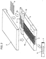
- Fig. 2 is an analytic perspective view of an ink jet head according to the present invention.
- a sheet-like piezoelectric base 1 has a first slot with a rectangular sectional form becoming a pressure chamber 1a and a second slot crossing with said slot and becoming an ink supply path 10 for supplying ink into said slot, and a driving electrode 4 is formed on the inner wall of said first slot.
- the driving electrode 4 extends to the tip of the ink supply path 10 to become a shallow connection slot 35 at the rear end part (B part) of the head and is mount-connected with an external electrode 9 here.
- An upper lid 2 is adhered to make the above first slot a pressure chamber 1a, and a nozzle plate 7 is secured to the front end part of the head so that a nozzle hole 5 is provided in correspondence to said pressure chamber.
- Ink introduced into the thus prepared head through the ink supply path 10 is jetted from the nozzle hole 5 as ink drops by changing the pressure of the pressure chamber 1a in correspondence to a signal from the external electrode 9.
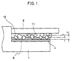
- Fig. 1 is an enlarged view of the rear end part (B part) of a head of Fig. 2, a side view for explaining the present invention in detail.
- an insulating film 6 is formed on the driving electrode 4, and further the external electrode 9 is jointed mechanically and electrically with an electrical jointing component containing electroconductive particles 11.
- a gold film with a thickness of 0.3 ⁇ m is formed on the piezoelectric base 1 of PZT (lead zirconate titanate) as the driving electrode 4 according to spattering. Subsequently, poly-para-xylylene with a thickness of 5 ⁇ m is formed as the insulating film 6 according to chemical metallizing.
- PZT lead zirconate titanate
- Poly-para-xylylene is a soft film with a Rockwell hardness of R80 (ASTM-D-785) and a pencil hardness of H.
- the external electrode 9 formed of gold-plated copper foil and the driving electrode 4 are jointed electrically with an electrical jointing component 12 containing electroconductive particles 11 with an average particle diameter of 7 ⁇ m.
- Said jointing component has an epoxy resin as the aggregate and Ni particles of a hard metal dispersed therein as electroconductive particles 11.
- the above aggregate is cured according to heat contact bonding from the top of the external electrode 9 to accomplish mechanical linking, and hard electroconductive particles 11 break the insulating film 6 very soft in comparison with them on pressurizing to accomplish electrical jointing.
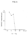
- the reliability of electrical jointing was examined by determining the average particle diameter of electroconductive particles 11 to 7 ⁇ m and changing the thickness of a poly-para-xylene film.
- the driving electrode 4 and the external electrode 9 are electrically connected since electroconductive particles break through the insulating film 6 and pop out at both sides of the insulating film.
- said insulating film has a thickness of 1 ⁇ m or more, preferably 3 ⁇ m or more, and inevitably that d is 1 ⁇ m or more, preferably 3 ⁇ m or more.
- high polymeric, relatively soft insulating films can be also mentioned a polyimide resin, a polyamide resin, a polyester resin and a silicone resin according to coating and polyethylene and polystyrene according to plasma polymerization.
- the percentage of defects corresponding to Table 1 was 5 % and it was revealed that Ni particles might fail to break through an insulating film sufficiently in some cases.
- Fig. 3 is a perspective view showing another embodiment of the present invention, a part corresponding to the B part of Fig. 2.
- a slot extending from a pressure chamber 1a is treated to be a shallow connection slot 35 at the back end part of a piezoelectric base 1, and a driving electrode 4 and an insulating film 6 thereupon are formed in said connection slot 35.
- the portion is similar to that of Fig. 2.
- an external electrode has a pattern electrode 49 on a film 39, which is flexible wiring.
- Fig. 4 is an enlarged sectional view of an ink jet head shown in Fig. 3 around the connection slot.
- the pattern electrode 49 is mounted in a fitting manner with the connection slot 35, and, as described above, said electrode and driving electrode 4 can be connected electrically with electroconductive particles 11.
- press heating is performed in one lot with a hot tool from the top of the film 39.
- the space between the part without the above pattern electrode on the lower surface of the film 39 and the surface of the piezoelectric base is filled with said jointing component and cured. Because of it, mechanical jointing strength between a film with said pattern electrode and the piezoelectric base 1 is enhanced sharply.
- the electrical jointing component 12 containing electroconductive particles 11 is a so-called anisotropic electroconductive component capable of obtaining electroconductivity in a direction of thickness but expressing insulating properties in a planar direction; according to the constitution of the present invention, however, the performance of expressing insulating properties in said planar direction is improved even in case of a minute pitch since adjacent electrodes are separated according to the three-dimensional form of slots.
- the transverse axis shows values of D1-D2 according to various constitutions and the vertical axis shows percentages of conductive defects.
- the measurement of said conductive defects was performed in the same manner as in Table 1.
- Fig. 6 corresponds to Fig. 16 of a conventional example.
- pressure chambers 30a, 30b and 30c related to ink jetting correspond to pressure chambers 38a, 38b and 38c of Fig. 16 respectively, and similarly to Fig. 16, a nozzle 5 is provided at the end part of each pressure chamber.
- a concave part 70 is provided at the bottom part of pressure chambers 30a, 30b and 30c.
- the sectional form of the concave part 70 at the bottom part of a pressure chamber is formed of at least two lines combined; particularly both lines are linear, and the right and the left have almost symmetric forms.
- electrodes 4a, 4b and 4c are formed in the internal surfaces of pressure chambers.
- Fig. 7 is an explanatory view for the effect of the present embodiment, corresponding to Fig. 17 of a conventional example.
- the line of electric force 50ab in the barrier 40ab is formed so that it crosses with the polarization direction of a piezoelectric material, and the barrier 40bc causes the deformation of a shearing mode similarly to the case of Fig. 17.
- the sectional area (volume of the flow path of the pressure chamber 30b) of the pressure chamber 30b related to ink jetting reduces according to the deformation of a shearing mode of barriers 40ab and 40bc to cause ink to jet out of the nozzle 5.
- the line of electric force caused by a leakage electric field becomes a curve from a slope at the right side of the bottom part of the pressure chamber 30a (side having a certain direction not right-angled to the polarization direction of a piezoelectric material) to a slope at the left side of the bottom part Of the pressure chamber 30b like lines of electric force 60ab and 60bc.
- the direction of the end point of the line of electric force 60ab shown in Fig. 7 is expressed as the direction vector A.
- the direction vector A can be divided into two directional components of the vector X and the vector Y.
- the vector X is a vector component in a direction of crossing with the polarization direction of a piezoelectric material.
- the vector X functions purely in a direction helping a shearing mode.
- the vector Y is a vector component in parallel with the polarization direction of a piezoelectric material. Because of it, the vector Y functions in a direction inducing a revolution.
- the length of a line of electric force produced by the left half of the electrode 4a and the electrode 4b becomes very long and can be disregarded compared with an influence by the right half of the electrode 4a.
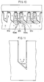
- Fig. 9 corresponds to Fig. 16 of a conventional example and shows another embodiment of an ink jet head.
- pressure chambers 32a, 32b and 32c related to ink jetting correspond to ink chambers 38a, 38b and 38c of Fig. 16 respectively, and similarly to Fig. 16, a nozzle 5 is provided at the end part of each pressure chamber.
- a concave part 72 is provided at the bottom parts of ink chambers 31a, 32b and 32c.
- the sectional form of the concave part 72 at the bottom part of a pressure chamber is composed of one slant straight line and hence it is non-symmetric.
- Fig. 10 is an explanatory view for the function of the present embodiment, corresponding to Fig. 17 of a conventional example.
- a line of electric force caused by a leakage electrid field becomes a curve from a side almost right-angled to the polarization direction of a piezoelectric material to a side with a certain angle (or in reverse) like lines of electric force 62ab and 62bc.
- the vector at the end point of the line of electric force 62ab shown in Fig. 10 is expressed as the direction vector B (Fig. 11).
- the direction vector B can be divided into two directional components of the vector U and the vector V.
- the vector U is a vector component in a direction of crossing with the polarization direction of a piezoelectric material. Because of it, the vector U functions purely in a direction helping a shearing mode.
- the vector V is a vector component in parallel with the polarization direction of a piezoelectric material. Because of it, the vector V functions in a direction inducing a revolution.
- Fig. 12 corresponds to Fig. 16 of a conventional example and shows the constitution of another embodiment related to a pressure chamber of an ink jet head.
- an ink chamber 34 related to ink jetting corresponds to ink chambers 38a, 38b and 38c of Fig. 16, and similarly to Fig. 16, a nozzle 5 is provided at the end part of each ink chamber.
- a concave part 74 is provided at the bottom part of the pressure chamber 34.
- the concave form of the concave part 74 at the bottom part of a pressure chamber is composed of a segment combined with at least two lines, which is mentioned as an example of an embodiment having a form composed of two curved sides and one straight line.
- a leakage electric field at the curved part of the bottom part of an ink chamber causes a revolution function slowly as it turns to the bottom part of the pressure chamber 34, which has another effect of causing deformation of a smooth shearing mode since the point of a deformation function purely of a shearing mode comes upward in the concave part of the bottom part of a pressure chamber.
- Fig. 13 corresponds to Fig. 16 of a conventional example and shows another embodiment related to a pressure chamber of an ink jet head.
- a pressure chamber 36 related to ink jetting corresponds to ink chambers 38a, 38b and 38c of Fig. 16, and similarly to Fig. 16, a nozzle 5 is provided at the end part of each pressure chamber.
- a concave part 76 is provided at the bottom part of the pressure chamber 36.
- the concave form of the concave part 76 at the bottom part of a slot is formed of a line combined with one curve.
- Embodiment 5 Only one difference from Embodiment 5 is that the present embodiment contains no straight line, and the same effect as in Embodiment 3 can be obtained.
- electrical connection can be accomplished in a state of forming an insulating film on an electrode at the side of an ink jet head in the mounting treatment part with an external electrode.
- the sectional form of the bottom part of a slot becoming an ink chamber and pressure chamber is composed of a segment containing a slope not vertical to a polarization direction.
- the bottom part of an ink chamber has a concave part, and one of the concave forms at the concave part of the bottom part is composed of at least two lines, one is composed of one slant straight line and one is composed of one curve.
- the line of electric force can be divided into a vertical direction component to a polarization direction and a component in parallel therewith, and the vertical direction component causes deformation purely of a shearing mode and the parallel direction component induces a revolution.
- the deterioration of ink jetting power reduces to dissolve the decrease of a jetting speed of ink drops, and further ink made highly viscous around a nozzle can also be jetted.
Claims (8)
- Tintenstrahlkopf für einen Tintenstrahldrucker, der eine Druckkammer (1a) besitzt, die gebildet wurde durch Schlitzbearbeiten eines piezoelektrischen Materials zum Ausstoßen von Tinte, eine Antriebselektrode (4), angebracht auf der Druckkammer (1a), und eine Isolierschicht (6), ausgebildet auf der Antriebselektrode (4), wobei ein Teil dieser Isolierschicht (6) mit der Tinte in Berührung kommt, dadurch gekennzeichnet, dass eine elektrische Verbindung zwischen der Antriebselektrode (4) und einer externen Elektrode (9) hergestellt wird, indem elektrisch leitende Teilchen (11) durch die Isolierschicht (6) geleitet werden durch ein elektrisches Verbindungsteil (12), das die elektrisch leitenden Teilchen (11) enthält.
- Tintenstrahlkopf nach Anspruch 1, wobei das elektrische Verbindungsteil (12) elektrisch leitende Teilchen (11) enthält, deren Teilchendurchmesser größer ist als die Dicke der Isolierschicht (6) und die eine größere Härte besitzen als die Isolierschicht (6).
- Tintenstrahlkopf nach Anspruch 1 oder 2, wobei die Isolierschicht (6) eine Polyparaxylylenschicht ist.
- Tintenstrahlkopf nach einem der Ansprüche 1 bis 3, wobei die Antriebselektrode (4) auf einem Abschnitt der Innenwand der Druckkammer (1a), gebildet aus aus piezoelektrischem Material, angebracht ist.
- Tintenstrahlkopf nach einem der Ansprüche 1 bis 4, wobei die Druckkammer (1a), gebildet durch Schlitzbearbeiten einer piezoelektrischen Grundfläche (1), zu einem Verbindungsschlitz wird mit einer geringen Tiefe am Verbindungsstück zur externen Elektrode (9).
- Tintenstrahlkopf nach einem der Ansprüche 1 bis 5, wobei die externe Elektrode (9) auf einer Schicht eine Musterelektrode (49) aufweist.
- Tintenstrahlkopf nach Anspruch 6, wobei die Musterelektrode (49) 10 µm oder mehr dicker ist als ein Verbindugsschlitz tief ist.
- Verfahren zur Herstellung eines Tintenstrahlkopfes für einen Tintenstrahldrucker, umfassend eine Druckkammer (1a), gebildet durch Schlitzbearbeiten eines piezoelektrischen Materials zum Ausstoßen von Tinte, eine Antriebselektrode (4), die auf der Druckkammer (1a) angebracht ist, und eine Isolierschicht (6), die mit der Tinte in Berührung kommt, dadurch gekennzeichnet, dass elektrisch leitende Teilchen (11) durch die Isolierschicht (6) gehen, indem ein elektrisches Verbindungsteil (12), das elektrisch leitende Teilchen (11) enthält mit einem Teilchendurchmesser, der größer ist als die Dicke der Isolierschicht (6), und einer Härte, die größer ist als die der Isolierschicht (6), bereitgestellt wird, und durch unter Druck setzen im erwärmten Zustand vom Kopf der externen Elektrode (9) her, so dass eine elektrische Verbindung zwischen der Antriebselektrode (4) und der externen Elektrode (9) erfolgt.
Applications Claiming Priority (5)
| Application Number | Priority Date | Filing Date | Title |
|---|---|---|---|
| JP19893592A JP3179195B2 (ja) | 1992-07-03 | 1992-07-03 | インクジェットヘッド |
| JP198935/92 | 1992-07-03 | ||
| JP26785692A JP3132916B2 (ja) | 1992-09-11 | 1992-09-11 | インクジェットプリントヘッド |
| JP267856/92 | 1992-09-11 | ||
| PCT/JP1993/000921 WO1994001284A1 (en) | 1992-07-03 | 1993-07-05 | Ink jet head |
Publications (3)
| Publication Number | Publication Date |
|---|---|
| EP0647525A1 EP0647525A1 (de) | 1995-04-12 |
| EP0647525A4 EP0647525A4 (de) | 1996-01-03 |
| EP0647525B1 true EP0647525B1 (de) | 1998-09-30 |
Family
ID=26511257
Family Applications (1)
| Application Number | Title | Priority Date | Filing Date |
|---|---|---|---|
| EP93914954A Expired - Lifetime EP0647525B1 (de) | 1992-07-03 | 1993-07-05 | Tintenstrahldruckkopf |
Country Status (4)
| Country | Link |
|---|---|
| US (1) | US5719606A (de) |
| EP (1) | EP0647525B1 (de) |
| DE (1) | DE69321349T2 (de) |
| WO (1) | WO1994001284A1 (de) |
Families Citing this family (11)
| Publication number | Priority date | Publication date | Assignee | Title |
|---|---|---|---|---|
| JP3177897B2 (ja) * | 1996-04-23 | 2001-06-18 | ザール テクノロジー リミテッド | 液滴デポジット装置 |
| US6808250B2 (en) * | 1997-01-10 | 2004-10-26 | Konica Corporation | Production method of ink-jet head |
| JPH115303A (ja) * | 1997-06-18 | 1999-01-12 | Brother Ind Ltd | インクジェットプリンタヘッド |
| JP3123468B2 (ja) * | 1997-06-25 | 2001-01-09 | 日本電気株式会社 | インクジェット記録ヘッド及びその製造方法 |
| US6572221B1 (en) | 1997-10-10 | 2003-06-03 | Xaar Technology Limited | Droplet deposition apparatus for ink jet printhead |
| US6623865B1 (en) | 2000-03-04 | 2003-09-23 | Energenius, Inc. | Lead zirconate titanate dielectric thin film composites on metallic foils |
| JP3693118B2 (ja) * | 2002-08-12 | 2005-09-07 | セイコーエプソン株式会社 | シリコンデバイスの製造方法及び液体噴射ヘッドの製造方法並びに液体噴射ヘッド |
| US20040102022A1 (en) * | 2002-11-22 | 2004-05-27 | Tongbi Jiang | Methods of fabricating integrated circuitry |
| US20040175585A1 (en) * | 2003-03-05 | 2004-09-09 | Qin Zou | Barium strontium titanate containing multilayer structures on metal foils |
| JP5563354B2 (ja) | 2010-04-01 | 2014-07-30 | エスアイアイ・プリンテック株式会社 | 液体噴射ヘッド及び液体噴射装置 |
| JP6301602B2 (ja) * | 2013-07-22 | 2018-03-28 | ローム株式会社 | パワーモジュールおよびその製造方法 |
Family Cites Families (21)
| Publication number | Priority date | Publication date | Assignee | Title |
|---|---|---|---|---|
| JPS5912828B2 (ja) * | 1976-07-19 | 1984-03-26 | 株式会社大林組 | 鉄筋コンクリ−ト構造骨組の柱・梁接合部 |
| US4216477A (en) * | 1978-05-10 | 1980-08-05 | Hitachi, Ltd. | Nozzle head of an ink-jet printing apparatus with built-in fluid diodes |
| US4568602A (en) * | 1983-01-24 | 1986-02-04 | Minnesota Mining And Manufacturing Company | Sheet material adapted to provide long-lived stable adhesive-bonded electrical connections |
| DE3306098A1 (de) * | 1983-02-22 | 1984-08-23 | Siemens AG, 1000 Berlin und 8000 München | Piezoelektrisch betriebener schreibkopf mit kanalmatrize |
| JPS6159914A (ja) * | 1984-08-31 | 1986-03-27 | Fujitsu Ltd | デイジタル圧縮装置 |
| US5045249A (en) * | 1986-12-04 | 1991-09-03 | At&T Bell Laboratories | Electrical interconnection by a composite medium |
| US4887100A (en) * | 1987-01-10 | 1989-12-12 | Am International, Inc. | Droplet deposition apparatus |
| JPS63249393A (ja) * | 1987-04-03 | 1988-10-17 | シャープ株式会社 | 電子部品の接続方法 |
| JPH01168859A (ja) * | 1987-12-23 | 1989-07-04 | Matsushita Electric Works Ltd | ポリパラキシリレンのコーティング方法 |
| US5197892A (en) * | 1988-05-31 | 1993-03-30 | Canon Kabushiki Kaisha | Electric circuit device having an electric connecting member and electric circuit components |
| GB8824014D0 (en) * | 1988-10-13 | 1988-11-23 | Am Int | High density multi-channel array electrically pulsed droplet deposition apparatus |
| JPH02208050A (ja) * | 1989-02-07 | 1990-08-17 | Ricoh Co Ltd | インクジェット記録装置の記録ヘッド及び振動子電圧印加方法 |
| JP2813428B2 (ja) * | 1989-08-17 | 1998-10-22 | 三菱電機株式会社 | 電界効果トランジスタ及び該電界効果トランジスタを用いた液晶表示装置 |
| DE69026992T2 (de) * | 1989-08-17 | 1996-10-24 | Canon Kk | Prozess zur gegenseitigen Konnektion von Elektrodenanschlüssen |
| JP3029129B2 (ja) * | 1990-02-13 | 2000-04-04 | キヤノン株式会社 | 記録ヘッド用導電シート及びこれを用いた記録ヘッド並びに記録装置 |
| US5099437A (en) * | 1990-10-09 | 1992-03-24 | Fugitive Emissions Control, Inc. | Emissions monitoring and tracking system |
| JP2935886B2 (ja) * | 1990-11-09 | 1999-08-16 | シチズン時計株式会社 | インクジェットヘッド |
| JPH04182133A (ja) * | 1990-11-16 | 1992-06-29 | Citizen Watch Co Ltd | 液滴噴射記録装置 |
| JPH04263955A (ja) * | 1991-02-19 | 1992-09-18 | Citizen Watch Co Ltd | インクジェットヘッドの製造方法 |
| JPH05196952A (ja) * | 1991-10-02 | 1993-08-06 | Canon Inc | 電気的接続構造及び電気的接続方法 |
| JP3077639B2 (ja) * | 1997-08-27 | 2000-08-14 | 日本電気株式会社 | 誤り訂正バランス符号送受信システム |
-
1993
- 1993-07-05 US US08/367,138 patent/US5719606A/en not_active Expired - Fee Related
- 1993-07-05 EP EP93914954A patent/EP0647525B1/de not_active Expired - Lifetime
- 1993-07-05 DE DE69321349T patent/DE69321349T2/de not_active Expired - Fee Related
- 1993-07-05 WO PCT/JP1993/000921 patent/WO1994001284A1/ja active IP Right Grant
Also Published As
| Publication number | Publication date |
|---|---|
| DE69321349D1 (de) | 1998-11-05 |
| WO1994001284A1 (en) | 1994-01-20 |
| EP0647525A4 (de) | 1996-01-03 |
| DE69321349T2 (de) | 1999-02-25 |
| US5719606A (en) | 1998-02-17 |
| EP0647525A1 (de) | 1995-04-12 |
Similar Documents
| Publication | Publication Date | Title |
|---|---|---|
| US8491100B2 (en) | Piezoelectric ink jet module with seal | |
| EP0511376B1 (de) | Tintenstrahlkopf mit dünnschichtwandler | |
| EP0647525B1 (de) | Tintenstrahldruckkopf | |
| KR100465444B1 (ko) | 협 피치용 커넥터, 정전 액추에이터, 압전 액추에이터,잉크 제트 헤드, 잉크 제트 프린터, 마이크로머신, 액정패널, 전자기기 | |
| US6345887B1 (en) | Ink jet head for non-impact printer | |
| KR20030042044A (ko) | 좁은 피치용 커넥터, 정전 엑추에이터, 압전 엑추에이터,잉크 젯 헤드, 잉크 젯 프린터, 마이크로 머신, 액정 패널및 전자기기 | |
| JP2017124540A (ja) | 配線基板、memsデバイス及び液体噴射ヘッド | |
| JP2001130012A (ja) | インクジェットのダイ用の電気的相互接続 | |
| US7204586B2 (en) | Ink jet printing module | |
| JP4385653B2 (ja) | 液体噴射ヘッド及びその製造方法 | |
| US7525236B2 (en) | Piezoelectric element unit, manufacturing method of the same, and liquid ejecting head using the same | |
| US7290868B2 (en) | Inkjet head with formed external circuit connecting electrodes | |
| EP1548826B1 (de) | Chipkontaktlayout | |
| US20120026248A1 (en) | Inkjet head assembly and method for manufacturing the same | |
| JP3484675B2 (ja) | インク液噴射型プリンター用ヘッド実装構成体 | |
| JP6950313B2 (ja) | 液体噴射ヘッド及び液体噴射装置 | |
| JP3201004B2 (ja) | インクジェットヘッド | |
| JP2002254629A (ja) | インクジェットヘッド | |
| JP6891681B2 (ja) | 液体噴射ヘッド及び液体噴射装置 | |
| JP2010012724A (ja) | 液滴吐出ヘッド、画像形成装置、及び液滴吐出ヘッドの製造方法 | |
| JP3125326B2 (ja) | インクジェット記録装置 | |
| JP2006121045A (ja) | ボンディング構造、アクチュエータ装置及び液体噴射ヘッド | |
| JPH0781048A (ja) | インク噴射装置 | |
| KR100327247B1 (ko) | 플립칩 본딩법을 이용한 잉크젯 프린트 헤드와 전원 및 신호인가선의 연결방법 | |
| JP3672049B2 (ja) | インクジェットプリントヘッドの駆動素子の回路接続方法 |
Legal Events
| Date | Code | Title | Description |
|---|---|---|---|
| PUAI | Public reference made under article 153(3) epc to a published international application that has entered the european phase |
Free format text: ORIGINAL CODE: 0009012 |
|
| 17P | Request for examination filed |
Effective date: 19950124 |
|
| AK | Designated contracting states |
Kind code of ref document: A1 Designated state(s): DE FR GB |
|
| RIN1 | Information on inventor provided before grant (corrected) |
Inventor name: HIRAISHI, HISATO Inventor name: NAGASHIMA, TAKAYUKI Inventor name: UGA, MASAYASU Inventor name: IKEDA, TOMOO Inventor name: KIGAWA, KEISUKE |
|
| A4 | Supplementary search report drawn up and despatched | ||
| AK | Designated contracting states |
Kind code of ref document: A4 Designated state(s): DE FR GB |
|
| 17Q | First examination report despatched |
Effective date: 19970110 |
|
| GRAG | Despatch of communication of intention to grant |
Free format text: ORIGINAL CODE: EPIDOS AGRA |
|
| GRAG | Despatch of communication of intention to grant |
Free format text: ORIGINAL CODE: EPIDOS AGRA |
|
| GRAH | Despatch of communication of intention to grant a patent |
Free format text: ORIGINAL CODE: EPIDOS IGRA |
|
| GRAH | Despatch of communication of intention to grant a patent |
Free format text: ORIGINAL CODE: EPIDOS IGRA |
|
| GRAA | (expected) grant |
Free format text: ORIGINAL CODE: 0009210 |
|
| AK | Designated contracting states |
Kind code of ref document: B1 Designated state(s): DE FR GB |
|
| REF | Corresponds to: |
Ref document number: 69321349 Country of ref document: DE Date of ref document: 19981105 |
|
| ET | Fr: translation filed | ||
| PLBE | No opposition filed within time limit |
Free format text: ORIGINAL CODE: 0009261 |
|
| STAA | Information on the status of an ep patent application or granted ep patent |
Free format text: STATUS: NO OPPOSITION FILED WITHIN TIME LIMIT |
|
| 26N | No opposition filed | ||
| REG | Reference to a national code |
Ref country code: GB Ref legal event code: IF02 |
|
| PGFP | Annual fee paid to national office [announced via postgrant information from national office to epo] |
Ref country code: GB Payment date: 20020703 Year of fee payment: 10 |
|
| PGFP | Annual fee paid to national office [announced via postgrant information from national office to epo] |
Ref country code: FR Payment date: 20020709 Year of fee payment: 10 |
|
| PGFP | Annual fee paid to national office [announced via postgrant information from national office to epo] |
Ref country code: DE Payment date: 20020710 Year of fee payment: 10 |
|
| PG25 | Lapsed in a contracting state [announced via postgrant information from national office to epo] |
Ref country code: GB Free format text: LAPSE BECAUSE OF NON-PAYMENT OF DUE FEES Effective date: 20030705 |
|
| PG25 | Lapsed in a contracting state [announced via postgrant information from national office to epo] |
Ref country code: DE Free format text: LAPSE BECAUSE OF NON-PAYMENT OF DUE FEES Effective date: 20040203 |
|
| GBPC | Gb: european patent ceased through non-payment of renewal fee |
Effective date: 20030705 |
|
| PG25 | Lapsed in a contracting state [announced via postgrant information from national office to epo] |
Ref country code: FR Free format text: LAPSE BECAUSE OF NON-PAYMENT OF DUE FEES Effective date: 20040331 |
|
| REG | Reference to a national code |
Ref country code: FR Ref legal event code: ST |