EP0646895A2 - Carte à puce mince et méthode de sa fabrication - Google Patents
Carte à puce mince et méthode de sa fabrication Download PDFInfo
- Publication number
- EP0646895A2 EP0646895A2 EP94304992A EP94304992A EP0646895A2 EP 0646895 A2 EP0646895 A2 EP 0646895A2 EP 94304992 A EP94304992 A EP 94304992A EP 94304992 A EP94304992 A EP 94304992A EP 0646895 A2 EP0646895 A2 EP 0646895A2
- Authority
- EP
- European Patent Office
- Prior art keywords
- card
- module
- plate type
- thin
- support
- Prior art date
- Legal status (The legal status is an assumption and is not a legal conclusion. Google has not performed a legal analysis and makes no representation as to the accuracy of the status listed.)
- Granted
Links
Images


Classifications
-
- G—PHYSICS
- G06—COMPUTING; CALCULATING OR COUNTING
- G06K—GRAPHICAL DATA READING; PRESENTATION OF DATA; RECORD CARRIERS; HANDLING RECORD CARRIERS
- G06K19/00—Record carriers for use with machines and with at least a part designed to carry digital markings
- G06K19/06—Record carriers for use with machines and with at least a part designed to carry digital markings characterised by the kind of the digital marking, e.g. shape, nature, code
- G06K19/067—Record carriers with conductive marks, printed circuits or semiconductor circuit elements, e.g. credit or identity cards also with resonating or responding marks without active components
- G06K19/07—Record carriers with conductive marks, printed circuits or semiconductor circuit elements, e.g. credit or identity cards also with resonating or responding marks without active components with integrated circuit chips
- G06K19/077—Constructional details, e.g. mounting of circuits in the carrier
- G06K19/07749—Constructional details, e.g. mounting of circuits in the carrier the record carrier being capable of non-contact communication, e.g. constructional details of the antenna of a non-contact smart card
- G06K19/07766—Constructional details, e.g. mounting of circuits in the carrier the record carrier being capable of non-contact communication, e.g. constructional details of the antenna of a non-contact smart card comprising at least a second communication arrangement in addition to a first non-contact communication arrangement
- G06K19/07769—Constructional details, e.g. mounting of circuits in the carrier the record carrier being capable of non-contact communication, e.g. constructional details of the antenna of a non-contact smart card comprising at least a second communication arrangement in addition to a first non-contact communication arrangement the further communication means being a galvanic interface, e.g. hybrid or mixed smart cards having a contact and a non-contact interface
-
- G—PHYSICS
- G06—COMPUTING; CALCULATING OR COUNTING
- G06K—GRAPHICAL DATA READING; PRESENTATION OF DATA; RECORD CARRIERS; HANDLING RECORD CARRIERS
- G06K19/00—Record carriers for use with machines and with at least a part designed to carry digital markings
- G06K19/06—Record carriers for use with machines and with at least a part designed to carry digital markings characterised by the kind of the digital marking, e.g. shape, nature, code
- G06K19/067—Record carriers with conductive marks, printed circuits or semiconductor circuit elements, e.g. credit or identity cards also with resonating or responding marks without active components
- G06K19/07—Record carriers with conductive marks, printed circuits or semiconductor circuit elements, e.g. credit or identity cards also with resonating or responding marks without active components with integrated circuit chips
- G06K19/077—Constructional details, e.g. mounting of circuits in the carrier
- G06K19/07745—Mounting details of integrated circuit chips
-
- G—PHYSICS
- G06—COMPUTING; CALCULATING OR COUNTING
- G06K—GRAPHICAL DATA READING; PRESENTATION OF DATA; RECORD CARRIERS; HANDLING RECORD CARRIERS
- G06K19/00—Record carriers for use with machines and with at least a part designed to carry digital markings
- G06K19/06—Record carriers for use with machines and with at least a part designed to carry digital markings characterised by the kind of the digital marking, e.g. shape, nature, code
- G06K19/067—Record carriers with conductive marks, printed circuits or semiconductor circuit elements, e.g. credit or identity cards also with resonating or responding marks without active components
- G06K19/07—Record carriers with conductive marks, printed circuits or semiconductor circuit elements, e.g. credit or identity cards also with resonating or responding marks without active components with integrated circuit chips
- G06K19/077—Constructional details, e.g. mounting of circuits in the carrier
- G06K19/07749—Constructional details, e.g. mounting of circuits in the carrier the record carrier being capable of non-contact communication, e.g. constructional details of the antenna of a non-contact smart card
- G06K19/0775—Constructional details, e.g. mounting of circuits in the carrier the record carrier being capable of non-contact communication, e.g. constructional details of the antenna of a non-contact smart card arrangements for connecting the integrated circuit to the antenna
-
- H—ELECTRICITY
- H01—ELECTRIC ELEMENTS
- H01L—SEMICONDUCTOR DEVICES NOT COVERED BY CLASS H10
- H01L2224/00—Indexing scheme for arrangements for connecting or disconnecting semiconductor or solid-state bodies and methods related thereto as covered by H01L24/00
- H01L2224/01—Means for bonding being attached to, or being formed on, the surface to be connected, e.g. chip-to-package, die-attach, "first-level" interconnects; Manufacturing methods related thereto
- H01L2224/10—Bump connectors; Manufacturing methods related thereto
- H01L2224/15—Structure, shape, material or disposition of the bump connectors after the connecting process
- H01L2224/16—Structure, shape, material or disposition of the bump connectors after the connecting process of an individual bump connector
-
- H—ELECTRICITY
- H01—ELECTRIC ELEMENTS
- H01L—SEMICONDUCTOR DEVICES NOT COVERED BY CLASS H10
- H01L2224/00—Indexing scheme for arrangements for connecting or disconnecting semiconductor or solid-state bodies and methods related thereto as covered by H01L24/00
- H01L2224/01—Means for bonding being attached to, or being formed on, the surface to be connected, e.g. chip-to-package, die-attach, "first-level" interconnects; Manufacturing methods related thereto
- H01L2224/42—Wire connectors; Manufacturing methods related thereto
- H01L2224/47—Structure, shape, material or disposition of the wire connectors after the connecting process
- H01L2224/48—Structure, shape, material or disposition of the wire connectors after the connecting process of an individual wire connector
- H01L2224/4805—Shape
- H01L2224/4809—Loop shape
- H01L2224/48091—Arched
-
- H—ELECTRICITY
- H01—ELECTRIC ELEMENTS
- H01L—SEMICONDUCTOR DEVICES NOT COVERED BY CLASS H10
- H01L2224/00—Indexing scheme for arrangements for connecting or disconnecting semiconductor or solid-state bodies and methods related thereto as covered by H01L24/00
- H01L2224/01—Means for bonding being attached to, or being formed on, the surface to be connected, e.g. chip-to-package, die-attach, "first-level" interconnects; Manufacturing methods related thereto
- H01L2224/42—Wire connectors; Manufacturing methods related thereto
- H01L2224/47—Structure, shape, material or disposition of the wire connectors after the connecting process
- H01L2224/48—Structure, shape, material or disposition of the wire connectors after the connecting process of an individual wire connector
- H01L2224/481—Disposition
- H01L2224/48151—Connecting between a semiconductor or solid-state body and an item not being a semiconductor or solid-state body, e.g. chip-to-substrate, chip-to-passive
- H01L2224/48221—Connecting between a semiconductor or solid-state body and an item not being a semiconductor or solid-state body, e.g. chip-to-substrate, chip-to-passive the body and the item being stacked
- H01L2224/48225—Connecting between a semiconductor or solid-state body and an item not being a semiconductor or solid-state body, e.g. chip-to-substrate, chip-to-passive the body and the item being stacked the item being non-metallic, e.g. insulating substrate with or without metallisation
- H01L2224/48227—Connecting between a semiconductor or solid-state body and an item not being a semiconductor or solid-state body, e.g. chip-to-substrate, chip-to-passive the body and the item being stacked the item being non-metallic, e.g. insulating substrate with or without metallisation connecting the wire to a bond pad of the item
-
- H—ELECTRICITY
- H01—ELECTRIC ELEMENTS
- H01L—SEMICONDUCTOR DEVICES NOT COVERED BY CLASS H10
- H01L2924/00—Indexing scheme for arrangements or methods for connecting or disconnecting semiconductor or solid-state bodies as covered by H01L24/00
- H01L2924/01—Chemical elements
- H01L2924/01057—Lanthanum [La]
-
- H—ELECTRICITY
- H01—ELECTRIC ELEMENTS
- H01L—SEMICONDUCTOR DEVICES NOT COVERED BY CLASS H10
- H01L2924/00—Indexing scheme for arrangements or methods for connecting or disconnecting semiconductor or solid-state bodies as covered by H01L24/00
- H01L2924/01—Chemical elements
- H01L2924/01079—Gold [Au]
Definitions
- This invention relates to a thin IC card and a method for producing a thin IC card.
- Conventionally known storage means for recording or storing various data include, for example, contact type microcomputer cards having a built-in CPU and non-contact type wireless cards which use an electric wave to send and receive information. These cards are generally called the IC card, have advantages and superiority in practical uses, and are practically used broadly in the form utilizing their advantages and superiority. In view of the inconvenience in using these cards properly depending on where they are used, composite IC cards which have the advantages and superiority of the contact type and non-contact type IC cards have been developed (e.g. Japanese Patent Publication No. 4-16831).
- such IC cards have (a) the advantages of the contact type IC card which processes inputs from an external device connected via electrical contacts by a semiconductor chip (IC chip) having the functions of a memory or CPU built in the IC card, takes out the processed inputs as a new signal, and automatically checks the signal, and (b) the advantages of the non-contact type IC card in which an electromagnetic field formed by an external device is received by an antenna and rectified or detected to obtain a signal, information previously stored is called by this signal, and the required processing of information is conducted without complexity and contacting.
- IC chip semiconductor chip
- the CPU having the memory function relating to main information processing is fixed, so that the capacity and functions of the composite IC cards are limited. Therefore, it is necessary to always maintain or have a plurality of composite IC cards having a built-in semiconductor chip as the function element for each use. In other words, it is always necessary to keep or carry a plurality of composite IC cards having dimensions (85.6mm long, 54.0mm wide, 0.76mm thick) according to the standard of JEIDA, and practicality is limited in view of carrying and space because plural composite IC cards have to be always kept or carried.
- an object of this invention is to provide a highly reliable thin IC card and a method for producing it.
- Another object of this invention is to provide a thin IC card having a simple structure and construction and a method for producing it.
- Another object of this invention is to provide a thin IC card having remarkably improved portability and a method for producing it.
- a thin IC card includes: a plate type IC module which has on its one side a semiconductor chip having at least memory function and CPU function sealed or molded with a resin, and has flat type externally connecting terminals whose one end connected to the input/output terminals of the semiconductor chip and other end led and exposed to a non-resin sealed or molded side, and a card-like support which has a fitting section for fitting therein the plate type IC module with the side of externally connecting terminals of the plate type IC module exposed to be substantially flush with the surface of the card-like support, a required circuit wiring, an antenna for sending and receiving a signal without contacting, and if necessary an oscillator for specifying a frequency and a power supply battery.
- a method for producing the thin IC card according to this invention includes: a step of forming a card-like wiring board having a required circuit wiring and an antenna for sending and receiving a signal without contacting therein, a step of forming a card-like support by providing a structure to fit or include a plate type IC module which has on its one side a semiconductor chip having at least memory function and CPU function sealed or molded with a resin, and has flat type externally connecting terminals electrically connected to the input/output terminals of the semiconductor chip and led and exposed to a non-resin sealed or molded side, and, if necessary, an oscillator for specifying a frequency and a power supply battery into predetermined areas of the card-like wiring board, a step of fitting, including or arranging the plate type IC module in a predetermined area of the card-like support with the side of the externally connecting terminals of the plate type IC module exposed to be substantially flush with the surface of the card-like support, and a step of electrically connecting the plate type IC
- This invention may omit the power supply battery when electric power is generated by providing an IC chip with a function for oscillating a frequency, or by an electromagnetic induction method which uses the antenna provided in the card-like support and appropriately applies a high frequency having a changed wavelength to the antenna. And, if it is necessary in view of the function, an oscillator for specifying a frequency and a power supply battery may be separately fitted or provided.
- Fig. 1 is a perspective view seeing through a structural example of the essential part of the thin IC card according to this invention.
- Fig. 2 is a sectional view taken along line A-A of Fig. 1.
- Fig. 3 is a front perspective view showing a structural example of the essential part of a plate type IC module provided in the thin IC card according to this invention.
- Fig. 4 is a back perspective view showing a structural example of the essential part of the plate type IC module of Fig. 3.
- Fig. 5 is a sectional view of the essential part taken along line B-B of Fig. 3.
- Fig. 6 is a sectional view showing another structural example of the essential part of the thin IC card according to this invention.
- Fig. 7 is a perspective view exploded showing still another structural example of the essential part of the thin IC card according to this invention.
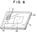
- Fig. 8 is a perspective view seeing through another structural example of the essential part of the thin IC card according to this invention.
- the thin IC card according to this invention is a so-called composite IC card.
- this thin IC card has both advantages and superiority of contact and non-contact type IC cards, and adopts a structure capable of easily fitting an only function section which relates to main information processing.
- this IC card has one element which is a plate type IC module in which a semiconductor chip having at least memory function and CPU function is sealed on its one side with a resin, and externally connecting terminals to be connected to the input/output terminals of the semiconductor chip are flatly led and exposed to a non-resin sealed or molded side.
- the plate type IC module is structured to be able to be optionally attached to or removed from a card-like support which includes therein a required circuit wiring, an antenna for sending and receiving a signal without contacting, and if necessary an oscillator for specifying a frequency and a power supply battery.
- the card-like support is provided with versatility, so that the plate type IC module can be removed and changed to easily meet various applications.
- Fig. 1 is a perspective view seeing through a rough structural embodiment of the thin IC card according to this invention.
- Fig. 2 is a sectional view taken along line A-A of Fig. 1.
- reference numeral 1 is a plate type IC module.
- the plate type IC module 1 includes a semiconductor chip (IC chip) having at least memory and CPU functions and having its one side sealed or molded with a resin, and flat type externally connecting terminals la which have their one end connected to the input/output terminals of the semiconductor chip and the other end led and exposed to a non-resin sealed or molded side.
- Reference numeral 2 is a card-like support which is configured such that the plate type IC module 1 can be fitted easily.
- the card-like support 2 includes therein a required circuit wiring, an antenna 2a for sending and receiving a signal without contacting and a power supply battery 2b, and has a fitting section for fitting the plate type IC module 1 with the side of its externally connecting terminals la exposed to be substantially flush with the surface of the card.
- the plate type IC module 1 is structured as shown in Fig. 3 which perspectively shows one side sealed or molded with a resin, Fig. 4 which perspectively shows the other side (reverse side) not sealed or molded with a resin, and Fig. 5 which shows a cross section taken along line B-B of Fig. 3.
- a CPU lb including a nonvolatile semiconductor memory is placed on the surface of a so-called through-hole resin type wiring board lc by a wire bonding ld.
- the through-hole wiring board lc has dimensions of, for example, approximately 14.0mm long, 13.0mm wide, and 0.3mm thick.
- the CPU 1b may include a static electricity resistant element for input/output and for preventing electrostatic breakdown, if necessary.
- flip chip bonding which directly applies the reverse side of the CPU lb to the surface of the wiring board 1c, may be used instead of the wire bonding 1d.
- the packaged thin plate type IC module 1 may have a structure in that its one side having the CPU 1b is not entirely sealed or molded with the resin layer 1e but partly coated or sealed to fill a space between the IC chip lb and the wiring board 1c as shown in the sectional view of Fig.
- the through-hole wiring board 1c whose one side is sealed, or the back side (non-resin sealed or molded side) of the plate type IC module 1 has the flat (flat type) terminals 1a which are led through the through holes.
- the flat terminals la have their surface plated with gold (Au) and, when they are used in a contact type, they functions as externally connecting terminals to electrically connect with the contacts of external equipment (read/writer).
- the card-like support 2 has dimensions (85.6mm long, 54.0mm wide, and 0.76mm thick) according to the standard of, for example, JEIDA, and is provided with a fitting section for fitting or mounting at least the plate type IC module 1 with the surface of the externally connecting terminals la of the plate type IC module 1 exposed to be flush with the surface of the card-like support 2.
- the card-like support 2 has the antenna 2a for sending and receiving a signal without contacting and the power supply battery 2b built in (internally disposed), embedded, fitted or mounted, and also has a wiring circuit, which electrically connects the aforementioned fitted or mounted respective parts to cause the required functions of the card to operate, built in or embedded.
- the wiring circuit is internally arranged in the card-like support 2 in the form of a single layer or multiple layers, and the antenna 2a for sending and receiving a signal without contacting is generally arranged internally in the circumferential area within the card-like support 2.
- the plate type IC module 1 when the plate type IC module 1 is fitted or mounted in the fitting section of the card-like support 2, the plate type IC module 1 can be electrically connected to the connection terminals of the internally arranged wiring circuit.
- the power supply battery 2b which is built in, embedded, fitted or mounted to the card-like support 2 may be a secondary battery, which can be externally charged through the externally connecting terminals la of the plate type IC module 1.
- the card-like wiring board which has the required circuit wiring and the antenna 2a for sending and receiving a signal without contacting therein, is formed.
- This card-like wiring board is produced by a conventional technology for producing printed wiring boards, such as photo-etching, lithography, and laminating technologies.
- the card-like support 2 is produced by disposing a structure to fit or build-in the plate type IC module 1 and the power supply battery 2b in prescribed areas of the formed card-like wiring board.
- the power supply battery 2b may be previously embedded in the previous process of forming the card-like wiring board.
- the plate type IC module 1 is fitted and arranged in the fitting section for the plate type IC module, which is formed in a prescribed area of the card-like support 2, with the surface of the externally connecting terminals 1a of the plate type IC module 1 exposed to be substantially flush with the surface of the card.
- the plate type IC module 1 is fitted to the card-like support 2, it is electrically connected to the connecting terminals which are previously arranged in the fitting section for the plate type IC module.
- the power supply battery 2b and the like are built in or arranged in prescribed areas in the card-like support 2 and electrically connected to the prescribed circuit wiring, thereby completing the assembling and the production of a desired thin film IC card.
- the wiring board body having the required circuit wiring may be formed previously, and several resin film layers may be applied to either side of the wiring board body.
- a structure to position and apply an insulating thin plate 3 having a thickness of about 0.3mm which has a window 3a to expose and fit the flat type externally connecting terminals la of the plate type IC module 1 and a recessed fitting section for the power supply battery 2b a card-like circuit board body 3' having a thickness of about 0.3mm which has open fitting sections for the IC module 1 and the power supply battery 2b and the built-in antenna 2a electrically connected to the circuit wiring, and an insulating thin plate 3'' having a thickness of about 0.16mm to one another into three layers.
- the above structure includes the power supply battery 2b
- the provision or attachment of the power supply battery 2b may be omitted.
- the antenna 2a for sending and receiving a signal without contacting which is provided or built in the card-like support 2
- an electric wave whose wavelength is changed is applied at timing different from the signal to generate electric power by electromagnetic induction.
- the required functions can be given to the non-contact type IC card even when the power supply battery 2b is omitted.
- Fig. 8 is a perspective view seeing through another rough structural embodiment of the thin IC card according to this invention, in which reference numeral 1 is a plate type IC module.
- This plate type IC module 1 includes a semiconductor chip (IC chip) having at least memory and CPU functions and having its one side sealed or molded with a resin, and flat type externally connecting terminals la which have their one end connected to the input/output terminals of the semiconductor chip and the other end led and exposed to a non-resin sealed or molded side.
- Reference numeral 2 is a card-like support which is configured such that the plate type IC module 1 can be attached or removed freely.
- the card-like support 2 includes therein a required circuit wiring (not shown), an antenna 2a for sending and receiving a signal without contacting, an oscillator 2c for specifying a frequency and a power supply battery 2b, and has a fitting section for fitting the plate type IC module 1 therein with the surface of the externally connecting terminals la exposed to be substantially flush with the surface of the card.
- the plate type IC module 1 has the same structure as in Embodiment 1. That is, it is structured as shown in Fig. 3 which perspectively shows one side sealed or molded with a resin, Fig. 4 which perspectively shows the other side (reverse side) not sealed or molded with a resin, and Fig. 5 which shows a cross section.
- a CPU 1b including a nonvolatile semiconductor memory is placed on the surface of so-called through-hole resin type wiring board 1c by a wire bonding 1d.
- the through-hole wiring board 1c has dimensions of, for example, approximately 14.0mm long, 13.0mm wide, and 0.30mm thick.
- the CPU 1b may include a static electricity resistant element for input/output and for preventing electrostatic breakdown, if necessary.
- the wiring board 1c on which the CPU 1b including a nonvolatile semiconductor memory is mounted has its one side sealed or molded with, for example, a transfer mold layer le to form the thin plate type IC module 1 which is packaged to have a total thickness of about 0.6mm.
- flip chip bonding which directly applies the reverse side of the CPU 1b to the surface of the wiring board 1c, may be used instead of the wire bonding 1d.
- the packaged thin plate type IC module 1 may have a structure that its one side having the IC chip 1b is not entirely sealed or molded with a resin but partly coated or sealed to fill a space between the IC chip lb and the wiring board 1c as shown in Fig. 6.
- the through-hole wiring board 1c whose one side is sealed, or the back side (non-resin sealed or molded side) of the plate type IC module 1 has the flat (flat type) terminals la, which are led through the through holes, arranged to form a package.
- the flat terminals la have their surface plated with gold (Au) and, when they are used in a contact type, they function as externally connecting terminals to electrically connect with the contacts of external equipment (read/writer).
- the card-like support 2 has dimensions (85.6mm long, 54.0mm wide, and 0.76mm thick) according to the standard of, for example, JEIDA, and is provided with a fitting section for fitting or mounting at least the plate type IC module 1 with the surface of the externally connecting terminals la of the plate type IC module 1 exposed to be flush with the surface of the card-like support 2.
- the card-like support 2 has the antenna 2a for sending and receiving a signal without contacting, the oscillator 2c for specifying a frequency and the power supply battery 2b built in, embedded, fitted or mounted, and also has a wiring circuit, which electrically connects the aforementioned fitted or mounted respective parts to cause the required functions of the card to operate, built in or embedded.
- the wiring circuit is internally arranged in the card-like support 2 in the form of a single layer or multiple layers, and the antenna 2a for sending and receiving a signal without contacting is generally arranged internally in the circumferential area within the card-like support 2.
- the externally connecting terminals of the plate type IC module 1 are electrically connected to the connection terminals of the internally arranged wiring circuit.
- the power supply battery 2b which is built in, embedded, fitted or mounted to the card-like support 2 may be a secondary battery which can be externally charged through the externally connecting terminals 1a of the plate type IC module 1.
- the card-like wiring board having the required circuit wiring and the antenna for sending and receiving a signal without contacting therein is formed.
- This card-like wiring board is produced by a conventional technology for producing printed wiring boards, such as photo-etching, lithography, and laminating technologies.
- the card-like support 2 is produced by disposing a structure to fit or build-in the plate type IC module 1, the oscillator 2c for specifying a frequency and the power supply battery 2b in prescribed areas of the formed card-like wiring board.
- the oscillator for specifying a frequency and the power supply battery 2b may be previously embedded in the previous process of forming the card-like wiring board.
- the plate type IC module 1 is fitted and arranged in the fitting section for the plate type IC module, which is formed in a prescribed area of the card-like support 2, with the surface of the externally connecting terminals 1a of the plate type IC module exposed to be substantially flush with the surface of the card.
- the plate type IC module 1 is electrically connected to the connecting terminals which are previously arranged in the fitting section for the plate type IC module, and connected to the circuit wiring of the card-like support 2.
- the oscillator 2c and the power supply battery 2b are built in or arranged in prescribed ares in the card-like support 2 and electrically connected to the prescribed circuit wiring, thereby completing the assembling and the production of a desired thin film IC card.
- this thin IC card has both functions of the contact and non-contact cards.
- the semiconductor device section having memory and CPU functions mainly contributing (relating) to the functions of the card, is formed into a flat module piece, and this flat module piece can be easily attached to or removed from the card-like support.
- this thin film IC card having multiple functions can be used for example as a bank card, a wireless card which saves a certain amount of money withdrawn form the bank and pays various charges like a prepaid card, or used as a commuter pass and an ID card by devising software.
Landscapes
- Engineering & Computer Science (AREA)
- Microelectronics & Electronic Packaging (AREA)
- Computer Hardware Design (AREA)
- Physics & Mathematics (AREA)
- General Physics & Mathematics (AREA)
- Theoretical Computer Science (AREA)
- Credit Cards Or The Like (AREA)
Applications Claiming Priority (6)
| Application Number | Priority Date | Filing Date | Title |
|---|---|---|---|
| JP21750493 | 1993-09-01 | ||
| JP217504/93 | 1993-09-01 | ||
| JP21750493 | 1993-09-01 | ||
| JP31863293 | 1993-12-17 | ||
| JP5318632A JPH07117385A (ja) | 1993-09-01 | 1993-12-17 | 薄型icカードおよび薄型icカードの製造方法 |
| JP318632/93 | 1993-12-17 |
Publications (3)
| Publication Number | Publication Date |
|---|---|
| EP0646895A2 true EP0646895A2 (fr) | 1995-04-05 |
| EP0646895A3 EP0646895A3 (fr) | 1995-06-28 |
| EP0646895B1 EP0646895B1 (fr) | 2000-01-19 |
Family
ID=26522051
Family Applications (1)
| Application Number | Title | Priority Date | Filing Date |
|---|---|---|---|
| EP94304992A Expired - Lifetime EP0646895B1 (fr) | 1993-09-01 | 1994-07-06 | Carte à puce mince et méthode de sa fabrication |
Country Status (5)
| Country | Link |
|---|---|
| US (1) | US5612532A (fr) |
| EP (1) | EP0646895B1 (fr) |
| JP (1) | JPH07117385A (fr) |
| KR (1) | KR0131271B1 (fr) |
| DE (1) | DE69425592T2 (fr) |
Cited By (9)
| Publication number | Priority date | Publication date | Assignee | Title |
|---|---|---|---|---|
| WO1997005570A1 (fr) * | 1995-08-01 | 1997-02-13 | Austria Card Plastikkarten Und Ausweissysteme Gesellschaft Mbh | Support de donnees sous forme de carte pour applications sans contact, comportant un composant et un systeme de transmission pour applications sans contact, procede permettant de produire un support de donnees sous forme de carte de ce type et module approprie |
| WO1997005569A1 (fr) * | 1995-08-01 | 1997-02-13 | Austria Card Plastikkarten Und Ausweissysteme Gesellschaft Mbh | Support de donnees comportant un module pourvu d'un composant et d'une bobine, et procede de fabrication dudit support de donnees |
| WO1997005571A1 (fr) * | 1995-08-01 | 1997-02-13 | Austria Card Plastikkarten Und Ausweissysteme Gesellschaft Mbh | Support de donnees muni d'un module comportant un composant et d'une bobine, procede de production d'un support de donnees de ce type et module approprie |
| WO1997011437A2 (fr) * | 1995-09-18 | 1997-03-27 | David Finn | Module carte de ci pour la fabrication d'une carte de ci et procede de fabrication d'une carte de ci |
| DE19800341A1 (de) * | 1997-11-12 | 1999-05-20 | Meinen Ziegel & Co Gmbh | IC-Karte, insbesondere für ein schlüsselloses Zugangssystem |
| EP1035526A2 (fr) * | 1999-03-05 | 2000-09-13 | Sony Corporation | Système de monnaie électronique, dispositif de terminal de monnaie électronique et carte d'information |
| WO2003071475A2 (fr) * | 2002-02-19 | 2003-08-28 | Orga Kartensysteme Gmbh | Carte a puce |
| DE19612718B4 (de) * | 1996-03-29 | 2006-06-29 | Ods Landis & Gyr Gmbh & Co. Kg | Chipkarte mit Batterie sowie Verfahren zur Montage einer Chipmodul/Batterie-Einheit |
| FR3089659A1 (fr) * | 2018-12-07 | 2020-06-12 | Smart Packaging Solutions | Carte à puce en métal à double interface de communication |
Families Citing this family (56)
| Publication number | Priority date | Publication date | Assignee | Title |
|---|---|---|---|---|
| DE4443980C2 (de) * | 1994-12-11 | 1997-07-17 | Angewandte Digital Elektronik | Verfahren zur Herstellung von Chipkarten und Chipkarte hergestellt nach diesem Verfahren |
| DE19512191C2 (de) * | 1995-03-31 | 2000-03-09 | Siemens Ag | Kartenförmiger Datenträger und Leadframe zur Verwendung in einem solchen Datenträger |
| CA2192076C (fr) * | 1995-04-13 | 2000-01-18 | Masao Gogami | Carte et module de circuit integre |
| US5817207A (en) | 1995-10-17 | 1998-10-06 | Leighton; Keith R. | Radio frequency identification card and hot lamination process for the manufacture of radio frequency identification cards |
| DE19654902C2 (de) * | 1996-03-15 | 2000-02-03 | David Finn | Chipkarte |
| KR100209259B1 (ko) * | 1996-04-25 | 1999-07-15 | 이해규 | Ic 카드 및 그 제조방법 |
| JPH09315061A (ja) * | 1996-06-03 | 1997-12-09 | Minolta Co Ltd | Icカードおよびicカード装着装置 |
| JPH09327990A (ja) * | 1996-06-11 | 1997-12-22 | Toshiba Corp | カード型記憶装置 |
| JP2001505329A (ja) * | 1996-08-05 | 2001-04-17 | ジェムプリュス エス.セー.アー. | メモリカード実現方法の改良とそれによって得られるカード |
| DE19632813C2 (de) * | 1996-08-14 | 2000-11-02 | Siemens Ag | Verfahren zur Herstellung eines Chipkarten-Moduls, unter Verwendung dieses Verfahrens hergestellter Chipkarten-Modul und diesen Chipkarten-Modul enthaltende Kombi-Chipkarte |
| US6011698A (en) * | 1996-11-12 | 2000-01-04 | Delco Electronics Corp. | Circuit protection from radio frequency energy |
| NZ336338A (en) * | 1996-11-20 | 2000-02-28 | Tecsec Inc | Cryptographic medium containing a plastic base with metallic slivers embedded within, processing means and storage means |
| DE19703990A1 (de) * | 1997-02-03 | 1998-08-06 | Giesecke & Devrient Gmbh | Modular aufgebauter, elektronischer Datenträger |
| FR2760113B1 (fr) * | 1997-02-24 | 1999-06-04 | Gemplus Card Int | Procede de fabrication de carte sans contact a antenne bobinee |
| US6049463A (en) * | 1997-07-25 | 2000-04-11 | Motorola, Inc. | Microelectronic assembly including an antenna element embedded within a polymeric card, and method for forming same |
| US6024285A (en) * | 1997-08-19 | 2000-02-15 | Micron Technology, Inc. | Wireless communication devices and methods of forming wireless communication devices |
| US6651891B1 (en) * | 1997-11-04 | 2003-11-25 | Elke Zakel | Method for producing contactless chip cards and corresponding contactless chip card |
| DE69933963T2 (de) * | 1998-03-24 | 2007-09-20 | Kabushiki Kaisha Toshiba | IC Karte mit kontaktbehafteten und kontaktlosen Schnittstellen |
| US6040622A (en) * | 1998-06-11 | 2000-03-21 | Sandisk Corporation | Semiconductor package using terminals formed on a conductive layer of a circuit board |
| US6525410B1 (en) * | 1998-07-24 | 2003-02-25 | Texas Instruments Incorporated | Integrated circuit wireless tagging |
| US6680817B1 (en) * | 1998-09-21 | 2004-01-20 | Sony Corporation | Recording medium device containing recording medium and recording/reproducing device |
| FR2784210B1 (fr) * | 1998-10-02 | 2001-09-14 | Gemplus Card Int | Carte a puce sans contact comportant des moyens d'inhibition |
| FR2785072B1 (fr) * | 1998-10-23 | 2001-01-19 | St Microelectronics Sa | Circuit electronique autocollant |
| FR2788646B1 (fr) * | 1999-01-19 | 2007-02-09 | Bull Cp8 | Carte a puce munie d'une antenne en boucle, et micromodule associe |
| JP3335938B2 (ja) * | 1999-03-01 | 2002-10-21 | 新光電気工業株式会社 | Icカード用アンテナフレーム及びicカードの製造方法 |
| AU4128899A (en) * | 1999-06-18 | 2001-01-09 | Swisscom Mobile Ag | Interchangeable battery pack for a mobile telephone |
| US6634561B1 (en) * | 1999-06-24 | 2003-10-21 | Sandisk Corporation | Memory card electrical contact structure |
| US6368901B2 (en) | 1999-07-15 | 2002-04-09 | Texas Instruments Incorporated | Integrated circuit wireless tagging |
| JP4299414B2 (ja) * | 1999-10-12 | 2009-07-22 | 富士通マイクロエレクトロニクス株式会社 | コンビネーションカード、icカード用モジュール及びコンビネーションカードの製造方法 |
| JP2001167242A (ja) * | 1999-12-10 | 2001-06-22 | Sony Corp | エンボス加工可能なicカード、その製造方法及びその情報読取確認システム |
| US6433285B2 (en) * | 2000-03-30 | 2002-08-13 | Matsushita Electronics Corporation | Printed wiring board, IC card module using the same, and method for producing IC card module |
| KR100727904B1 (ko) * | 2000-06-09 | 2007-06-13 | 삼성전자주식회사 | 칩 인베디드 트레이딩 카드, 이에 적합한 기록/재생 장치,그리고 이에 적합한 커뮤니케이션 구현 방법 |
| US6945461B1 (en) * | 2001-03-30 | 2005-09-20 | 3Com Corporation | Compact multifunction card for electronic devices |
| CN100435170C (zh) | 2001-04-02 | 2008-11-19 | 株式会社日立制作所 | 存储卡 |
| JP2002342731A (ja) * | 2001-05-16 | 2002-11-29 | Matsushita Electric Ind Co Ltd | 複合icカード |
| US20040212017A1 (en) * | 2001-08-07 | 2004-10-28 | Hirotaka Mizuno | Semiconductor device and ic card |
| US7177601B1 (en) * | 2001-11-02 | 2007-02-13 | Raytheon Company | Method and apparatus for transceiving data using a bimodal power data link transceiver device |
| JP2003288573A (ja) * | 2002-03-27 | 2003-10-10 | Seiko Epson Corp | Icカード及びその製造方法 |
| KR100910769B1 (ko) * | 2002-06-11 | 2009-08-04 | 삼성테크윈 주식회사 | Ic 카드 및, 그것의 제조 방법 |
| JP4141857B2 (ja) * | 2003-02-18 | 2008-08-27 | 日立マクセル株式会社 | 半導体装置 |
| JP4318967B2 (ja) * | 2003-06-16 | 2009-08-26 | Tdk株式会社 | Icカード |
| DE10343734A1 (de) * | 2003-09-22 | 2005-04-21 | Austria Card | Datenträgerkarte mit aufladbarer Batterie |
| US7177159B2 (en) * | 2004-05-03 | 2007-02-13 | 3 View Technology Co., Ltd. | Packaging structure of electronic card |
| US7444735B2 (en) * | 2004-06-15 | 2008-11-04 | Chartered Semiconductor Manufacturing Ltd. | Process for manufacturing an integrated circuit system |
| JPWO2007034764A1 (ja) * | 2005-09-26 | 2009-03-26 | パナソニック株式会社 | 非接触型情報記憶媒体とその製造方法 |
| JP2007183919A (ja) * | 2005-12-05 | 2007-07-19 | Nec Corp | Rfidタグ |
| JP5135780B2 (ja) * | 2005-12-05 | 2013-02-06 | 日本電気株式会社 | 電子デバイス |
| DE102009014343A1 (de) * | 2009-03-21 | 2010-09-23 | Deutsche Telekom Ag | Verfahren zum Herstellen einer eine kontaktlose und eine kontaktbehaftete Schnittstelle aufweisenden Chipkarte |
| US8649820B2 (en) | 2011-11-07 | 2014-02-11 | Blackberry Limited | Universal integrated circuit card apparatus and related methods |
| US8936199B2 (en) | 2012-04-13 | 2015-01-20 | Blackberry Limited | UICC apparatus and related methods |
| USD703208S1 (en) | 2012-04-13 | 2014-04-22 | Blackberry Limited | UICC apparatus |
| USD701864S1 (en) * | 2012-04-23 | 2014-04-01 | Blackberry Limited | UICC apparatus |
| US20140312123A1 (en) * | 2012-09-28 | 2014-10-23 | Smart Approach Co., Ltd. | Radio Frequency Identification Module |
| EP2933759A1 (fr) * | 2014-04-18 | 2015-10-21 | Gemalto SA | Procédé de fabrication d'un dispositif à circuit électronique/électrique |
| CN104166870B (zh) * | 2014-07-01 | 2018-04-27 | 珠海市金邦达保密卡有限公司 | 双界面金属智能芯片卡及其制造方法 |
| CN104166869A (zh) * | 2014-07-07 | 2014-11-26 | 珠海市金邦达保密卡有限公司 | 无源led闪光交易卡、制备方法及交易显示的方法 |
Citations (6)
| Publication number | Priority date | Publication date | Assignee | Title |
|---|---|---|---|---|
| EP0231384A1 (fr) * | 1985-07-17 | 1987-08-12 | Ibiden Co, Ltd. | Procédé de fabrication d'une plaquette à câblage imprimé pour cartes à circuits intégrés |
| JPH01185783A (ja) * | 1988-01-20 | 1989-07-25 | Mitsubishi Electric Corp | Icカード識別方式 |
| FR2647572A1 (fr) * | 1989-05-23 | 1990-11-30 | Mitsubishi Electric Corp | Carte a circuits integres et procede de fabrication de celle-ci |
| DE4105869A1 (de) * | 1991-02-25 | 1992-08-27 | Edgar Schneider | Ic-karte und verfahren zu ihrer herstellung |
| DE4218923A1 (de) * | 1992-06-10 | 1992-10-22 | Haiss Ulrich | Wertkarte mit elektronik-wert-chip |
| DE4243654A1 (en) * | 1991-12-26 | 1993-07-01 | Mitsubishi Electric Corp | Thin integrated circuit card with integral battery - contains circuit board with battery aperture in resin with aperture, connector holding battery in aperture |
Family Cites Families (7)
| Publication number | Priority date | Publication date | Assignee | Title |
|---|---|---|---|---|
| DE3935364C1 (fr) * | 1989-10-24 | 1990-08-23 | Angewandte Digital Elektronik Gmbh, 2051 Brunstorf, De | |
| DE4007221A1 (de) * | 1990-03-07 | 1991-09-12 | Gao Ges Automation Org | Pruefkopf fuer kontaktflaechen von wertkarten mit eingelagertem halbleiterchip |
| US5049728A (en) * | 1990-04-04 | 1991-09-17 | Rovin George H | IC card system with removable IC modules |
| JPH0416831A (ja) * | 1990-05-11 | 1992-01-21 | Nec Corp | 非線形光学素子の作製方法 |
| JPH04168094A (ja) * | 1990-10-31 | 1992-06-16 | Mitsubishi Electric Corp | 携帯形半導体記憶装置 |
| EP0492482B1 (fr) * | 1990-12-28 | 1996-10-23 | Mitsubishi Denki Kabushiki Kaisha | Carte à puce du type sans contacts |
| JP2896031B2 (ja) * | 1992-12-28 | 1999-05-31 | 三菱電機株式会社 | 非接触icカードの端末機および非接触icカードシステム |
-
1993
- 1993-12-17 JP JP5318632A patent/JPH07117385A/ja active Pending
-
1994
- 1994-07-06 DE DE69425592T patent/DE69425592T2/de not_active Expired - Lifetime
- 1994-07-06 EP EP94304992A patent/EP0646895B1/fr not_active Expired - Lifetime
- 1994-08-31 KR KR94021754A patent/KR0131271B1/ko not_active IP Right Cessation
-
1995
- 1995-11-09 US US08/554,927 patent/US5612532A/en not_active Expired - Lifetime
Patent Citations (6)
| Publication number | Priority date | Publication date | Assignee | Title |
|---|---|---|---|---|
| EP0231384A1 (fr) * | 1985-07-17 | 1987-08-12 | Ibiden Co, Ltd. | Procédé de fabrication d'une plaquette à câblage imprimé pour cartes à circuits intégrés |
| JPH01185783A (ja) * | 1988-01-20 | 1989-07-25 | Mitsubishi Electric Corp | Icカード識別方式 |
| FR2647572A1 (fr) * | 1989-05-23 | 1990-11-30 | Mitsubishi Electric Corp | Carte a circuits integres et procede de fabrication de celle-ci |
| DE4105869A1 (de) * | 1991-02-25 | 1992-08-27 | Edgar Schneider | Ic-karte und verfahren zu ihrer herstellung |
| DE4243654A1 (en) * | 1991-12-26 | 1993-07-01 | Mitsubishi Electric Corp | Thin integrated circuit card with integral battery - contains circuit board with battery aperture in resin with aperture, connector holding battery in aperture |
| DE4218923A1 (de) * | 1992-06-10 | 1992-10-22 | Haiss Ulrich | Wertkarte mit elektronik-wert-chip |
Non-Patent Citations (1)
| Title |
|---|
| PATENT ABSTRACTS OF JAPAN vol. 013 no. 475 (P-950) ,27 October 1989 & JP-A-01 185783 (MITSUBISHI ELECTRIC CORP) 25 July 1989, * |
Cited By (19)
| Publication number | Priority date | Publication date | Assignee | Title |
|---|---|---|---|---|
| WO1997005569A1 (fr) * | 1995-08-01 | 1997-02-13 | Austria Card Plastikkarten Und Ausweissysteme Gesellschaft Mbh | Support de donnees comportant un module pourvu d'un composant et d'une bobine, et procede de fabrication dudit support de donnees |
| WO1997005571A1 (fr) * | 1995-08-01 | 1997-02-13 | Austria Card Plastikkarten Und Ausweissysteme Gesellschaft Mbh | Support de donnees muni d'un module comportant un composant et d'une bobine, procede de production d'un support de donnees de ce type et module approprie |
| WO1997005570A1 (fr) * | 1995-08-01 | 1997-02-13 | Austria Card Plastikkarten Und Ausweissysteme Gesellschaft Mbh | Support de donnees sous forme de carte pour applications sans contact, comportant un composant et un systeme de transmission pour applications sans contact, procede permettant de produire un support de donnees sous forme de carte de ce type et module approprie |
| US6310778B1 (en) | 1995-09-18 | 2001-10-30 | David Finn | IC board module for producing an IC board and process for producing an IC board |
| WO1997011437A2 (fr) * | 1995-09-18 | 1997-03-27 | David Finn | Module carte de ci pour la fabrication d'une carte de ci et procede de fabrication d'une carte de ci |
| WO1997011437A3 (fr) * | 1995-09-18 | 1997-04-17 | David Finn | Module carte de ci pour la fabrication d'une carte de ci et procede de fabrication d'une carte de ci |
| DE19612718B4 (de) * | 1996-03-29 | 2006-06-29 | Ods Landis & Gyr Gmbh & Co. Kg | Chipkarte mit Batterie sowie Verfahren zur Montage einer Chipmodul/Batterie-Einheit |
| DE19800341C2 (de) * | 1997-11-12 | 2002-02-14 | Meinen Ziegel & Co Gmbh | IC-Karte, insbesondere für ein schlüsselloses Zugangssystem |
| DE19800341A1 (de) * | 1997-11-12 | 1999-05-20 | Meinen Ziegel & Co Gmbh | IC-Karte, insbesondere für ein schlüsselloses Zugangssystem |
| EP1035526A2 (fr) * | 1999-03-05 | 2000-09-13 | Sony Corporation | Système de monnaie électronique, dispositif de terminal de monnaie électronique et carte d'information |
| EP1035526A3 (fr) * | 1999-03-05 | 2003-05-28 | Sony Corporation | Système de monnaie électronique, dispositif de terminal de monnaie électronique et carte d'information |
| US7366699B1 (en) | 1999-03-05 | 2008-04-29 | Sony Corporation | Electronic money system, electronic money terminal device, and information card |
| WO2003071475A2 (fr) * | 2002-02-19 | 2003-08-28 | Orga Kartensysteme Gmbh | Carte a puce |
| DE10207000A1 (de) * | 2002-02-19 | 2003-09-04 | Orga Kartensysteme Gmbh | Chipkarte |
| DE10207000C2 (de) * | 2002-02-19 | 2003-12-11 | Orga Kartensysteme Gmbh | Chipkarte |
| WO2003071475A3 (fr) * | 2002-02-19 | 2004-04-01 | Orga Kartensysteme Gmbh | Carte a puce |
| FR3089659A1 (fr) * | 2018-12-07 | 2020-06-12 | Smart Packaging Solutions | Carte à puce en métal à double interface de communication |
| WO2020115375A3 (fr) * | 2018-12-07 | 2020-08-06 | Smart Packaging Solutions | Carte à puce en métal à double interface de communication |
| US11630978B2 (en) | 2018-12-07 | 2023-04-18 | Smart Packaging Solutions | Metal chip card with dual communication interface |
Also Published As
| Publication number | Publication date |
|---|---|
| JPH07117385A (ja) | 1995-05-09 |
| KR0131271B1 (en) | 1998-04-24 |
| EP0646895A3 (fr) | 1995-06-28 |
| DE69425592T2 (de) | 2000-12-14 |
| EP0646895B1 (fr) | 2000-01-19 |
| US5612532A (en) | 1997-03-18 |
| DE69425592D1 (de) | 2000-09-21 |
Similar Documents
| Publication | Publication Date | Title |
|---|---|---|
| EP0646895B1 (fr) | Carte à puce mince et méthode de sa fabrication | |
| JP3305843B2 (ja) | 半導体装置 | |
| US5598032A (en) | Hybrid chip card capable of both contact and contact-free operation and having antenna contacts situated in a cavity for an electronic module | |
| EP1535240B1 (fr) | Module d'identite d'abonne (sim), module a circuit integre et carte a circuit integre | |
| US5671525A (en) | Method of manufacturing a hybrid chip card | |
| JP2000311226A (ja) | 無線icカード及びその製造方法並びに無線icカード読取り書込みシステム | |
| US7577406B2 (en) | Wireless transceiver for automotive vehicle | |
| JP3571057B2 (ja) | チップカード及びチップカードの製造方法 | |
| EP1887495A2 (fr) | Étiquette RFID et procédé de lecture correspondant | |
| KR20000012026A (ko) | 무선ic카드와그제조방법및데이터판독기록장치및무선태그와그제조방법 | |
| JP2002342731A (ja) | 複合icカード | |
| JPH11149536A (ja) | 複合icカード | |
| WO2018158644A1 (fr) | Carte à puce et procédé de fabrication d'une carte à puce | |
| JPH11509024A (ja) | カードまたはラベル用の非接触電子モジュール | |
| JP2001043340A (ja) | 複合icカード | |
| CN114764606A (zh) | 用于直接连接或电感耦合技术的卡嵌体 | |
| KR20080113056A (ko) | Ic 모듈, ic 인레트 및 ic 실장체 | |
| CN107111779B (zh) | 包括互连区的单面电子模块的制造方法 | |
| KR19990076679A (ko) | 비접촉식 기술에서 사용하기 위한 칩카드의 제조방법 | |
| JPH11328341A (ja) | 複合icカード | |
| JP2001175828A (ja) | 非接触icカード | |
| JP2001209772A (ja) | 非接触伝達機構付icカード | |
| JPH1134558A (ja) | Icカードおよびicカード用のicモジュール | |
| JPH11213119A (ja) | 複合型icカード | |
| JP2004287472A (ja) | Icチップモジュール並びにicカード |
Legal Events
| Date | Code | Title | Description |
|---|---|---|---|
| PUAI | Public reference made under article 153(3) epc to a published international application that has entered the european phase |
Free format text: ORIGINAL CODE: 0009012 |
|
| 17P | Request for examination filed |
Effective date: 19940727 |
|
| AK | Designated contracting states |
Kind code of ref document: A2 Designated state(s): DE FR GB |
|
| PUAL | Search report despatched |
Free format text: ORIGINAL CODE: 0009013 |
|
| AK | Designated contracting states |
Kind code of ref document: A3 Designated state(s): DE FR GB |
|
| 17Q | First examination report despatched |
Effective date: 19971229 |
|
| GRAG | Despatch of communication of intention to grant |
Free format text: ORIGINAL CODE: EPIDOS AGRA |
|
| GRAG | Despatch of communication of intention to grant |
Free format text: ORIGINAL CODE: EPIDOS AGRA |
|
| GRAH | Despatch of communication of intention to grant a patent |
Free format text: ORIGINAL CODE: EPIDOS IGRA |
|
| GRAH | Despatch of communication of intention to grant a patent |
Free format text: ORIGINAL CODE: EPIDOS IGRA |
|
| GRAA | (expected) grant |
Free format text: ORIGINAL CODE: 0009210 |
|
| AK | Designated contracting states |
Kind code of ref document: B1 Designated state(s): DE FR GB |
|
| ET | Fr: translation filed | ||
| REF | Corresponds to: |
Ref document number: 69425592 Country of ref document: DE Date of ref document: 20000921 |
|
| PLBE | No opposition filed within time limit |
Free format text: ORIGINAL CODE: 0009261 |
|
| STAA | Information on the status of an ep patent application or granted ep patent |
Free format text: STATUS: NO OPPOSITION FILED WITHIN TIME LIMIT |
|
| 26N | No opposition filed | ||
| REG | Reference to a national code |
Ref country code: GB Ref legal event code: IF02 |
|
| PGFP | Annual fee paid to national office [announced via postgrant information from national office to epo] |
Ref country code: FR Payment date: 20110727 Year of fee payment: 18 |
|
| PGFP | Annual fee paid to national office [announced via postgrant information from national office to epo] |
Ref country code: DE Payment date: 20110629 Year of fee payment: 18 Ref country code: GB Payment date: 20110706 Year of fee payment: 18 |
|
| GBPC | Gb: european patent ceased through non-payment of renewal fee |
Effective date: 20120706 |
|
| REG | Reference to a national code |
Ref country code: FR Ref legal event code: ST Effective date: 20130329 |
|
| PG25 | Lapsed in a contracting state [announced via postgrant information from national office to epo] |
Ref country code: GB Free format text: LAPSE BECAUSE OF NON-PAYMENT OF DUE FEES Effective date: 20120706 Ref country code: DE Free format text: LAPSE BECAUSE OF NON-PAYMENT OF DUE FEES Effective date: 20130201 Ref country code: FR Free format text: LAPSE BECAUSE OF NON-PAYMENT OF DUE FEES Effective date: 20120731 |
|
| REG | Reference to a national code |
Ref country code: DE Ref legal event code: R119 Ref document number: 69425592 Country of ref document: DE Effective date: 20130201 |